IMPROVEMENT OF OPTICAL CHARACTERISTICS OF COMPONENTS OF OPTOELECTRONIC
DEVICES IN THE HARSH CONDITIONS OF THEIR FUNCTIONING BY USING ELECTRON BEAM
TECHNOLOGY
УЛУЧШЕНИЕ ОПТИЧЕСКИХ
ХАРАКТЕРИСТИК ЭЛЕМЕНТОВ ОПТИКО
-
ЭЛЕКТРОННЫХ
ПРИБОРОВ В ЖЕСТКИХ УСЛОВИЯХ ИХ ФУНКЦИОНИРОВАНИЯ ПРИ ПОМОЩИ ЭЛЕКТРОННО
-ЛУЧЕВОЙ ТЕХНОЛОГИИ
PhD, Associate Professor Yacenko I. V1. , d. Eng. Sc., Professor Antoniuk V. C.2, d. Eng. Sc., Associate Professor Kyrychenko O. V.3 , d. Eng. Sc. Gordienko V. I. 4 , d. Eng. Sc. , Professor Vashchenko V. A 1
Cherkasy State technological university1 , Ukraine, National Technical University of Ukraine " Kiev Polytechnic Institute name of Igor Sikorsky"2, Cherkassy Institute of Fire Safety named after Heroes of Chornobyl3,
Ukraine, State Enterprise scientific-production complex “Photoprylad”4, Ukraine Е-mail: [email protected]
Summary: The optimal parameters of the ranges of the electron beam are found (heat density, velocity, displacement), within which there is improvement of the physical and mechanical properties of surface layers of optical elements: there is no formation of negative defects on their surfaces which become atomically smooth (residual microscopic ridges do not exceed 0.5… 1.5 nm); the microhardness of the surface increases, hardened layers are formed with compressive stresses. This leads to the reduction of the light scattering coefficient of surface layers of elements and increase of their coefficient of infrared radiation transmittance and, ultimately, to the improvement of metrological characteristics and reliability of devices under intensive external thermal action.
KEYWORDS: OPTOELECTRONIC DEVICES, OPTICAL GLASS, OPTICAL CERAMICS, ELECTRON BEAM, OPTICAL CHARACTERISTICS
1.
Introduction
The areas of application of modern opto-electronic devices, which constantly expand, acutely raise the problem of enhancing of their effective functioning under harsh conditions.
Optical elements of devices under these conditions are subjected to intense external influences (elevation of heating temperature, external pressures, percussive thermal actions under conditions of supersonic airflow and axial rotation of the optical elements (hemispherical fairings, flat visibility windows etc.)).
These external influences lead to the formation on the surface of optical elements and their surface layers of cracks, chips, undulating surfaces, which violate the flatness of the elements, and other negative defects. Thereat physical and mechanical properties of the surface layers of optical elements deteriorate, and, ultimately, their optical characteristics that affect the metrological characteristics and reliability of optoelectronic devices when they are functioning under the conditions of external thermal actions [1-4].
Existing methods of improving optical characteristics of optical-electronic devices (laser range finders of sighting complexes, laser medical devices, IR-homing and tracking devices, space and aerospace grade mirrors etc.) do not always provide their normative values, especially under harsh operating conditions.
New possibilities of improvement of optical characteristics of devices are opened due to the targeted change of the physico-mechanical and thermal properties of the surface layer of optical elements by modifying it. One of the effective methods of surface treatment of optical materials is the moving electron beam, which allows to modify the surface layers of optical elements by changing its physico-mechanical properties, which influence the optical characteristics of elements, metrological characteristics and reliability of devices [5 – 13].
Phenomena connected with the influence of technological parameters of forming and physico-mechanical characteristics of the surface layer of the optical elements of the devices are not fully studied and not systematized.
This determinates the relevance of development property management methods of working surfaces of optical elements of devices by using electron-beam finishing methods of optical elements that improve the physical and mechanical properties of surface layers, increasing their optical characteristics,
and resistance to external thermal and mechanical influences, that allows to increase accuracy, extend measuring ranges and improve the reliability of the functioning of the devices under intensive external thermal actions.
Therefore, the aim of this work is to improve the optical characteristics of the elements of optoelectronic devices by their finish electron beam processing.
2.
Characteristics of optical elements and
research methods
For experimental studies modern methods of physico-chemical analysis were used [5, 14, 15]: methods of scanning electron microscopy (SEM) and transemission electron microscopy (TEM) to study surface structure and surface layers of optical elements, as well as determine the thickness of melted layers ; methods of atomic force microscopy (AFM) and micro identification by Vickers for the measurement of the residual voids on the surface of optical elements, as well as its microhardness; shooting techniques in x-rays of diffractometers DRONE 2.0 and DRONE 3.0 for measurem ents of thermal stresses in the surface layers of optical elements; methods with using spectrophotometers of close (λ = 0,76…2,5 µm ) and far (λ = 2,5…25 µm) of IR ranges for the measurement of transmittance factor of IR waves of optical elements; contact methods (chromel-alumel thermocouples, temperature measurement range up to 1600 K) and contactless methods (photoresistors, temperature measurement range up to 1600 K) to measure the surface temperature of the optical elements.
For finish electron beam processing of surface layers of optical elements aiming to improve their physical and mechanical properties advanced installation was used (fig. 1) in the part of developed tooling for automated measurement and control of temperature of the surface, as well as sensing the electron beam, which is protected by patents (patent of Ukraine № 57551, patent of Ukraine № 91523) [5, 6].
The following empirical dependencies on density of thermal influence in its center from managed parameters of electron beam installation (relative accuracy of 5…8%) were found out in the result of the research on sensing the electron beam by the known method of rotary probe [5]:
( )
( )
( )
( )
[
bI ,l k I ,l]
erfB
V I l
, I k x F
л л
у л л
n
0 0
⋅ ⋅
⋅ ⋅
=
π , (1)
( )
I ,lk0 л = 1,237∙107-6,587∙105l-3,725∙104Iл+1,518∙102I lл , (2)
( )
( )
I ,l k, l , I b
л л
0
75 1
, (3)
where Fn – the density of the thermal influence in the center of the
electron beam, Wt/m2; k0, 2b – concentration ratio (severity of the
thermal pulse) and the thickness of the electron beam, m; Iл – beam
current, mA; Vу – external voltage, qt; l – the distance from the processed surface of the optical element, m. Found out, that for working ranges of changing of stated parameters of installation (Iл = 50…300 mА, Vу = 6...8 qt, l = 0,04...0,08 m) the following variation ranges of energy caracteristics of electron beam are realized: k0 = (0,5…5)⋅107 m-2; 2b = (0,5…1,5)⋅10-3 m; Fn =
106…109 Wt/m2. Herein beam travel speed changed within V = 0…0,1 m/s.
Вакуумная камера Пушка Пирса
Кварцевые нагреватели
Зажимное устройство с объектом обработки
Механизм перемещения
Электродвигатель
Насос Вакуумныйпост Блок электро-привода Питание кварцевой печи
Система зондов Модуль формирования ускоряющего напряжения Модуль формирования тока разогрева катода
Модуль питания электронной пушки
C
A
N
-ш
ин
а Система автоматизированного управления
Вакуумная система
a) b)
Fig. 1. Appearance (a) and schema (b) installations for the finishing electron-beam processing of optical elements, which improves the physical-mechanical properties of their surface layers: 1 – vacuum gauge magnetic locking VMB-8 (ВМБ-8) ; 2 – gauge ionized-thermocouple VIT-3(ВИТ-3); 3 – vacuum chamber; 4-electric mechanism of transfer mechanism of optical elements; 5 – PC control; 6 – modules of temperature measurement in the treatment area and sensing electronic flow; 7 – thermal management system of optical elements based on device RIF-101 (РИФ-101); 8 – central unit of automatic control system; 9 – power supply and control system of electronic gun of Pierce; 10 – electric motor control.
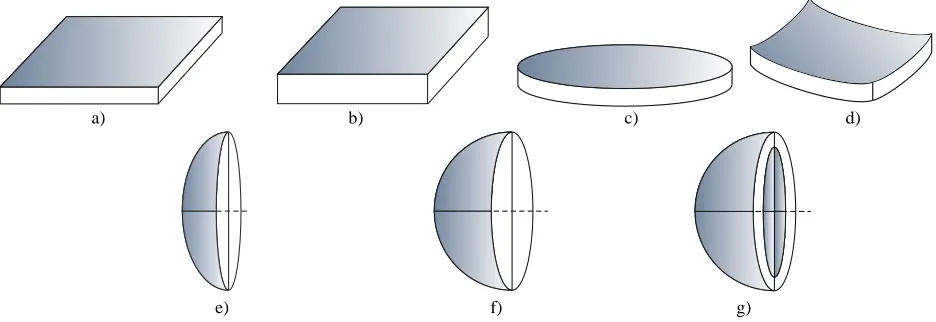
For pilot studies they used samples of optical elements of optoelectronic devices [14-18]: plane-parallel plates, rectangular,
cylindrical and spherical elements elements, dual curvature elements from optical glass (К8, К108, К208, BK10 (БК10), TF110 (ТФ110)) and optical ceramics (KO1, KO2, KO3, KO5, KO12) (fig. 2).
a) b) c) d)
e) f) g)
Fig. 2. General view of the optical elements of devices: flat-parallel plates (a), rectangular elements (b), disks (c), plates of double curvature (d) (substrates, light scattering screens in micro optics, integrated and fiber optics; elements of aerospace mirrors) and spherical elements (e) – (g) (lenses, hemispherical fairings).
3. Results and discussions
Optimal variation ranges of the parameters of the electron beam are defined: heat density Fn= 7∙106...8∙108 Wt/m2 and velocity V = 5∙10-3... 5∙10-2 m/s, within which there is improvement of parameters of surface layers of optical elements.
Electron-microscopic studies of surfaces of optical glass elements showed that after machining the most characteristic is the presence of microflaws – cracks up to 0.1 ... 0.7 µm deep, scratches with length up to 2 ... 5 µm, bubbles in size 10-3...10-2 µm.
After the electron beam processing the bubble sizes (diameters) on the surface of elements reduction in 2 ... 4 times, while other wavinesses less than 1 ... 2 microns are not observed,
6
7
5
8
3
10
4
2
1
that means in electron beam processing the surfaces of elements as would be "cleaned up", tiny defects are eliminated.
In this case, when you increase the heat density Fп from 5∙106 Wt/m2 to 7∙107 Wt/m2 the area of specified defects decreases in 1,8...2,7 times.
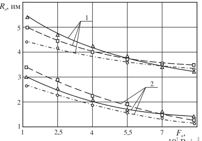
Study of the skanogramms of grinding surfaces from elements’ chipping before and after electron beam processing, show that in the first case the height of voids is 30 ...40 nm, while the latter is reduced to 0,5...1,2 nm.
Electron beam parameters influence on the height of residual voids is defined: increasing of heat density of electron beam Fп
from 107 Wt/m2 to 8,5∙107 Wt/m2 for the speed of its movement V = 8∙10-3...5∙10-2
m/s, leads to a reduction of the height of the residual voids from 3...5 nm до 1,0...1,5 nm (fig. 3 under V = 5∙10-2 m/s (1); V = 8∙10-3 m/s (2)).
It has been established that the maximum thickness of melted layer hm can reach values 250 ... 300 μm, that
may exceed the maximum allowable quantities of voids h* = 150...200 μm, which leads to violation of flatness and geometric shape of the optical element (fig. 4 for optical glass BK10 (БК10) (1) and (2) TF110 (ТФ110) when heat density values Fп = 5∙108
Wt/m2 иFп= 3∙108 Wt/m2)).
In this case, the value hm significantly depends on
the Fп and its rate of travel V: increase of Fп from 7∙106 Wt/m2 to 8∙108
Wt/m2 leads to an increase in the thickness of melted layer from 25 µm up to 230 µm; increase in running speed of the electron beam from 10-3 m/s до 10-2 m/s leads already
to reduction of the depth of melting from 200 µm to 30 µm. Found out that the electron beam generated surface layers of
elements from optical
glass have chemically changed structure. Thus, the analysis of the structures of layers of elements from optical glass К8, К108, К208, BK10 (БК10), TF 110(ТФ110) showed reduced concentrations of potassium (K) and sodium (Na), which is a consequence of the instability of oxides K2О and Na2О, by depth action of the
electron beam.
It is also shown that the electron beam processing of elements from optical glass in the result of melting of their surface layers causes the orientation adjustment near the surface of the silicon-oxygen net of the glass, which becomes close to the structure of quartz glass. Mainly this is due to the removing of ions of K, Na, as well as other elements - modifiers under the conditions of the effect of high temperatures on the surface of the elements (up to 1500…1600 К). Ultimately, this improves heat resistance of elements from optical glass.
It is determined that the effect of the electron beam on the elements of optical ceramics (Fп = 106...2∙107 Wt/m2, V = 10
-3...2∙10-2 m/s) leads to the increase of the microhardness of its
surface depending on the parameters of the electron beam: increase of Fп from 106 Wt/m2 to 1,5∙107 Wt/m2 leads to the increase of
microhardness of ceramics surface in 1,5...1,7 times, and decrease
V from 1,5∙10-2 m/s до 10-3 m/s leads to the increase of microhardness of ceramics surface in 1,3... 1,4 times (fig. 5).
It is determined that the thickness of hardened layer (∆), where there are major structural changes and the microhardness increases of the processed material for electron beam parameters changes in the ranges from 70...90 µm to 210...230 µm in thickness of processed units 4...6∙10-3 m (fig. 6).
The value ∆ depends on the parameters of the electron beam: increase of Fп from 106 Wt/m2 to 2∙107 Wt/m2 leads to an
increase in the thickness of hardened layer in 1,8...2,6 times, while increasing of the ray speed from 1,5∙10-3 m/s до 2∙10-2 m/s reduces the thickness of hardened layer in 1,7...2,5 times.
It is shown that regardless of the nature of ceramics (КО1, КО2, КО3, КО12, КО5) in the surface layers of the elements that are handled by the electron beam, for the considered ranges of density changes of heat (up to 1, 5∙107 Wt/m2) and travel speed (up to 2∙10-2
ms) notable phase changes are not observed, but the increase of the size of the crystalline grains of the material takes place. By relative expansion of lines in radiographs it is found that almost irrespective of the crystallographic directions in crystal lattices of ceramics after electronic processing there occurs noticeable change of microdeformations and mosaic block sizes (table 1).
Data from table 1 shows that the effect of the electron beam to the surface of the optical element of optical ceramics leads to the increase of mosaic blocks and the reduction of the microdeffects of lattice: value of mosaic blocks from the original to processed by electron beam of optical elements increases by 3,9 times for elements from КО2, by 5,5 times for elements from the КО2, by 3,3 times for elements from KO12, by 4,7 times for items from KO3 and 7,7 times for elements with KO5 and the value of microdeffects decreases in 3,7 times for elements from КО1, in 5,4 times for elements from the КО2, in 4,2 times for elements
from KO12, in 5,5times for elements
from KO3 and 5,9 times for elements from KO5.
Thereat it is found that regardless of technological modes of processing (meanings of Fп and V for the observed ranges of their change) of elements from optical ceramic in all cases, there is an increase in the size of mosaic blocks and reduction of microdeffects of their crystal lattices, i.e. as a result of electronic processing there appear more coarse-grained surface layers with strains in crystalline lattices.
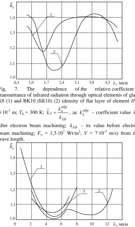
Resulting from the carried out researches it was determined (fig. 7, 8) that, as a result of electron beam processing of optical elements there is an increase in such an important optical characteristics that significantly affects the metrological characteristics of opto-electronic devices as transmittance factor of infrared radiation kλ
( )
λ (λ – wave length) in each range of infrared transparency of optical elements (table 2).For the elements of optical glass К8 and BK10 (БК10) the strongest increase of the coefficient kλ (for 20 ... 30%) is observed for the range changes λ = 0,76…2 μm and λ = 3…4 μm. For elements from optical ceramics КО1, КО2 иКО5 (values kλ for ceramic KO3 and KO12 remain unchanged) the strongest increase of the coefficient kλ (up to 30 ... 40 %) is observed for λ = 0,76…4 μm.
It is determined that = ≈
0 λ ∆
λ ∆ λ
∆ обр 1,08…1,15 (∆λобр,∆λ0
– for the elements, that are processed and not processed by electron beam электронным accordingly), so is observed small expansion range of infrared transparency of optical elements.
1 2
1 3
2,5 4
4 Ra, нм
1
2
Fn, 107Вт/м2
5,5 7
5
Fig.3. Height dependence of residual voids on the surface of elements of optical glass К8 (–––), TF110 (ТФ110) (– – –) and BK10 (БК10) (– ∙ – ∙) from the density of heat effect of electron beam for its different travel speeds: V= 5∙10-2 m/s (1); V= 8∙10-3
m/s (2) (∆, ○,□ – experimental data).
50
0 100 150
1
2
V, 103м/с
0 20 40 60 80
hпл, мкм
Fig. 4. The dependence of maximum thickness of melted layer in elements of optical glass BK10 (БК10) (1) and TF110 (ТФ110) (2) at Fп= 5∙108 Wt/m2 (–––) and Fп= 3∙108 Wt/m2 (– – –) from travelling speed of electron stream (∆, ○, □, ▲ – experimental data).
1 5,2
5,0 5,6
4 5,8
6,0
7 10 13
Нv, 10
3
МПа 1
2
5,4
5 4
3
Fn, 106Вт/м2 Fig.5. Dependence of microhardness surface of elements from optical ceramics КО12 (1), КО2 (2), КО1 (3), КО5 (4) и КО3 (5) at V= 7∙10-3 m/s (–––––) иV= 1,5∙10-2 m/s (– – –) from the density of heat effect of electron beam (∆, ○, □, ▲, ■, ♦, ▼, ●, ►, ◄ – experimental data).
1 100
75 150
4 175
200
7 10 13
∆,мкм
125
25 50
V, 103м/с
1 2
5 4
3
Fig. 6. The dependence of thickness toughened layers of elements from optical ceramics КО12 (1), КО2 (2), КО1 (3), КО3 (4) and КО5 (5) at Fп= 1,5∙107 Wt/m2 (–––––) and Fп= 2∙106 Wt/m2 (– – – ) from the travelling speed of electron beam (∆, ○, □, ▲, ■, ♦, ▼, ●, ►, ◄ – experimental data).
Table 1 The results of experimental data processing on the extension of lines on radiographs, mosaic block sizes (D) and change in the settings of a crystal lattice (Fп= 3∙106 Wt/m2, V= 3∙10-3 m/s)
Setting Coarse probe
Physical expansion of the two lines
Block size
D, А
Change in the settings of a crystal lattice
d d
∆ ∙10-4
Ceramics β1∙10
-3
, rad
2 β ∙10-3
, rad
КО1 1,472 1,734 1150 3,421
КО2 1,283 1,452 980 1,643
КО12 1,514 1,812 1240 3,810
КО3 1,120 1,320 890 1,225
КО5 1,132 1,289 760 1,117
Processed probe
КО1 0,687 0,231 4430 0,873
КО2 0,321 0,108 5250 0,291
КО12 0,746 0,254 4110 0,992
КО3 0,224 0,986 4210 0,193
КО5 0,589 0,637 5850 0,987
Table 2 IR transparencies of optical elements∆λ = λ2 – λ1 at Н= 4∙10
-3
m – for optical glass and Н = 10-2 m – for optical ceramics) Element material
∆λ, µm К8, BK10 КО1 КО2 КО5
0,3 1,1
1,0 1,3
1,0 1,4
1,7 2,4 3,1
kλ
2 1,2
1
λ, мкм
3,8 4,5
Fig. 7. The dependence of the relative coefficient of transmittance of infrared radiation through optical elements of glass К8 (1) and BK10 (БК10) (2) (density of flat layer of element Н =
4∙10-3
m; Т0= 300 К;
0 λ λ λ
k k k
обр
= , де kλобр – coefficient value kλ
after electron beam machining; kλ0 – its value before electron beam machining; Fn = 1,5∙107 Wt/m2, V = 7∙10-3 m/s) from the
wave length.
0 1,1
1,0 1,3
2 1,4
4 6 8
kλ
3 2
1,2
1
λ, мкм
10 12
Fig. 8. The dependence of the relative coefficient of transmittance of infrared radiation by optical elements from ceramics КО5 (1), КО2 (2) and КО1 (3) (density of flat layer of element Н = 10-2 m;
Т0= 300 К; Fn = 1, 5∙107 Wt/m2, V= 7∙10-3 m/s) from wave length.
Increase of transmittance of infrared radiation for elements from optical glass occurs as a result of reduction in the number and size of negative defects on the surface and in the
surface layers (scratches,
cracks, bumps, bubbles, depressions etc.) under the influence of the electron beam, which leads to their penetration. The consequence of this is a reduced number of residual voids h (nm) on their
surfaces and increase of the depth of melting hm (µm ) up to the
maximum permissible values of h*. Therefore there is a
one-to-one correspondence between the coefficient kλ and such important physico-mechanical properties of the surface layers of the elements as h and hm, which are presented in Fig. 9.
For items from optical ceramics the increase of kλ occurs as a result of the structural changes of the surface layers (increasing sizes of mosaic blocks, layers become more compact, etc.), resulting in an increase of microhardness of their surfaces Hv
and the formation of hardened layers having thickness ∆.
Therefore, there are also a one-to-one correspondence between the coefficient kλand parameters and Нv and ∆,
dependencies between which are presented in Fig. 10.
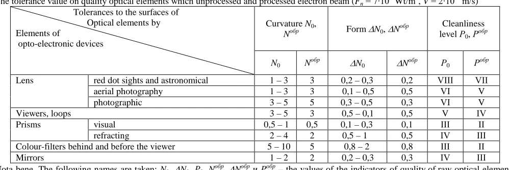
It is determined (table 3) that after finishing electron beam processing of surfaces of optical elements of the devices out of beam parameters installed for optimal ranges of their use, deviations from the geometrical form from configured match those accepted in opto-electronic tool engineering. Thereat the surface purity of optical elements in the class P after electron beam processing increases up to one grade of purity (e.g. for photographic lenses from class VI to class V; for mirrors – with IV to III, etc.).
As a result of electron-beam processing of optical elements without reflow occurs homogenization of chemical composition of the chemical composition of hydrolysis products (dissolution of K2O и Na2O at depth effects of the electron beam up
to 2...4 μm), which fill the defective surface layer, that remains after the standard mechanical processing, which leads to an improvement of the optical properties of the surface layers of the elements, namely to the reduction of their surface light scattering coefficient (wave length λ = 632,8 nm) (fig. 11).
In the result of the conducted research was outlined the influence of electron beam parameters to the coefficient kc: at the
increase of the parameter Fn from 7∙10
6
Wt/m2 to 3,9∙107 Wt/m2 and reduction of the parameter Vfrom 5∙10-2 m/s to 5∙10-3 m/s the value
kc decreases in 1,3...1,5 times. In addition, reduction of
the travelling speed of the electron beam leads to the increase of density influence of its thermal action in 1,2...1,3 times.
It is found out that the thermal action of the moving electron beam to the optical elements leads to their surface melting to a depth of 50 ... 200 μm, complete elimination of defective layers and reduction of micro relief of optical surfaces up to 0.5 ... 1 nm. The usage of masking and photo-and electron lithography enables create on the surface of optical elements functional micro-profiles in the form of grids, lattices, focusing lenses, and so on at a pitch of up to 100 µm.
1 0,8
0,7 0,9
5 10 15
2 1
20
kλ -1
h,нм 1
1,1
1,0 1,2
50 100 150
1
2
200 Область руйнування
1,3
*
kλ
hm,мкм h
a) b)
Fig. 9. The influence of residual voids h (а) and thickness of meltedlayer hm (б) to value kλ for the elements from optical glass BK10
(БК10) (1) and К8 (2) (λ= 1,06 µm).
Thus, in the light of modern technology used in optic-electronic tool engineering, electron beam processing of optical
elements is defined as potentially able to improve optical characteristics of elements of optoelectronic devices (increased transmittance of infrared radiation, light
scattering coefficient decrease of their surfaces, etc.), to increase their quality (compliance of geometric form with the configurated, increase of the purity and smoothness of the surface, etc.) as well as getting on the surface functional micro-profiles using electronic beams which can be used as the element base in microoptics, fiberoptics and integrated optics, optoelectronics, functional electronics etc.
In addition, the undeniable advantage of electron-beam technology is its environmental friendliness and ability
to obtain microelements with improved physicomechanical properties and optical characteristics, the use of which in opto-electronic devices helps to improve their metrological characteristics and reliability under harsh operating conditions, on the common board from optical material in a single technological cycle.
1,1
1,0 1,2
2 4
2 1
3
kλ
Нv, 10
3
МПа
Нv0 0
1,1
1,0 1,2
50 100 150
2
3
1
kλ
∆, мкм
a) b)
Fig. 10. The influence of microhardness of a surface Hv (а) and the thickness of the strengthened layers∆ (б) to value kλ for the elements
from optical ceramics КО5 (1), КО2 (2) and КО1 (3) (λ = 1,06 µm).
Table 3 The tolerance value on quality optical elements which unprocessed and processed electron beam (Fn= 7∙10
7
Wt/m2, V= 2∙10-3 m/s) Tolerances to the surfaces of
Optical elements by Elements of
opto-electronic devices
Curvature N0,
Nобр Form∆N0, ∆Nобр
Cleanliness level Р0, Робр
N0 Nобр ∆N0 ∆Nобр Р0 Робр
Lens red dot sights and astronomical 1 – 3 3 0,2 – 0,3 0,2 VІІІ VІІ
aerial photography 1 – 3 3 0,1 – 0,5 0,5 VІ V
photographic 3 – 5 5 0,3 – 0,5 0,3 VІ V
Viewers, loops 3 – 5 3 0,5 – 0,1 0,5 V ІV
Prisms visual 0,5 – 1 0,5 0,1 – 0,3 0,1 ІІІ ІІ
refracting 2 – 4 2 0,5 – 1 0,5 ІV ІІІ
Colour-filters behind and before the viewer 5 – 10 5 0,8 – 2 0,8 ІІІ ІІ
Mirrors 1 – 2 2 0,2 – 0,3 0,3 ІV ІІІ
Nota bene. The following names are taken: N0, ∆N0, Р0, Nобр, ∆NобриРобр – the values of the indicators of quality of raw optical elements
and processed by electronic beam, respectively.
4. Conclusions
1. New experimental data is obtained on the influence of electron beam parameters on physico-mechanical properties of the surface layers of optical elements: optimal ranges of density of heat ray, and the speed of its movements are defined, within which there is maximum improvement (more than 3 ... 5 times) of basic properties (reduction of the area of negative defects on the surface, etc.), decrease of residual voids onn the surface, increase in its microhardness, formation of hardened layers, etc.) that allows to increase the stability of the external elements to thermal and mechanical influences, thus increasing the reliability of the devices.
2. For the first time it is determined, that by controlling the physical and mechanical properties of the surface layers of optical elements using a mobile electron beam it is possible to improve optical characteristics: increase the transmittance of infrared radiation and reduce the coefficient of light scattering of surfaces of elements) that allows to improve metrological characteristics of optoelectronic devices.
3. It is defined that after finish electron beam processing of the surfaces of optical elements of devices, variations in their geometric form from the specified match those accepted forms in
optical-electronic tool engineering, and the purity of elements’ surface in class P increases for lenses from VI to class V; for eyepieces from V to IV class; for prisms and mirrors – class IV to III, which increases the metrological characteristics and reliability of devices by their operation.
0,7 0,6
0,5 0,8
1,5 0,9
2,3 3,1 1
2
0,7
Fn, 107
Вт/м2 kc
Fig. 11. Dependence of relative light scattering coefficient of working surfaces of optical elements from glass К108 (1) и BK10 (2) the density of thermal action of electron beam for different speeds of its movement (the thickness of a flat layer of the
element Н= 4∙10-3 m; Т0= 300 К; 0
c c c
k k
k = , where kc – current
value; kc0 – value kc under Fn= 7∙106 Wt/m2): ––– – V =
5∙10-2
m/s; – – – – V= 5∙10-3 m/s.
5.
References
1. Яценко И. В. Упреждение возможных разрушений
оптических обтекателей ИК-приборов в условиях выстрела и
полета // Ежемесячный научно-технический и
производственный журнал “Наноинженерия”, 2015. – № 12(54). – С. 26 – 31. (Яценко И. В., Антонюк В. С.,Ващенко В. А., Цыбулин В. В.)
2. Яценко І. В.Попередження можливих руйнувань оптичних
елементів точного приладобудування в умовах зовнішніх термодій // Журнал нано- та електронної фізики, 2016. – т. 8. – № 1. – С. 01027 – 01032. (Яценко І. В., Антонюк В. С., Ващенко В. А., Цибулін В. В.)
3. Яценко І. В. Визначення критичних значень параметрів зовнішніх термодій на оптичні елементи точного
приладобудування // Вісник Національного технічного
університету України “Київський політехнічний інститут”, 2016. – № 51(1). – С. 71 – 75. (Яценко І. В., Антонюк В. С., Кириченко О. В., Ващенко В. А.)
4. Яценко І. В. Визначення критичних значень параметрів електронного променю при поверхневому оплавленні оптичних елементів точного приладобудування // Журнал нано- та
електронної фізики, 2017. – т. – № 1. – С. . (Яценко І. В., Антонюк В. С., Ващенко В. А., Цибулін В. В.)
5. Ващенко В. А. Основи електронної обробки виробів з оптичних матеріалів. Монографія. – К.: Наукова думка, 2011. –
562 с. (Ващенко В. А., Яценко І. В., Лега Ю. Г, Кириченко О. В.)
6. Яценко І. В. Дослідження залежностей енергетичних
характеристик СЕП від його керованих параметрів при впливі на вироби мікрооптики і інтегральної оптики // Сб. “Труды
Одесского политехнического университета”, 2009. – вып. 2(32). – С. 143 – 149.
7. Yatsenko І. V. Experimental and statistical models of impact determination of the electron beam parameters on surface layers properties of optical elements in precision instruments building // “Pratsi. Odes’kyi politechnichnyi universytet”, 2016. – Issue 1(48). – P. 63 – 69.
8. Yatsenko I. Influence of parameters by electronic ray on properties of superficial layers of optical elements of exact instrument-making // International journal for science and
innovations for the industry “Innovations in discrete productions”, ISSN 114-8907, YEAR III, ISSUE 1/2015, Sofia. – P. 13 – 15. (Yatsenko I., Antoniuk V., Bondarenko M., Vashchenko V.)
9. Yatsenko I. Improvement of technical and operational characteristics of devices with optical elements by preliminary electron beam treatment of their surface // International journal for science and innovations for the industry “Machines. Technologies. Materials”, ISSN 1313-0226, YEAR X, ISSUE 6/2016, Bulgaria. –
P. 47 – 50. (Yatsenko I., Antoniuk V., Kiritchenko O., Vashchenko V.)
10.Yatsenko I. Increasing the resistance of precision instrument-making elements from optical glass to external thermo-influences by preliminary electron-beam processing of surfaces // International journal for science and innovations for the industry “Innovations in discrete productions” ISSN 1314-8907, YEAR IX, ISSUE 1/2016, Bulgaria. – P. 9 – 12. (Yatsenko I., Antoniuk V., Kiritchenko O., Vashchenko V., Tsybulin V.)
11.Yatsenko I. Improving the reliability instruments of measuring and thermal control of objects of different physical nature by the finish of electron beam processing surfaces of optical elements // International journal for science and innovations for the industry “Innovations in discrete productions” ISSN 1314-8907, YEAR X, ISSUE 2/2016, Bulgaria. – P. 11 – 14. (Yatsenko I., Antoniuk V., Kiritchenko O., Vashchenko V., Tsybulin V.)
12.Антонюк В. С. Підвищення фізико-механічних параметрів
елементів з оптичних керамік фінішною електронно
-променевою обробкою // Сучасні технології в
машинобудуванні. Збірник наукових праць. – Харків: НТУ “ХПІ”, 2016. – Вип. 11. – С. 74 – 86. (Антонюк В. С., Яценко І. В., Кириченко О.В., Ващенко В. А.)
13.Яценко І. В. Покращення техніко-експлуатаційних характеристик приладів з оптичними елементами шляхом збільшення їх коефіцієнта пропускання ІЧ-випромінювання // Сб. Инженерия поверхности и реновации изделий. Материалы 16 Международной научно-техническойконференции, 29 – 31 травня 2016 г, г. Затока – Київ: АТМ України. – С. 185 – 187.
(Яценко І. В., Антонюк В. С., Кириченко О. В., Ващенко В. А.)
14.Яценко І. В. Підвищення метрологічних характеристик та надійності приладів для вимірювання та теплового контролю
об’єктів різної фізичної природи шляхом електронно
-променевої обробки їх оптичних елементів // Матеріали ІІ
Всеукраїнської науково-практичної конференції
“Приладобудування та метрологія: сучасні проблеми, тенденції розвитку”, 6 – 7 жовтня 2016 р., м. Луцьк. – С. 100 – 101. (Яценко І. В., Антонюк В. С.,Гордієнко В. І., Кириченко О.В., Ващенко В. А.)
15.Окатов М. А. Справочник оптика-технолога. – СПб.: Политехника, 2004. – 679 с. (Окатов М. А., Антонов Э. А., Байгожин А. Б.)
16.Зверев В. А. Оптические материалы. Учебное пособик для конструкторов оптических систем и приборов. – СПб.: Издательство СП НИУИТМО, 2009. – 243 с. (Зверев В. А., Кривопустова Е. В., Точилина Т. В.)
17.ГОСТ 11141-84. Детали оптические. Классы чистоты поверхностей. Методы контроля.
18.Вильчинская С. С. Оптические материалы и технологии – Томск: Изд. Томского политехнического университета, 2011. – 107 с. (Вильчинская С. С., Лисицын В. М.)
.