ISSN: 2231-5381
http://www.ijettjournal.org
Page 169
Designing and Parametric Variation of
PI Controller for Buck Converter for Constant
Voltage Applications
Sugandhra Pal Singh#1, Deepak Kumar Singh*2, Harish Kumar$3, Rheesabh Dwivedi^4
#
M.Tech Scholar, Department of Electrical and Electronics Engineering, Bhagwant Institute of Technology, Muzaffarnagar, Uttar Pradesh, India
*,^
Assistant Professor, Department of Electrical Engineering, Teerthanker Mahaveer University, Moradabad, Uttar Pradesh , India
$
Professor, Department of Electronics and Communication Engineering, Bhagwant Institute of Technology, Muzaffarnagar, Uttar Pradesh, India
Abstract- In this paper, we study on buck dc/dc converter of high
efficiency by soft switching technique. The paper will focus on modeling, analysis, and design and simulation buck converter architecture. The converter is designed in CCM (continuous conduction mode). The voltage mode control strategy is proposed by using pulse width modulation
(PWM) with a proportional-integral (PI). The
effectiveness of the step down converter is verified through simulation results using control oriented simulator like MATLAB/Simulink tools. The circuit operation, designs and simulation results are mentioned in this paper.
Keywords
—Buck Converter, Total Harmonic Distortion,
Pulse width modulation and PI control.
I. INTRODUCTION
DC-DC converters are some of the simplest power circuit. It is a device which transforms AC to DC. This device is also known as an AC to DC converter. A Chopper can be considered as a DC equivalent of an AC transformer with a convertible constant convertible in a continuous form. Like a transformer, the converter can be employed for stepwise increase or reduction of DC source voltage.
The name Buck Converter most probably evolves from the fact that the input voltage is bucked/chopped or attenuated, in amplitude and a lower amplitude voltage appears at the output. This paper discusses the design of an optimized controller and a buck converter, while presenting the result of analysis.
II. OPERATION CIRCUIT MODEL FOR BUCK
CONVERTER
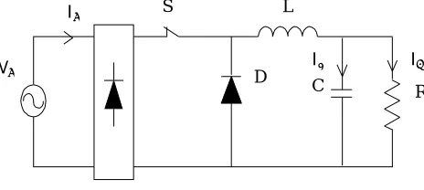
Figure 1 shows the DC-DC Buck Converter circuit topology. The circuit operation can be divided into two modes.
Mode 1 (Switch is closed):
When the controlled switch (e.g. MOSFET) ‘S’ is on by by pulse width modulation (PWM), then input voltage appears across the inductor L, filter capacitor, C and load resistor R and current in inductor L increases linearly. In the same cycle the capacitor C is charged. During mode 1, the diode reversed biased and resulted from flowing current, the input provides energy to the load as well as to the inductor.
Mode 2 (Switch is open):
When the controlled switch i.e MOSFET is switch off. The voltage across the inductor L is reversed. However, current in the inductor L cannot change instantaneously and the current starts decreasing linearly through inductor L capacitor C, load R and diode D. In this cycle the capacitor is also charged with the energy stored in the inductor.
I S
D
I
R
I
L
C
Figure 2. Mode:1 When switch is closed
V
I S
D
I
R
I
L
C
Figure 1. DC-DC Buck converter
ISSN: 2231-5381
http://www.ijettjournal.org
Page 170
A. Design parameter and equations for buck converter:
V = DV
L= (1− )/(∆ )
C
= (1-D)/(8 )(∆ / )Where
f
= switching frequency∆
I
= Peak to Peak ripple currentI
(assuming 10% ofI
)∆
V
= voltage ripple (assuming 5% ofV
) D = Duty cycle.B. The calculated value of Buck converter:
Input voltage (
V
) = 220 volts Output voltage (V
) = 48 volts Duty cycle (D) = 21.81%Switching frequency (fs) = 25 kHz
Inductor (
L
) = 7.8 mH Capacitor (C
) = 0.434 µFThe results of open loop buck converter is shown in figure 5, which depicts peak to peak ripple voltage (∆Vo) is 8.6 Volt and maximum o v e r s h o o t of 1 7 . 3 %. Since the design equations assume constant input voltage and constant load under steady state conditions, the variation of input voltage shall result in fluctuation in output Therefore, a closed loop controller is required with optimized parameters to suit the constant voltage output as per requirement of load.
C. Controller for closed loop buck converter give design equations:
The Simulink Schematic of buck converter with analog PI controller is shown in figure 6.
The output voltage is sensed Vout and compared with the
input voltage Vref then an error signal is produced which
is processed through PI controller to generate a control voltage. The control voltage is used to feed to the PWM generator for control of switch. The PI controller has two parameters namely KP and KI.
PI controller has transfer function:C(s) = + Where, =Proportional gain and = Integral gain. The results of closed loop flyback converter is shown in fig.7 powergui
Discrete, Ts = 1e-006 s.
v +
-Voltage Measurement
v +
-Universal Bridge
A
B +
-Scope 2 Scope 1
R Load Pulse
Generator
Mosfet
g
D S
L
Diode
Current Measurement
i +
-C1 C
0 0.05 0.1 0.15 0.2 0.25 0.3 0.35 0.4 0
10 20 30 40 50 60
powergui Discrete, Ts = 1e-006 s.
v +
-Universal Bridge A
B +
-Scope PWM Control
In1 Out1 Out2 PI Controller
PI Mosfet
g D
S
L
Diode
Current Measurement i +
-Constant 48
C1 C
Load
I S
D
R
I
C
Figure 3. Mode:2 When switch is open
Figure 4. Simulation model of buck converter for open loop control
Figure 6. Simulation model of buck converter for closed loop control
I
V
L
Time (Secs)
V
(V
o
lt
s)
ISSN: 2231-5381
http://www.ijettjournal.org
Page 171
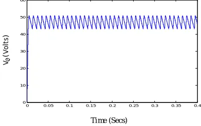
which has maximum overshoot of 12.72%, settling time 0.01sec and rise time 0.01 sec.
III. EFFECT DUE TO VARIATION OF KP AND KI ON OUTPUT VOLTAGE AND INDUCTOR CURRENT
TABLE I Performance parameters when L=7.8 mH, C= 0.434 µF, K= 20 and value of K is varied
K Voltage(V ) Current (I )
O.S (%) Settling Time Rise Time O.S (%) Settling Time Rise Time
0.04 32.08 0.01 0.01 32.29 0.01 0.01
0.10 19.79 0.01 0.01 21.42 0.01 0.01
0.16 12.72 0.01 0.01 13.89 0.01 0.01
0.22 14.58 0.01 0.01 14.28 0.01 0.01
0.28 12.5 0.01 0.01 14.28 0.01 0.01
(a) Performance of output voltage (V) Vs time graph for flyback converter when K value is varied.
0 0. 05 0.1 0. 15 0.2 0. 25 0.3 0.35 0.4 -10
0 10 20 30 40 50 60
0 0.05 0. 1 0. 15 0. 2 0. 25 0.3 0.35 0.4 0
0. 5 1 1. 5 2 2. 5
0 0. 05 0.1 0.15 0.2 0.25 0.3 0.35 0.4 -10
0 10 20 30 40 50 60
0 5 10 15 20
0 20 40
%
O
v
er
S
h
o
o
t
Kp
0 0.002 0.004 0.006 0.008 0.01 0.012
0 20 40
S
et
tl
in
g
T
im
e
(S
ec
s)
Kp
0 0.002 0.004 0.006 0.008 0.01 0.012
0 20 40
R
is
e
T
im
e
(S
ec
s)
Time (Secs)
V
(V
o
lt
s)
I
(A
m
p
er
e
)
Time (Secs)
Figure 7. Closed loop response of Output voltage Vs Time
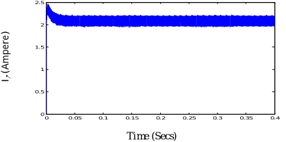
Figure 8. Closed loop response of Inductor current (I) Vs Time
V
(V
o
lt
s)
Time (Secs)
Figure 9. Output voltage Vs time with K = 0.16
Figure 10. Effect on overshoot due to variation in K
Figure 11. Effect on settling time due to variation in K
K
ISSN: 2231-5381
http://www.ijettjournal.org
Page 172
(b) Performance of magnetization current (I ) Vs time graph for buck converter when K value is varied.
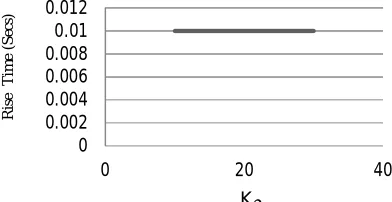
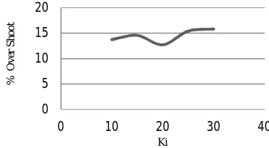
TABLE II Performance parameters when L= 7.8 mH, C = 0.434 µF,K = 0.16, K value is varied .
K Voltage(V ) Current (I )
O.S (%) Settling Time Rise Time O.S (%) Settling Time Rise Time
10 13.75 0.01 0.01 16.66 0.01 0.01
15 14.58 0.01 0.01 16.91 0.01 0.01
20 12.72 0.01 0.01 13.89 0.01 0.01
25 15.41 0.01 0.01 17.61 0.01 0.01
30 15.83 0.01 0.01 18.09 0.01 0.01
(a) Performance of output voltage (V) Vs time graph for buck converter when K value is varied.
0 0.05 0.1 0.15 0.2 0.25 0.3 0.35 0.4 0
0.5 1 1.5 2 2.5
0 5 10 15 20
0 10 20 30 40
%
O
v
er
S
h
o
o
t
Kp
0 0.002 0.004 0.006 0.008 0.01 0.012
0 20 40
S
et
tl
in
g
T
im
e
(S
ec
s)
Kp
0 0.002 0.004 0.006 0.008 0.01 0.012
0 10 20 30 40
R
is
e
T
im
e
(
S
ec
s)
0 0. 05 0.1 0.15 0.2 0.25 0.3 0.35 0.4 -10
0 10 20 30 40 50 60
0 5 10 15 20
0 10 20 30 40
%
O
v
er
S
h
o
o
t
Ki
I
(A
m
p
er
e
)
Time (Secs)
Figure 13. Magnetization current (I ) Vs time with K = 0.16 Figure 14. Effect on overshoot due to variation in K
V
(V
o
lt
s)
Time (Secs)
Figure 17. Output voltage Vs time with K = 20 Figure 18. Effect on overshoot due to variation in K
Figure 15. Effect on settling time due to variation in K
K
ISSN: 2231-5381
http://www.ijettjournal.org
Page 173
(b) Performance of inductor current (I ) Vs time graph for buck converter when K value is varied.
IV. CONCLUSION
Step down switching regulators are the backbone of electronic equipments. The designing of buck converters has been carried out for constant voltage applications considering KP
and KI are the performance parameter for PI controller. Buck
converter has been designed to deliver 48 volts DC to a 100 watt load. Performance and applicability of this converter is presented on the basis of simulation in MATLAB SIMULINK. Buck converters are employed for low power applications below 150 W and with voltages below 230V. The parametric variation analysis of buck converter have been carried out for constant voltage applications considering
The design concepts are validated through simulation and results obtained show that a closed loop system using buck converter will be highly stable with high efficiency. Better efficiency due to: moderate duty cycles, lower voltage MOSFETs and rectifiers, and reduced switching losses due to reduced peak-to-peak voltage swing.
REFERENCES
[1] Sanjeev Singh and Bhim Singh, “Comprehensive study of single-phase AC-DC power factor corrected converters with high-frequency isolation” IEEE Trans. on Industrial Informatics, vol. 7, no. 4, Nov. 2011, , pp. 540-556.
0 0.005 0.01 0.015
0 10 20 30 40
S
et
tl
in
g
T
im
e
Ki
0 0.005 0.01 0.015
0 10 20 30 40
R
is
e
T
im
e
Ki
0 0.05 0.1 0.15 0.2 0.25 0.3 0.35 0.4 0
0.5 1 1.5 2 2.5
0 5 10 15 20
0 10 20 30 40
%
O
v
er
S
h
o
o
t
Ki
0 0.005 0.01 0.015
0 10 20 30 40
S
e
tt
li
n
g
T
im
e
Ki
0 0.005 0.01 0.015
0 10 20 30 40
R
is
e
T
im
e
Ki
Figure 19. Effect on settling time due to variation in K Figure 20. Effect on rise time due to variation in K
I
(A
m
p
er
e
)
Time (Secs)
Figure 21. Magnetization current (I ) Vs time with K = 20
Figure 23. Effect on settling time due to variation in K Figure 24. Effect on rise time due to variation in K
ISSN: 2231-5381
http://www.ijettjournal.org
Page 174
[2] Sanjeev Singh and Bhim Singh, “Power quality improved PMBLDCM drive for adjustable speed application with reduced sensor buck-boost PFC converter” in proc. IEEE 11th ICETET, 2011, pp.180-184.
[3] Boopathy.K and Dr.Bhoopathy Bagan .K, “Buck Boost converter with improved transient response for low power applications” in Proc. IEEE SIEA, Sep 2011, pp. 155-160.
[4] Altamir Ronsani and Ivo Barbi, “Three-phase single stage AC-DC buck-boost converter operating in buck and buck-boost modes” in Proc. IEEE, 2011, pp.176-182.
[5] Sanjeev Singh and Bhim Singh, “An adjustable speed PMBLDCM drive
for air conditioner using PFC Zeta converter,” Int. J. Power Electron.
(IJPElec), vol. 3, no. 2, pp. 171–188, Apr. 2011.
[6] B. Singh, B. N. Singh, A. Chandra, K. Al-Haddad, A. Pandey, and D. P. Kothari, “A review of single-phase improved power quality ac–dc
converters,” IEEE Trans. Ind. Electron., vol. 50, no. 5, pp. 962–981, Oct.
2003.
[7] Sanjeev Singh and Bhim Singh, “Single-phase power factor controller topologies for permanent magnet brushless DC motor drives,” in IET Power Electron., 2010, Vol. 3, Iss. 2, pp. 147–175.
[8] Sanjeev Singh and Bhim Singh, “A voltage controlled adjustable speed PMBLDCM drive using a single-stage PFC half-bridge converter,” in
Proc.IEEE APEC’10, 2010, pp. 1976–1983.
[9] S. C. Raviraj and P. C. Sen, “Comparative study of proportional-integral, sliding mode, and flay logic controllers for power converters,” IEEETransactions on Industrial Applications, vol 33, no.2, pp.518— 524, MariApr. 1997.
[10] Sanjeev Singh and Bhim Singh, “Power quality improved PMBLDCM
drive for adjustable speed application with reduced sensor buck-boost PFC converter” in proc. IEEE 11th ICETET, 2011, pp.180-184.
[11] Venkstarsmanan, A. Sabanoivc, and S. Culç “Sliding mode control of dc-to-dc converters,” in Proc. IEEE ConE Industrial Electronics, Control Instnjmentations (IECON), pp. 25 1-258, 1985.
[12] M. Namnabat, M. Baysti Poodeh, S. Eshlehardiha, “Comparison the