Photon Counting Detector For Space Use
Michael Leonard Edgar
Milliard Space Science Laboratory Department of Physics and Astronomy
University College London
Submitted to the University of London for the degree of Doctor of Philosophy
All rights reserved
INFORMATION TO ALL U SE R S
The quality of this reproduction is d ep en d en t upon the quality of the copy subm itted.
In the unlikely even t that the author did not sen d a com plete manuscript
and there are m issing p a g e s, th e se will be noted. Also, if material had to be rem oved, a note will indicate the deletion.
uest.
ProQ uest 10105611
Published by ProQ uest LLC(2016). Copyright of the Dissertation is held by the Author.
All rights reserved.
This work is protected against unauthorized copying under Title 17, United S ta tes C ode. Microform Edition © ProQ uest LLC.
ProQ uest LLC
789 East E isenhow er Parkway P.O. Box 1346
This thesis describes the development of a microchannel plate (M CP) based photon counting detector using the Spiral Anode (SPAN) as a readout. This detector was one of two being evaluated for use in the Optical Monitor for ESA’s X-ray Multi Mirror satellite. Throughout this thesis, where possible, the underlying physical processes, particularly those of the MCP, have been identified and studied separately.
The first chapter is an introduction to photon counting detectors and includes a review of the various readouts used with MCPs. The second chapter provides a more detailed review and analysis of cyclic, continuous-electrode, charge-division readouts, of which SPAN is an example.
The next two chapters describe the technique for measuring the radial distribution of the MCP charge cloud, which can significantly affect detector imaging performance . Results are presented for various operating conditions. The distribution consists of two parts and the size is dependent on the operating voltages of the MCP stack.
The fifth and sixth chapters describe the procedure for operating a SPAN read out and the decoding necessary for converting the ADC readings into a two dimensional coordinate. Various methods are described and their limitations evaluated. The cause of problems associated with the SPAN readout, such as “ghosting” and fixed patterning and methods of reducing them are discussed in detail. Results are presented which demonstrate the performance of the anode.
The seventh chapter discusses and evaluates the interaction between channels in MCPs and the long range effects an active pore has on the surrounding quiescent pores. This represents the first time that these effects have been measured. The importance of this phenomenon for imaging detectors is discussed and possible mechanisms evaluated.
For nation shall rise against nation and kingdom against kingdom: and there shall be famines, and pestilences, and earthquakes in diverse places.
A ll these are the begining of sorrows.
Then shall they deliver you up to be afflicted, and shall kill you:...
A nd then shall many be offended, and shall betray one another, and shall hate one another. And many false propets shall rise, and shall decieve many.
A nd because iniquity shall abound, the love of many shall wax cold. But he that shall endure unto the end, the same shall be saved.
A b s tr a c t 2
L ist o f F ig u re s 9
L ist o f T ab les 15
1 R e v ie w o f T w o D im e n sio n al P h o to n C o u n tin g D e te c to rs 16
1.1 MicroChannel Plate, Secondary Electron M u ltip lie r s ... 19
1.1 . 1 Electron Multiplication in M C P s ... 23
1.1 . 2 Ion F e e d b a c k ... 25
1.1.3 S a tu ra tio n ... 28
1.1.4 Gain Depression with Count R a t e ... 31
1 . 2 MCP Based P h o to m u ltip liers... 35
1.2.1 EUV and X-Ray P h o to m u ltip lie rs... 35
1.2 . 2 Optical/UV P h o to m u ltip liers... 35
1.3 MCP Position R e a d o u ts ... 39
1.3.1 Light Amplification D e tec to rs... 39
1.3.2 Charge Measurement D e tec to rs... 45
1.4 An Optical Monitor for the XMM S a t e l l i t e ... 59
1.4.1 Detectors... 60
2 C y clic C o n tin u o u s E le c tro d e C h a rg e M e a s u re m e n t D ev ices 63 2 . 1 Fine P o s itio n ... 65
2.1.1 Analysis of Sinusoidal E le c tro d e s... 65
2.1.2 The Effect of the Phase Angle ... 6 6 2 . 2 Coarse P o s itio n ... 71
2.2 . 1 The Double Diamond C a t h o d e ... 71
2.2.2 The Vernier A n o d e ... 73
2.2.3 The Spiral Anode (S P A N )... 73
2.3 Practical A n o d e s ... 76
3.3.1 Electronics and D ata A cqu isition... 87
3.4 Analysis of the S c u rv e ... 87
3.4.1 The Probability Density Distribution of the One Dimensional Inte grated Charge C lo u d 87 3.4.2 The Structure and Reduction of the S c u rv e ... 8 8 3.4.3 Qualitative Discussion of the Charge Cloud Using p { c p )... 92
3.5 Determining The Radial Distribution of the Charge C lo u d ... 95
3.5.1 Necessary Conditions for Determining the Radial Distribution of the Charge C lo u d ... 95
3.5.2 The In versio n... 95
3.5.3 The Least Squares P ro b le m ... 1 0 0 3.5.4 The Linear Least Squares S o lu tio n ... 101
3.5.5 The Radial Probability D is trib u tio n ... 1 0 2 3.6 The Nonlinear Leaat Squares P r o b le m ... 103
3.6.1 A Manual Search In Three D im e n sio n s... 103
3.6.2 Methods for Minimizing a V ariab le... 105
3.6.3 Powell’s Method of Conjugate Directions ... 106
3.7 Practical C onsiderations... 108
3.7.1 Accuracy and S tab ility ... 109
M e a s u re m e n ts o f th e R a d ia l D is trib u tio n o f th e C h a rg e C lo u d . 113 4.1 Range of M ea su rem en ts... 113
4.1.1 Range of Measurements at an MCP Anode Gap of 6.2 m m ... 113
4.1.2 Range of Measurements at an Anode Gap 3.0 m m ... 115
4.2 The General Form of the Radial Distribution of the Charge C l o u d ... 115
4.2.1 The Two Component Nature of The Radial D istrib u tio n ... 115
4.2.2 The Form of the Central C om ponent... 118
4.2.3 The Form of the Wing C o m p o n e n t... 119
4.3 The Size of the Radial D istrib u tio n ... 125
4.3.1 The Fit Parameters and the Radial D is tr ib u tio n ... 125
4.3.2 The Fit Parameters at an Anode Gap of 6 . 2 m m ... 126
4.3.3 The Fit Parameters at an Anode Gap of 3.0 m m ... 131
4.3.4 A Simple Ballistic M o d e l ... 131
4.3.5 Space C h a rg e ... 138
4.4 The Variation of Charge Cloud Size with MCP Operating Conditions. . . . 138
4.4.1 The Effects of Gain on Charge Cloud S iz e ... 138
4.4.2 The Effects of Eg on Charge Cloud S i z e ... 144
4.4.3 Plate Bias V oltage... 144
4.4.4 Comparison of the Measurements for the Two Gaps... 149
4.4.5 The Effect of the Inter-plate Gap V o lta g e ... 152
4.5 Charge Cloud Sym m etry ... 153
4.5.1 E U ip ticity ... 153
5.1.1 Coordinate R o ta tio n ... 161
5.1.2 Transformation to Cylindrical Polar C o o rd in a te s ... 163
5.1.3 Normalization W ith Respect to Pulse H e i g h t ... 165
5.1.4 Spiral Arm Assignment by Linear Discriminant A nalysis... 166
5.1.5 G h o sts... 169
5.2 Radius as a Function of Pulse H e ig h t... 169
5.2.1 The Cause of Variation of Radius with Respect to Pulse Height . . 174
5.2.2 Correction of Radius W ith Respect to Pulse Height ... 180
5.2.3 Limitations on the C o rrectio n... 182
5.3 Determining Spiral Constants ... 182
5.3.1 Line Finding by Edge D e t e c t i o n ... 185
5.3.2 The Hough T ra n sfo rm ... 192
5.3.3 C om parison... 199
5.3.4 Variation of Spiral C o n s ta n ts ... 203
5.4 Spiral Arm Assignment by Statistical Distribution of p In Hough Space . . 206
5.5 Applications for Other D e te c to r s ... 208
5.6 How the Algorithm is Im plem ented... 211
5.7 SPAN Imaging P erform ance... 213
5.7.1 Pulse Height Related Position S h i f t s ... 213
5.7.2 Positional Linearity and R esolution... 214
6 T h e E ffects o f D ig itiz a tio n fo r t h e S P A N R e a d o u t 220 6 . 1 The Effects of Anode Design Parameters on Fixed P a tte rn in g ... 225
6 . 2 The Effects of User Defined Parameters on Fixed P a t t e r n i n g ... 226
6.2.1 Pulse Height Related Vignetting... 229
6.3 Fixed Reference A D C s ... 230
6.4 Ratiometric A D C s ... 237
6.5 A lia s in g ... 240
6 . 6 Chicken Wire D is to rtio n ... 243
6.7 Possible Techniques for Reducing Fixed P a tte rn in g ... 243
7 T h e L ong R a n g e I n te ra c tio n B e tw e e n P o re s 248 7.1 In tro d u ctio n... 248
7.1.1 A djacency... 248
7.1.2 Effects of Gain D epression... 251
7.2 Experimental P ro c e d u re ... 252
7.2.1 MCP C o n fig u ra tio n ... 254
7.2.2 Readout and E lectronics... 255
7.2.3 Softw are... 255
7.3 The Spatial Extent of Gain D epression... 256
7.4 Measurements of the Long Range Effects of Gain D e p re s s io n ... 260
7.4.1 Further Measurements with the Pin H o l e ... 261
R i n g ... 269
7.6 Long Term, Long Range Gain D e p re s s io n ... 271
7.6.1 The Variation of Long Term, Long Range Gain Depression with Time 276 7.6.2 The Variation of Long Term, Long Range Gain Depression with Plate V o lta g e ... 282
7.6.3 Image Distortions Due to the Long Term Effects of Long Range Gain Depression ... 285
7.7 Possible Mechanisms for Long Range Gain D e p re ssio n ... 289
7.7.1 Dynamic, Long Range Gain D e p re s s io n ... 289
7.7.2 Long Term, Long Range Gain D e p re ssio n ... 294
7.7.3 C o n c lu s io n ... 299
8 C o n clu sio n s a n d F u tu r e W o rk 300 8 . 1 The Size of the Charge C lo u d ... 300
8 . 2 The Interaction Between P o r e s ... 302
8.3 The Spiral A n o d e... 304
8.3.1 Problems with SPAN ... 305
8.3.2 Proposed Real Time Operating S y s te m s ... 306
8.3.3 The Analogue Front E n d ... 310
8.3.4 The Suitability of SPAN for Use in S p a c e ... 310
B ib lio g ra p h y 313
1 . 1 Spatial and energy resolution for various two dimensional photon counters. 17 1 . 2 Schematic diagram of an MCP... 2 0
1.3 The variation of element composition with depth in the glass material after reduction... 2 2
1.4 The variation in the yield of secondary electrons with varying primary elec tron energy for the glass after reduction... 2 2
1.5 The relation between gain and Vd... 26
1 . 6 Universal gain curve of an MCP... 26
1.7 Schematic diagram of a Chevron pair MCP configuration combined with a Wedge and Strip Anode... 29
1 . 8 PHDs demonstrating different levels of saturation... 29
1.9 The variation of the electric field within a channel with increasing saturation. 30 1 . 1 0 The reduction of the secondary emission coefficient, 6, with surface charging for reduced lead glass... 30
1.11 PHDs exhibiting various degrees of gain depression with variation on count ra te... 32
1.12 Gain depression with count rate with high resistance plates... 34
1.13 UV Quantum Efficiency of MCP m aterial... 36
1.14 Quantum Efficiency of an S20 photocathode... 36
1.15 Schematic diagram of a sealed tu b e... 38
1.16 Proximity focussing PSF FW HM... 38
1.17 Schematic diagram of the PAPA detector... 41
1.18 Three and five point centroiding for the MIC detector... 44
1.19 Schematic Diagram of the MAMA detector... 48
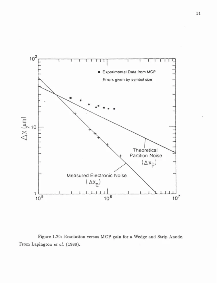
1 . 2 0 Resolution versus MCP gain for a Wedge and Strip Anode... 51
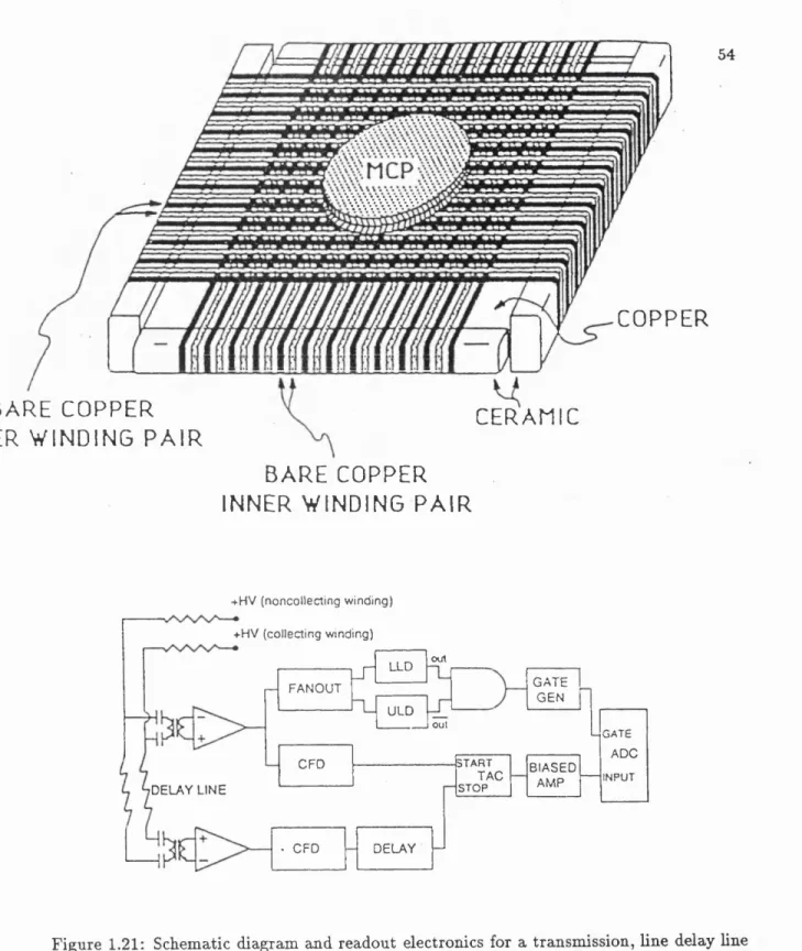
1 . 2 1 Schematic diagram and readout electronics for a transmission, line delay line readout... 54
1 . 2 2 Schematic diagram of a WSA... 58
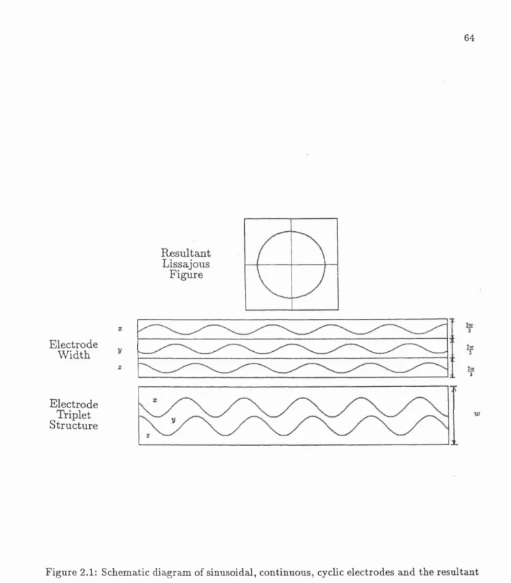
2 . 1 Schematic diagram of sinusoidal, continuous, cyclic electrodes and the resul tant Lissajous figure... 64
2.3 The Euler angles for a rotation through three dimensions... 67
2.4 Schematic diagram of the Double Diamond readout. ... 72
2.5 Schematic diagram of the Vernier anode... 72
2 . 6 The evolution of the spiral with movement along the anode... 75
2.7 The differential increase of arc length for a curve... 76
2 . 8 Schematic diagram of the one dimensional SPAN readout for the SOHO satellite... 78
2.9 Schematic diagram of a two dimensional SPAN... 78
3.1 An example of measured and simulated modulation for a WSA... 80
3.2 Measured S-distortion for a WSA... 82
3.3 O utput from the double diamond cathode showing the effects of the convo lution of the charge cloud with the geometry of the electrodes... 82
3.4 Schematic diagram of the Split Strip anode... 84
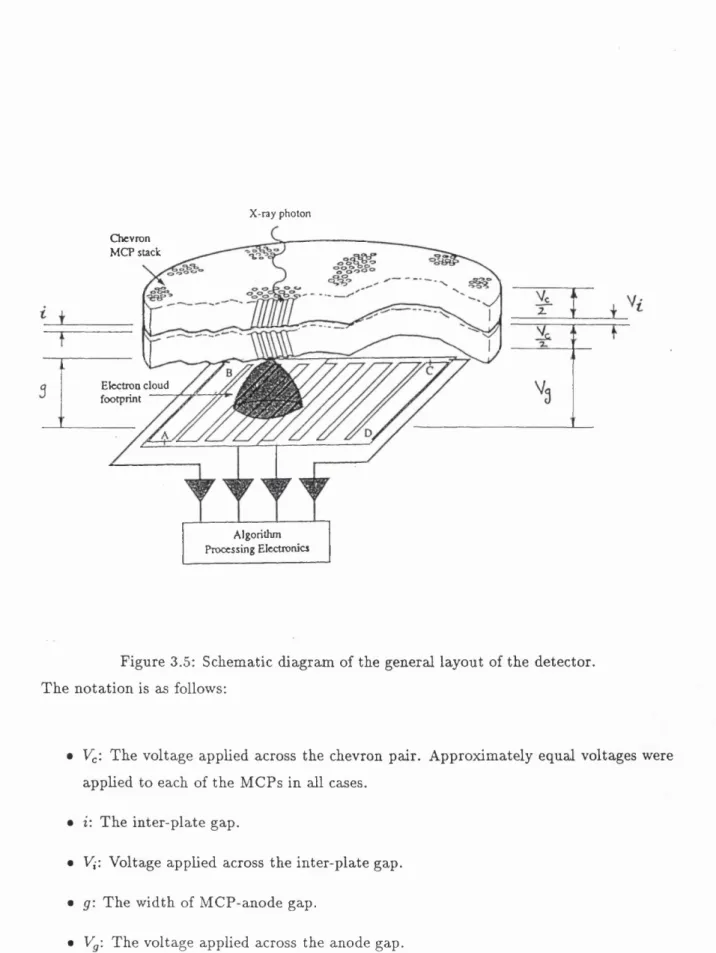
3.5 Schematic diagram of the general layout of the detector... 85
3.6 The S curve returned by the Split Strip anode... 8 6 3.7 The probability density distribution of the integrated one dimensional dis tribution, p{cp) of the charge cloud obtained from the d ata represented in Figure 3.6... 89
3.8 The variation in the S curve with varying pulse height... 90
3.9 Selected cross sections through the S curve... 91
3.10 The effect of electric field strength in the anode gap on the charge cloud.. . 93
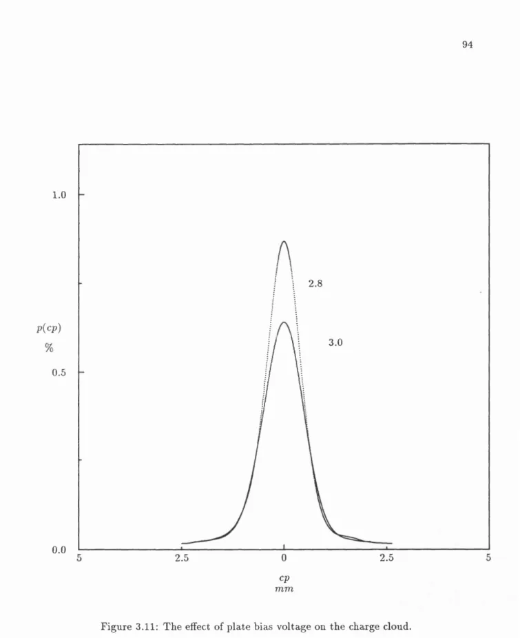
3.11 The effect of plate bias voltage on the charge cloud... 94
3.12 The p{cp) curve displayed in Figure 3.7, overlayed with its reflection about its centre... 96
3.13 Two overlayed p{cp) curves obtained with the pore bias angle aligned normal and parallel to the split... 97
3.14 The annular regions of the charge cloud corresponding to the three terms in Equation 3.5... 99
3.15 The vector between two minima x i and X2 obtained by minimizing along the vector V from two initial points, is conjugate to v... 107
3.16 Example of Powell’s method for finding the minimum by using conjugate directions... 107
3.17 The distribution of F obtained with the automatic search routine... I l l 4.1 Comparison of typical fits to a mean S curve, S{cp)... 117
4.2 Comparison of the success of fits with exponential and Gaussian central com ponents... 1 2 0 4.3 The one dimensional integrated probability density distributions obtained for g = 6 . 2 mm, Vg = 400 V, %. = 2.9 kV for both chevron bias angle/split orientations... 1 2 1 4.4 An example of a flat wing... 123
4.5 An example of severe modulation... 124
4.7 The fit parameters obtained with g = 6.2mm and the chevron bias angle
aligned parallel to the anode split... 129
4.8 The fit parameters obtained with g = 6.2mm and the chevron bias angle aligned perpendicular to the anode split... 130
4.9 The fit parameters obtained at an anode gap of 3.0 mm... 133
4.10 The output energy distribution from one single thickness MCP... 135
4.11 Energy distribution of output electrons a t various output angles for a single MCP... 135
4.12 Horizontal distance travelled by output electrons while traversing the MCP- anode gap for a simple ballistic model with various combinations of angles and output kinetic energies... 137
4.13 Horizontal distance travelled by a single electron in a given tim e due to Coulomb repulsion... 139
4.14 The PHD of the large data set showing the edges of the multiple gain intervals. 141 4.15 The variation of the size of the charge cloud with varying gain... 143
4.16 The variation of radii containing fixed fractions of the charge cloud with Eg. 145 4.17 The variation of radii containing fixed fractions of the charge cloud with approximate electron time of flight... 146
4.18 The variation of radii containing fixed fractions of the charge cloud with varying for = 3.0 mm... 147
4.19 The variation of radii containing fixed fractions of the charge cloud with varying Vcfoi g = 6.2 mm... 148
4.20 Comparison of ri for the two anode gaps versus Eg... 150
4.21 Comparison of r/ for the two anode gaps with respect to t / ... 151
4.22 The affect of the inter-plate voltage on the fit param eters... 154
4.23 The variation of r/ with gain due to the variation of the inter-plate gap voltage. 155 4.24 The ratio of the average limiting radii for both the bias angle/split orientations. 157 4.25 The difference between the two estimates for the centre channel, Acc for the 28 d ata sets... 160
5.1 Summary of the five steps necessary to transform the three ADC values into the one dimensional output... 162
5.2 An example of d ata th at haa undergone the coordinate rotation...164
5.3 Ideal, three arm spiral represented in r/<j> space... 167
5.4 A family of ideal spirals on a continuous series of planes, sectioned by the plane x = y... 167
5.5 An example of ghosting... 170
5.6 A corrected version of Figure 5.5... 171
5.7 The same as Figure 5.6 except that the LLD has been set to a higher value, as shown by the PHD in the bottom left comer... 171
5.8 Radius th at has been normalized with respect to pulse height, r„ plotted against <f>... 172
5.9 A similar diagram to Figure 5.8 except th a t it represents the subset of th a t d ata th a t has a flat PHD... 173
5.11 The same d ata as in Figure 5.10, but plotting the normalized radius against
pulse height... 175
5.12 The simulated variation of the radius of a Lissajous circle with respect to charge cloud size... 176
5.13 The gradient of r„(h '), a , as a function of ... 176
5.14 The Variation of a with anode gap voltage... 178
5.15 The variation of a with plate voltage and anode gap electric field strength. 179 5.16 As for Figure 5.9 after radius dependent correction... 181
5.17 As for Figure 5.11 after radius dependent correction... 181
5.18 As for Figure 5.9 after radius independent correction... 183
5.19 As for Figure 5.11 after radius independent correction... 183
5.20 The nonlinearity of the radius/pulse height relationship... 184
5.21 As for Figure 5.16 after use of a northeast compass mask ED, as described by Equation 5.28... 187
5.22 As for Figure 5.16 after use of a pseudo-compass mask ED, as described by Equation 5.30... 187
5.23 As for Figure 5.16 after use of a Sobel ED. The three figures show the effect of varying the threshold level... 189
5.24 Fragmentation of the spiral due to errors in spiral arm assignment... 190
5.25 Fits to the whole spiral... 193
5.26 The Hough transform ... 195
5.27 The Hough transform of the ideal spiral. Figure 5.3... 196
5.28 As for Figure 5.27, except the side histogram shows the variation of with 0 and the bottom histogram shows the distribution of p along the line 0 = 6m .196 5.29 The HT of Figure 5.16... 198
5.30 The reduced angle range for the HT determined by the r„ intensity distribution. 2 0 0 5.31 Comparison of the Sobel ED and the HT... 202
5.32 The variation of the spiral constants with anode gap voltage... 204
5.33 The variation of the spiral constants with plate voltage... 205
5.34 An example of spiral arm assignment by statistical distribution of p in Hough space... 207
5.35 An example of the results obtained with spiral arm assignment by using the statistical distribution of p... 209
5.36 <i>iag plotted against (f>\, demonstrating th at these two values define a spiral. 210 5.37 An example of pulse height related shifts in <!> and r „ ... 215
5.38 An example of positional shifts due to pulse height variation... 216
5.39 Image of an array of 50 pm pinholes demonstrating the linearity of the SPAN readout... 218
6.3 The Axed patterning produced when all the possible lattice points have been
illuminated once and only once... 224
6.4 The effects of variation in the anode design parameters on fixed patterning. 227 6.5 The effects of variation of user defined variables on fixed patterning...228
6 . 6 The variation of rum with h' for 8 bit ADCs... 231
6.7 This diagram is similar to Figure 6 . 2 except th a t all of the lattice points from all of the pulse height planes have been projected into one plane...232
6 . 8 The variation of fixed patterning with gain depression for fixed reference ADCs.234 6.9 Simulation of the variation of fixed patterning with varying levels of digiti zation for fixed reference ADCs... 235
6 . 1 0 Simulation of fixed patterning with varying levels of digitization with ratio- metric ADCs... 239
6 . 1 1 The shift of the spiral origin with pulse height in a system using ratiometric ADCs... 241
6.12 Aliasing between 1 1 fim pixels and pores on 15 fj,m centres as measured with a MIC detector... 242
6.13 Simulation of aliasing between 9fim pixels and pores on 15 fim centres. . . . 244
6.14 Simulation of aliasing between 9/zm pixels and pores on 8 /xm centres. . . . 244
6.15 An example of chicken wire distortion... 245
6.16 Simulated fixed patterning due to the interaction between 8 bit digitized inputs and the 2048 pixels. The image represents a flat field over 5% of the detector width located at the approximate centre... 247
6.17 Simulated fixed patterning with 3 random, extension bits on each of the inputs. The image was generated under the same conditions as Figure 6.16 but with 11 bit inputs, of which the 3 least significant bits are random. . . 247
7.1 The effects of adjacency on gain depression... 250
7.2 The variation of pulse current to strip current with count rate and size of illuminated area... 250
7.3 The Experimental Arrangement... 253
7.4 Mean MCP gain for each annulus, G(r)... 257
7.5 Relative mean gain versus annuli radius, G '(r)... 257
7.6 G'(r) for radii up to 1.5 mm ... 258
7.7 Normalized count rates per annulus for the curves in Figure 7.6...258
7.8 Pulse Height Distributions at selected radii... 259
7.9 The intrinsic variation of the mean gain with radial distance, G (r), from the centre of the pinhole for 3 plate voltages. The curves represent flat fields, i.e. the MCP was illuminated only by the diffuse X ray source... 264
7.10 The variation of normalized average gain with radial distance from the centre of the pinhole, C '(r), for 3 plate voltages... 265
7.11 Examples of linear regression fits for data obtained at UV fluxes of 300 and 4500 Hz for a 3.0 kV plate voltage... 267
7.13 Gradient and offset terms for linear regression fits for 4 d ata sets obtained
at UV count rates of 500 and 900 Hz with a plate voltage of 3.0 kV... 268
7.14 The variation of G '(r) and relative total event rates for three UV count rates, as measured with the ring... 270
7.15 Variation of G '(r) with relative total count rates... 272
7.16 Flat fields obtained at various stages of the experiment... 274
7.17 Details of the UV illumination of the ring... 278
7.18 The variation of the magnitude of long term LRGD with tim e...280
7.19 The d ata presented in 7.18 plotted linearly with respect to tim e...281
7.20 The PHDs acquired for various different regions approximately 1 0 0 hours after the last UV exposure of the ring... 283
7.21 Variation in gain for flat fields obtained at various chevron voltages after prolonged UV illumination of the ring... 284
7.22 Image distortions in a two dimensional image produced by long term LRGD. 286 7.23 Image distortions similar to those in Figure 7.22 after the MCP stack has been rotated by 1 2 0° with respect to the readout... 288
7.24 The equivalent circuit of the last dynode... 291
7.25 Schematic diagram and equivalent circuit of coupling by lateral capacitance between N active pores and Nq quiescent pores... 291
7.26 The variation of modal gain as a function of the inclination between the electric field the channel axis... 291
7.27 The reduction in secondary emission coefficient for reduced lead glass with progressive electron bombardment... 297
7.28 Auger spectrum of regions of reduced lead glass th a t are unexposed figure a, and th a t have undergone intense electron bombardment, figure b ... 297
7.29 Variation in the secondary emission coefficient for reduced lead glass with varying Potassium concentration in the surface layer... 297
L ist o f T ables
1 . 1 Properties of various M CPs... 2 0 1 . 2 Performance characteristics of two dimensional MCP readouts... 62
3.1 Example of the information returned by the automatic search routine. . . . 110 4.1 Summary of operating voltages and typical gains for measurements with an
anode gap of 6.2 mm... 114 4.2 Summary of operating voltages and typical gains for measurements with an
anode gap of 3.0 mm... 116 4.3 Comparison of two exponential and three exponential fits... 118 4.4 The fit parameters for the radial distribution as measured at 6.2 mm for both
anode orientations... 128 4.5 The fit parameters for the radial distribution obtained at a gap of 3.0 mm. 132 4.6 F it parameters determined for the gain intervals as indicated in Figure 4.14. 140 4.7 The ratio of the fit parameters for the two pore bias angle/anode split orien
tations and the difference between the two estimates of the centre channel. 156 7.1 Fit parameters for relative mean gain versus radius curves in Figure 7.6
parameters are the same as in Equation 7.4... 260 7.2 Total UV exposure and the intervals between the times at which the curves
Chapter 1
R e v ie w o f T w o D im en sio n a l
P h o to n C o u n tin g D e te c to r s
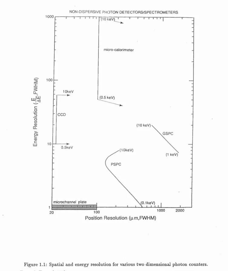
Figure 1 . 1 summarizes the performance characteristics of various two dimensional,
photon counting, X-ray detectors. Rear illuminated charge coupled devices (CCDs) can be used directly as imaging, X-ray, photon counting detector^without the need of any photon conversion or electron multiplying device. The microcalorimeter also detects an X-ray photon directly, by detecting its thermal energy in a similar manner to an infrared bolometer. At present, these detectors can only be used for photon energies greater than ~ 500 eV (Culhane, 1992 and references therein).
In the most widely used types of photon counting detectors, the incoming photon produces a t least one electron by either interacting with a gas, in gas proportional counters, or a photocathode in photomultipliers. In the later case, this photo-electron is then multi plied by a cascade of processes producing secondary electrons. If the gain is « 1 0® e“ or
larger, a current or light pulse large enough to be measured individually is produced when the secondary electrons aie collected by an anode or phosphor.
In the position sensitive gas-filled proportional counter (PSPC), electron multipli cation takes place in the gas, such as either a Xe/CH4 or A r/C H4 mixture, in the region of
NON DISPERSIVE PHOTON DETECTORS/SPECTROM ETERS 1000
micro-calorimeter
1 0 0
lOkeV
(0.5 keV) |LU
l<
CCD
(lO keV )
GSPC
O)
O.SkeV
(lOkeV)
(1 keV)
PSPC
microchannel plate to. Ik e V)
1000 2000
1 0 0
Position Resolution (p.m,FWHM)
20
photon’s energy. The cathodes are configured as either a crossed wire grid, a wire grid combined with a one dimensional, planar cathode readout such as the “backgammon” or a two dimensional, electrode readout such as the “Wedge and Strip”. These and other types of position readout are discussed below.
The gas scintillation proportional counter (GSPC), avoids the need for electron multiplication. Instead photo-electrons are created in a noble gas and pass into a region where the electric field is high enough to cause gas scintillation, producing UV photons, but the gas is not ionized. The number of photons is proportional to the number of photo electrons and therefore, incident photon energy. By omitting the electron avalanche an improvement in energy resolution of a factor ~ 2 can be achieved. Position is determined by using an array of photomultiplier tubes or a two dimensional photomultiplier (Smith & Bavdaz, 1992)
The most widely used secondary electron multiplier in image intensifiers are the discrete dynode chain photomultiplier tubes (PM Ts). Discrete dynode PMTs can produce sufficient gain. However, only mesh dynode PMTs can provide two dimensional images and the resolution is limited to approximately 300 ^m FWHM (Kume et oZ., 1986).
Since about the mid 1960s, position-sensitive photomultipliers have been used in photon counting detectors for astronomical applications. In these detectors, sometimes referred to as first generation image intensifiers, the photo-electrons from a photocathode on the input window, are accelerated by a high voltage, approximately 10 kV, and then electrostatically or magnetically focussed onto a phosphor screen (Baum, 1966). The energy gained by the electrons’ traversal of the electric field is converted to a photon pulse. If the phosphor is “sandwiched” together with another photocathode, the photon pulse will produce more photo-electrons. Each sandwich can produce an electron gain of « 100 for a
10 kV potential (Randall, 1966).
Gains of up to 10® can be obtained by cascading four such stages together, requiring 40 kV. The original Imaging Photon Counting System (IPGS), used on several ground based telescopes and as the Faint Object Camera on the Hubble Space telescope was a 4 stage tube, using a TV camera as the position readout for the optical pulses.
MicroChannel plate (MCP) based devices are similar in concept, with the four stage tube being replaced by a MCP electron multiplier. These devices are discussed in detail in the next section.
of the photo-electrons whereas the other detectors’ ultim ate resolutions are dependent on their manufacturing processes. Although gas-filled detectors only have moderate spatial resolutions, Figure 1.1, they are widely used because of their good energy resolution. The
photomultipliers offer no intrinsic energy resolution, however only the CCD has a spatial resolution comparable with the MCP. Also, only image intensifiers are sensitive to photons with energies < 1 0 0 eV and so can be used for EUV and UV/ Optical detectors as well as
X-rays.
1.1
M icroChannel P la te , S econdary E lectro n M u ltip liers
An MCP is a secondary electron multiplier consisting of an array of millions of glass tubes, called channels or pores, fused into a disk about 1 mm thick and typically
25 mm diameter. A typical MCP would have cylindrical pores with an internal diameter of 12.5 /xm. The pores are hexagonally packed with a spacing of approximately 15 fim.
Figure 1 . 2 shows a schematic representation of an MCP and Table 1 . 1 shows the wide range
of the properties of a selection of MCPs available from just one manufacturer.
Washington et al. (1971) describe the manufacturing process of MCPs. The m aterial consists basically of silica glass into which is incorporated Pb and Bi oxides which are then reduced to their metallic form by baking in a hydrogen atmosphere. This produces a high resistance surface layer. Alkali ions are also introduced into the glass to give it the required malleability and annealing temperatures. The electrical properties of metal oxide glasses have been discussed in detail by Trap (1971).
Hill (1976) has carried out Auger analysis on the surface layer of this type of bulk glass th a t has been treated in the same manner as MCPs during manufacture. Auger analysis can only examine approximately the top nanometre of a surface but by ablating the surface with an argon ion beam, the composition of the material with increasing depth could be probed. Figure 1.3 shows this element composition as a function of depth. The surface region has a high concentration of K but almost no Pb or Bi. The C is a surface contaminant and other contaminants such as S and Ca were also present. The Pb and Bi do not appear until about 1 0 to 2 0 nm below the surface. During heat treatm ent, K is
CHANNEL W ALL PRIMARY
ELECTRON
OUTPUT ELECTRONS
STRIP CURRENT
Vo
Figure 1.2: Schematic diagram of an MCP.
From Hamamatsu (1987).
Disk Diameter A (mm) 18 24.9 32.8 38.5 50 86.7 114 Electrode Diameter B (mm) 17 23.9 31.8 37.5 49 84.7 112 Effective Diam eter C (mm) 14.5 20 27 32 42 77 105 Disk Thickness D (mm) 0.48 0.80 0.4l|0.48 0.80 0.41 0.48 0.80 0.48 0.80 0.48 0.80 1.00 Channel Diam eter (jim) 12 20 10 12 20 10 12 20 12 20 12 20 25 Channel Pitch (nm) 15 25 12 15 25 12 15 25 15 25 15 25 31 Bias Angle 0 (•) 8 5 U d 8 12 8 5 .8 8 Open Area Ratio (%) 57
Electrode Material Inconel or Nl-Cr
ELECTRICAL CHARACTERISTICS
(Applied Voltage: 1000V, Vacuum: 1 x 10^ lorr (1.3 x 10^ Pa), Ambient Temperature: 25*0)
Current Gain More than 10*
Plate R esistance (MfJ) 100-1000 1 100 - 700 1 3 0 - 300 1 2 0 - 300 | 1 0 - 200 ] 1 0 -1 0 0 1 5 -5 0 Dark C urrent (A/cm') L ess than 5 x 10-"
Max. Linear Output Signal Up to 7% of the strip current *
Bi. This conducting layer is approximately 2 0 0 nm deep. The surface layer consists basically
of silica and the resistance of this layer is approximately twice th a t of the conducting layer. Figure 1.4 shows the secondary emission coefficient, S, for the reduced glass mate rial. The shape of the curve is characteristic for all materials. As primary electron energy increases, more energy is available to produce secondary electrons within the escape depth of the material. However, if the primary energy is increased too much, secondary electrons are produced much deeper in the material so th a t many do not have enough energy to escape.
Hill (1976) has calculated th at the escape depth of the reduced material is ap proximately 3.3 nm. Therefore, the secondary electrons come from the layer th a t consists mainly of silica. Also, the emissive layer is separated from the conducting layer by a high resistance region several nanometers thick.
When the interior of a channel is reduced, the channel surface behaves as a con tinuous dynode and the channel wall contains the conducting layer, through which current flows, providing electrons to the thin emissive layer at the channel surface. The conducting layer has quite high resistance so the channel wall behaves as a dynode resistance chain.
The two faces of the MCP are coated with an evaporated layer of conductor such as Nichrome or Inconel. These conductive layers serve as the input and output electrodes and connect all of the pores in parallel. The total resistance between the two electrodes is the parallel combination of the resistance for each channel and is of the order of 1 0 0 Mft.
MCPs are high gain devices which are physically small and require relatively small voltages, compared to first generation image intensifiers, and power, ^ 10 mW. These factors make them particularly well suited for space use apart from their fragility and cleanliness requirements. Spatial resolution is limited only by pore spacing, which has been realized by some readouts (see below), and as they can be used for photon counting they have good temporal resolution. As well as electrons, MCPs are sensitive to ions, UV and X-rays. Thick MCPs, ~ 5 mm, have good have good quantum efficiencies (QE) for 7-rays (Wiza, 1979),
P b .B i
I
2
O 1 2
I
ÜJ -+ -K
Molerial removed, d ep th (nm)
Figure 1.3: The variation of element composition with depth in the glass material after reduction.
From Hill (1976).
25
15
0 5
r - " . . flormat incidonco (T
10
__J_______ L
2 0 3 0
Primory electron energy (keV)
40 5 0
Figure 1.4: The variation in the yield of secondary electrons with varying primary electron energy for the glass after reduction.
theoretical studies indicate th at they could be used to focus hard X-rays with an efficiency of up to 48 % (Wilkins et al.., 1989 and Chapman et a i, 1991).
1 .1 .1 E l e c t r o n M u ltip lic a tio n in M C P s
If we take each pore in isolation it behaves in the same manner as a Channel Electron Multiplier (CEM) (Goodrich & Wiley, 1962 and Adams & Manley, 1966). How ever, this is an approximation as it has been found th a t individual pores do interact with their neighbours. In the following discussion, only isolated channels are described. The interaction between pores will be discussed in detail in Chapter 7.
When a voltage, Vd, of the order of 1 kV, is applied to the end electrodes, an
electric held, E , is established which is parallel to the pore axis. The strip current, t,, is given by
Is - VdI RcH , (1-1)
where Rch is the resistance of a single channel. When an electron collides with the channel wall, secondary electrons may be produced. These electrons follow a parabolic trajectory, dehned by their initial energy, eV, and E , and before colliding with the channel wall again, see Figure 1.2.
Electron gain is a complicated cascade of statistical processes, which produce a wide variation in the number of electrons in individual pulses. The magnitude of the gain also depends on the energy and angle of incidence of the incoming particle. It can only be properly described statistically, e.g. Lombard & M artin (1961) and Guest (1971). In the following discussion only the average behaviour will be considered.
The average time t and distance 5 between collisions for a straight channel with diameter, d, is given by
t
~ ‘^ V 2 e ^ ’
5 = , (1.3)
2 m ^ '
where we assume th at the electrons have been emitted normally from the wall with energy
Vn- The electrons will collide with the wall with an energy
Vc = E S , (1.4)
where a is the length to diameter ratio for the pore. MCPs with a = 40 are often referred to as “single thickness plates” while if a = 80 they are called “double thickness plates”
There will be n collisions along the length of the pore where
n = ^ . (1.6)
As there are a finite number of wall collisions with approximately constant separation, continuous dynode multipliers can be described as a conventional discrete dynode secondary electron multiplier (Goodrich & Wiley, 1961, Adams & Manley, 1966 and Eberhardt, 1979, 1981). This discrete separation is not seen in practice, due to the statistical nature of multiplication and the variable penetration depths of incident particles. One im portant consequence of this model is th at most of the electrons in the output pulse will originate from the same region of the channel, the last dynode.
The number of secondary electrons produced in each collision is dependent on the change in voltage and 6
S = V k K V , (1.7)
=
.
(
1-
8)
where & is a constant. Guest (1988) has determined th a t this is a good approximation of the low energy collision typical of multiplication processes.
The increase in current along a finite length, A/ of channel is given by
At = t( 6 — 1)— , (1 9 )
and the overall gain G is given by
G = ^ , (1.10)
= , ( 1.11)
where t'o and i f are the initial and final currents respectively and G is sufficiently small (Guest, 1988).
Adams & Manley (1966) and Loty (1971) have described models in which increas ing E will increase the number of electrons emitted per collision by Equation 1 . 8 but by
applied voltage increases, the gain will rise to a maximum and then reduce, even if satura tion, see Section 1.1.3, is not taken into account. However, analysis and measurements by Gear (1971) and Eberhardt (1979) show th a t the gain increases monotonicaUy with a linear relation between log G and logVj until saturation occurs, see Figure 1.5.
Equation 1 . 8 can be expressed in terms of a as
_ Vd f k
2a VK, •
(1.12)
Substituting this expression into the expression for gain. Equation 1.11, and differentiating with respect to a
Therefore, gain is at a maximum when
- ( . . . . )
Simulations and experimental measurements by Guest (1971, 1988) show th a t the gain is a maximum where the normalized voltage, W , the potential difference between two points separated by an axial distance d is
W = — , (1.15)
a
% 2 2 . (1.16)
Assuming th at Vn « 1 eV this implies k « 0.033. Substituting these values
into Equation 1.1 2, implies that the maximum gain occurs when approximately 2 electrons
are em itted per collision. Unity gain occurs when W » 1 1. Figure 1 . 6 shows the universal
gain curve for a series of channels of varying a , W and Vd derived from a simulation. The input parameters have been kept constant as a 2 KeV electron with an angle of incidence of 13°. The simulation allows for the statistical nature of the multiplication process and therefore, indicates small gains for W % 1 1. This hgure and Equation 1.14 show th a t the
most im portant parameter for describing the gain performance of a straight channel is a.
1 .1 .2 I o n F e e d b a c k
«0*1 L /0 RATIO MCPS
L / 0 RA TIO M C P S
3
450 500 GOO TOO n o *00 woo
A P P U E O V O LT A G E , V
1500
Figure 1.5: The relation between gain and Vd.
From Eberhardt (1979).
«00 V
Figure 1.6: Universal gain curve of an MCP.
desorbed from the channel wall during electron bombardment. Adams & Manley (1966) have estimated th at the number of ions produced, iV, is
N = 6rieP , (1.17)
where n* is the number of electrons in a region of width u; at a pressure p Torr.
These ions can collide with the channel walls near the channel input producing another pulse. For sealed tubes (see below) ions can hit the photocathode, poisoning it and drastically reducing the tube lifetime (Oba &: Rehak, 1981 and Norton et of., 1991). They may also produce secondary electrons from the photocathode generating another event in another channel for a MCP. In this case, there will be two events occurring within nanoseconds of each other, which will be treated as simultaneous and will produce errors in position encoding in many readouts. These extra events could result in a regenerative feedback situation, which in extreme cases could lead to the destruction of some channels. The need to avoid ion feedback limits the maximum electron gain th a t a single straight channel can supply to 10® (Wiza, 1979).
Ion feedback can be overcome in CEMs by bending or curving the tubes as the heavy ions have much longer trajectories than the secondary electrons. MCPs can also be manufactured with curved channels, a “C plate”, (Timothy, 1974). The gain expression for a curved channel is different to th at for a straight channel due to the effect of wall curvature on the electron trajectories (Adams & Manley, 1966). Whereas a is the parameter that determines the applied voltage/gain characteristics of a straight channel, the most important param eter for a curved channel is the included angle of the curve. There is a limit to the maximum included angle practicable for curved channels in MCPs which limits the gain to w 10® e~ for a C plate (Wiza, 1979)
Another widely used method is to use two or more plates with straight channels and with the pores inclined at an angle to the normal to the MCP face. Colson et al.
the first MCP to expand and so Are several pores in the bottom plate, increasing the overall gain. The inter-plate gap is discussed in Section 4.4.5. Using these configurations, gains of
1 0^ — 1 0® e~ are obtainable with straight plates.
1 .1 .3 S a t u r a t i o n
Due to the statistical nature of the gain process a pulse height distribution (PHD) is produced. At low gains, the PHD has a negative exponential shape. However, as gains increase the PHD is no longer a quasi-exponential but a pseudo-Gaussian (see Figure 1.8). This effect is known as saturation.
There are two likely processes th at can cause saturation.
1. The space charge of electrons in the channel is sufficient to drive secondaries back
into the wall before they can acquire enough energy from the electric field to produce more secondaries (Bryant & Johnstone, 1965).
2. There is a limit on the maximum rate at which electrons can be supplied through
the channel wall to the emissive layer. If more electrons are extracted than can be supplied a positive charge will build up. As the wall resistance is very high, the time constant is of the order of milliseconds while the total length of the electron pulse is of the order of 1 0 ps. Therefore, the positive charge cannot be neutralized during the
pulse (Evans, 1965).
Experiment and simulation have determined th at the dominant process in satura tion is space charge for curved channels (Adams & Manley, 1966 and Schmidt & Hendee, 1966) and wall charging for straight channels (Adams & Manley, 1966, Loty, 1979 and Guest, 1988).
Chevron MOP slack
m
E lectron clo u d footprint
Strip W edge
W e d g e an d strip
a n o d e Algorithm
p rocessin g electronics
Figure 1.7: Schematic diagram of a Chevron pair MCP configuration combined with a
Wedge and Strip Anode.
The Wedge and Strip Anode is discussed in Section 1.3.2.
1 0"
1 0' “
THREE-STAGE
1 0*
1 0’
TWOSTAGE
1 0 *
^ SINGLE-STAGE
1 0'
500 600 700 800 900 1000 1100 1200
APPLIED VOLTAGE PER STAGE ( V )
900 800 700 ^ 600 500
300
I 0 <<I 1 <<I 2
g
200 100
0 5 10 15 20 25
Distance (h Diameters) from Input
Figure 1.9: The variation of the potential within a channel with increasing saturation. The values Iq, Ii and I2 refer to increeising input current and distance along the channel is
measured in pore diameters. From Guest (1988).
2 0
I 5
f p : 3 0 0 eV n o ffnol in cid e n c e
X--- X— X--- !—^
X
X
\
1 0 j :_L j__ 10"'^ 10'
Log,Q som ple current ( / s - / p ) ( A )
Figure 1.10: The reduction of the secondary emission coefficient, <5, with surface charging for reduced lead glass.
Increasing Vd increases saturation and moves the region of unity gain further up the pore, reducing the length of pore th a t contributes effectively to gain. Eventually, the region of unity gain extends along most of the length of the channel. The region near the input then has a much larger E than in the unsaturated case and is the only region making an effective contribution to the gain.
Saturated PHDs are a problem for image intensifiera being used in the proportional mode, in which the output current is proportional to the input current. Saturation places an upper lim it on the output current and therefore output image intensity. In order to maintain proportionality, the MCPs are operated in the low gain regime with a negative exponential PHD.
In a photon-counting detector, it is only necessary to obtain one pulse per input photon. The pulse amplitude is not im portant, so long as it is above a threshold defined by the signal to noise ratio (SNR) required by the position readout. In practice, a lower level discriminator (LLD) is used to reject events lying below th a t treshold. A PHD with the largest percentage of points lying above the LLD is necessary to ensure the best photometric linearity of the detector. It can be seen from the PHDs in Figure 1 . 8 th a t the higher the
saturation, the higher the percentage of points with large amplitudes. Therefore, high saturations are desirable in photon counting detectors.
Saturated PHDs are described by two parameters, the modal gain, i.e. the gain which represents the mode of the PHD and the gain resolution or saturation, the ratio of the PHD FWHM to the modal gain.
1 .1 .4 G a in D e p r e s sio n w ith C o u n t R a te
As described above, the neutralization of the positive wall charge takes a finite time, of the order of milliseconds, due to the time constant of the channel. If another cascade occurs in the channel before the wall charge is neutralized, the electric field will be still be reduced at the bottom of the channel and this region will not make an effective contribution to the gain. This depresses the modal gain (Loty, 1971, Timothy, 1981, Neischmidt et a l,
1982, Siegmund et a l, 1985), and moves the PHD to lower values. Zombeck & Fraser, (1991) have presented PHDs for various count rates. Figure 1.1 1.
a a
-71 ct s = 5.9 X 10’
140
-1
i
1
disc, threshold0.0
OwwW I
HRI Pulse Height Spectrum
t o o vm n o courrit • * !
I
HRI Pulse Height Spectrum
to o am 77% cmwit m-1
220 ct s
500 200 too 0 tZOA 400
772 ct s
h
00
124 ct s'
« 0
-I
1
400
CKMHlf
HRI Pulse Height Spectrum
to o
443 ct s'
500
-I
tlOO ZOOO
CtaiMl I
HRI Pulse Height Spectrum
1117 MwiU i - l
1117 ct s'
n
1100
CMMkd I
Figure 1.11: PHDs exhibiting various degrees of gain depression with variation o ^ count rate.
local count rate, most of the PHD will fall below the LLD, effectively paralysing the pore. This process is the ultimate limit on the point source count rates for all MCP detectors. Most position readouts can achieve point source count rates at this limit. In MCPs with an individual channel resistance, Rcht of « 1 0^^ D, significant gain depression can occur at
count rates as low as « 1 Hz.pore"^, (Fraser et oZ., 1991b and Nartallo Garcia, 1990), see
Figure 1.12.
Note th at in the Figure 1.11 the absolute width of the PHD does not vary signifi cantly as the gain is depressed. This is also shown in the saturation graph in Figure 1.12. Saturation is a relative measurement of the PHD width with respect to the modal gain. The variation in saturation in this diagram is due in the main part to the reduction in modal gain rather than an increase in the absolute width of the PHD.
As the count rate is limited by the time constant of the pores, the photometric linearity can be increased by reducing the resistance of the pores. Evaluation of lower resistance MCPs have shown th at countrates of % 40 and 500 Hz.pore~^ are sustainable with minimal gain depression with Rch % 1 0^^ and 1 0^^ D, respectively, (Siegmund et oZ.,
1991 and Slater & Timothy, 1991).
However, Rf^ cannot be made arbitrarily small and these values represent the approximate limit for conventional, stable operation of MCPs. The resistance of the chan nels has a negative temperature coefficient and Joule heating by the strip current running through the walls will raise temperatures. Thermal runaway will occur for power densities above 0 . 1 W.cm“ ^. A 25 mm diameter plate will be unstable with a resistance less than
roughly 5 MQ. This corresponds to a limiting count rate of several times 1 0® Hz.cm"^
(Feller, 1991). Assuming th at the plate has 12.5 /im pores on 15 /im centres, there are « 5 X 10® pores.cm"^. This limiting count rate corresponds to several hundred Hz.pore”"^ for Rch « 1 0^® Ü.
In conventional MCP mounts, almost all the heat must be removed radiatively as there is poor lateral conduction through the plate edges. Feller (1991) found th a t by connecting one MCP face directly to a heat sink. Joule heating was removed far more efficiently by conduction and power dissipations of up to 3 W .cm“ ® could be maintained. This allowed the continuous, stable use of a 25 mm, 750 kft, i.e Rch % 10^® ft, plate at 1.7 kV with a maximum output rate of 1 2 k H z . p o r e " A t a voltage above 1.75 kV, the
plate once more became thermally unstable.
perfor-Modtl G «in V* count raU
U U
-I 0.7 -0.6
0.4
OJ
-0.1
-0 100 200 300 400 500
Coun(«/»«con<j 75 micfon «pot «ix*
rwHM v« Count Ra(«
Z 6
-2.6
2.4
16 -1.6
-0.8
0.4
-4 0 0 500
0 100 200 3 0 0
C o un lt/M co n d 75 micron spot *tz«
Figure 1.12: Gain depression with count rate with high resistance plates.
mance dramatically, it requires a direct connection to the MCP face. However, it is not applicable to large format, high resolution imagers as all of the current readouts th at pro duce this performance require a gap between the MCP and the readout of at least 1 0 0 /zm
and in some cases millimetres, see Section 1.3.2.
1.2
M C P B ased P h o to m u ltip liers
1 .2 .1 E U V a n d X -R a y P h o to m u ltip lie r s
The quantum efficiency (QE) of an uncoated MCP in the UV is shown in Fig ure 1.13. The QE at these and soft X ray wavelengths can be enhanced by depositing a photocathode, for example Csl or MgF2 directly onto the MCP face. The sensitivity of an
MCP can also be extended into the hard X ray region by using a 1 0 0 /im Au photocathode
mounted directly onto the front of an MCP. Detected quantum efficiencies of « 0 . 2 % have
been achieved for 1 MeV X-rays (Veaux et al., 1991).
In operation, the whole MCP stack and the readout are open to vacuum, so these detectors are often called open-window detectors. These types of detectors have flown on many X-ray/EUV satellites, e.g. Einstein, EXOSAT and ROSAT (2k>mbeck & Fraser, 1991 and references therein) and are to be used on the Extreme Ultraviolet Explorer (Sieg mund et al., 1985) &nd Solar and Heliospheric Observatory (SOHO) (Breeveld et al., 1992a) satellites.
1 .2 .2 O p t ic a l/U V P h o to m u ltip lie r s ^
For wavelengths from about 200 to 600 nm, the QE of a bare MCP falls of rapidly, so a photocathode is necessary. A typical photocathode for these wavelengths is the multi alkali S2 0, see Figure 1.14.
There are a number of practical reasons why these photocathodes are not deposited directly onto the MCP surface. The photo-electrons liberated from the microchannel plate would have relatively low energies and those created other than within the channels would probably be lost. Also, during the deposition of the photocathode it might prove impossible to prevent a slight separation of photocathode constituents. These could end up deep inside the pores which could lead to “switched on channels” .
transpar-100
-Csl COATED MCP
8 10 12 14
WAVELENGTH (nm )
too
• C il 3 5 0 0 A oC»l wool " B or, MCP
2
o
6 0 0 1000 1400 1800 2000 2 400
200
X(A)
Figure 1.13: UV Quantum Efficiency of MCP material.
The left diagram is from Hamamatsu (1987) and the right figure is from Samson (1984).
Wavelength (nm)
ent material, e.g. MgFg, Sapphire or quartz, see Figure 1.15. An electric field is applied to the gap between the photocathode and the MCP, accelerating the photo-electrons towards the MCP. This process is known as proximity focussing.
The photo-electrons have a Maxwellian distribution in transverse velocities which produces a distribution of points at which the electrons are incident on the surface of the MCP. This represents the ultim ate limit of resolution in a sealed tube intensifier. The point spread function (PSF) of this distribution is given by Eberhardt (1977) as
P ( r) = , (1.18)
where P (0) is the peak of the PSF, r is the distance from the peak, V is the voltage applied across the gap of width L and is the mean radial emission energy of the photo-electrons. As wavelength decreases, Vr increases and so the FWHM of the PSF increases. The FWHM of the PSF can be determined from this equation as
F W H M = 3.33L{Vr/V)i , (1.19)
(Lyons, 1985).
In practice, the proximity gap is kept as small as possible and V is as large as possible to improve resolution. Figure 1.16 shows theoretical PSF FWHM curves for two gaps and various voltages over a wavelength range of 400 to 600 nm, using Vr measurements for a multi-alkali photocathode from Eberhardt (1977). The PSF for UV radiation would be higher but to date, no Vr measurements for these wavelengths have been presented in the literature. The maximum electric field strength will depend on the design of the intensifier, however, Lyons (1985) states th a t a maximum field strength from 1.5 to 2 kV.mm""^ is
reasonable. A proximity gap of 300 /xm is the limit available in most commercial devices but a gap of 150 //m has been reported (Clampin et a l, 1988). Figure 1.16 shows th a t for a 300 fjLm gap, the PSF FWHM will be approximately 2 0 fim for all voltages. This wiU be
value assumed for the PSF for the rest of this chapter.
Vacuums of the order of 1 0” ^® torr are required to avoid poisoning of the pho
Figure 1.15: Schematic diagram of a sealed tube.
150
100
S X
£
I
£
50
300
100 200 300 400 50 0 600 7 0 0 800 P r o x im ity F o c u sin g V o ltag e (V olts) 900
Figure 1.16: Proximity focussing PSF FWHM.
1.3
M C P P osition R ead o u ts
MCP baaed detectors can be divided into two m ajor types.
1. Light amplification detectors, in which the electron cloud produced by the MCP is
incident upon a phosphor producing a large pulse of photons which are optically coupled to the detector, usually a CCD.
2. Charge measurement detectors, in which the centroid of the charge cloud is directly measured by a series of electrodes. The positional readouts used in these detectors
tn
can be used MCP and gas proportional detectors.
A
1 .3 .1 L ig h t A m p lific a tio n D e te c to r s
There are two basic types of Light Amplification Detectors.
1. Direct Readout Detectors.
In direct readout detectors, the position of the intensified events is immediately read out and the detector performs no integration of events, e.g. PAPA.
2. Scanned Readout Detectors.
In scanned readout detectors the event is captured and stored by a detector and read out later when the whole or part of the detector is scanned. Examples of this type of detector are the vidicon camera, the Self-scanned PhotoDiode array (SPD) and the Charge Coupled Device (CCD).
P A P A
a set of progressively finer Gray coded masks, with the spatial frequency of the finest mask determining pixel size.
It is possible, using a set of 9 photomultipliers and their respective masks to determine the photon event position in the x direction to one of 512 positions. A similar arrangement is implemented in the y direction using another 9 photomultiplier tubes and a set of masks mounted orthogonally to the original set.
Using all 19 outputs from the above photomultipliers an 18 bit (z, y) address can be generated which represents the arrival position of each detected photon. Therefore, 19 amplifier channels each consisting of a preamp and a discriminator are required.
At present, PAPA can provide up to 512 x 512 pixels, although formats of up to 4000 X 4000 pixels have been proposed (Papaliolios et oZ., 1985). PAPAs have been built
with 25 mm active diameters (Norton, 1990). Assuming an 18 X 18 mm square, 512 pixels,
20 fim defocussing in the proximity gap and a pore spacing of 15 /xm, the resolution will be approximately equal to the quadratic sum of these components, i.e.
PSF FWHM = V3 5 2 + 202 ^ 1 5 2 ^ (1.20)
« 44 fim . (1.21)
The MCP charge cloud is incident on a P47 phosphor which has an extremely short decay time of 2 0 0 ns. This implies a deadtime of 1 fjis per event (Norton, 1990).
In a paralysable detector, a subsequent event arriving within the initial event’s deadtime, will extend the nonreceptive period of the detector by a further deadtime. In PAPA an other event occurring during the phosphor decay time will lead to a wrong address being returned. The detector will not return a correct address for a third event, until after the deadtime associated with the second event has expired. PAPA can therefore be described as a paralysable detector. Given the relation for a paralysable detector (Lampton & Bixler, 1985),
R ' = Re~’^'’ , (1.22)
where R is the mean rate at the input, R ' is the mean rate at the output and r is the deadtime, then there will be a 1 0% counting loss at a random arrival rate of 1 0® Hz. The
maximum point count rate for PAPA will be ultimately set by the channel recovery time of the MCP.
THERM OELECTRIC COOLER /
LENS m a s k s
ARRAY
^
t
INCOMING PH O TO N
COLLIMATOR
/
FIELD L E N S E S
__________
Q [) C h a n n e l 0
0 D
C h a n n el 2EB
ED 0 I) stro b e
I I 0 ^ C h a n n el 3
A / D
EO
0 D C hannel 1
t
FIELD
FLATTENING L E N S E S
P M T s
BINARY CODE GRAY CODE
X-POSITION
MASKS
MASKS
DATA CHANNEL
NO
NO
0
YES
YES
YES
NO
DETECTED AND INTENSIFIED PHOTON
Figure 1.17: Schematic diagram of the PAPA detector.
the reduced mean rate is given by
(Lampton & Bixler, 1985). In this case, a random arrival rate of 10^ Hz, will also cause a 10 % counting loss. All count rates quoted in this work correspond to this level of counting loss.
The PAPA detector requires th at the mechanical alignment of the optics system with the coded masks be extremely precise. Sub-micron shifts in the mask position intro duces serious fixed patterning noise in the final output image (Norton, 1990), i.e. some pixels detect higher intensities than others under constant illumination.
Scanned R eadout D etectors
The vidicon (generic name) has a dense array of reverse biased diodes on a silicon substrate. An incident photon is converted into electron-hole pairs which locally discharge the diodes. The wafer is then raster scanned with an electron beam and the current required to recharge each diode reflects the intensity at th a t point. Vidicons are slow devices, intense signals can spill over into the next diode and more than one scan of the electron beam may be required to readout intense signals (Richter & Ho, 1986).
A SPD consists of an array of photodiodes connected to an output signal line via switches. A shift register sequentially recharges each diode which effectively measures the stored signal. The CCD stores signal in a similar way. The charge is transported by an analog shift register. The SPD and CCD have very similar operational characteristics. However, the CCD does have some advantages over the SPD, it is easier to construct two dimensional CCDs and the CCD’s lower output capacitance means it can be clocked faster and have lower noise (Richter & Ho, 1986). The CCD is therefore the detector used in most modern scanned readout systems.
CC D B ased D etectors
In CCD based detectors the pulse of photons is optically coupled to one or more CCDs through a fibre-optic bundle. The small areaa of CCDs 1 cm^ compared to MCPs can be