334 |
P a g e
SOFT ERROR TOLERANT HIGHLY RELIABLE
MULTIPORT MEMORY CELL DESIGN
Murugeswaran S
1, Shiymala S
21
PG Scholar,
2Professor, Department of VLSI Design, SBM College of Technology, Dindugal,
Tamilnadu, (India).
ABSTRACT
In a Very Large Scale Integrated (VLSI) circuit, memory design and development is the predominant domain. Static
Random Access Memory (SRAM) is used as a discrete component in earlier stages of the system design, and now it
is used as an Embedded SRAM for System on Chip (SOC) designs. Designing and developing of memory in each
manufacturing technology node is continuous challenge and it is the first priority of the evaluation of manufacturing
technology. Reliability of a product describes the ability of a system or component to perform its required functions
under stated conditions for a specific period of time. Quality of product is decided based on reliability of the chip.
For an Integrated Circuit (IC), as a critical product specification under today’s aggressive technology scaling, to
achieve reliability in leading-edge technology has always been very difficult and costly to measure. In this project,
highly reliable multiport SRAM memory cell for CMOS technology is designed and developed. Simulation results
are reported to show that the proposed two port memory cell (14T) is highly reliable for Single Event Upset (SEU).
Single soft error is modelled for evaluating the multiport memory cell which is self-tolerant with respect to SEU
Keywords: SRAM, Multi Port Memory, Single Event Upset (SEU), CMOS, Soft Error, Reliability, Read
– Write Circuitry, Power Delay Product (PDP)
I INTRODUCTION
Single Event Upsets (SEUs) induced by particle radiation are becoming an increasing important threat to the
reliability of memories fabricated in Nano scale CMOS technologies. SEUs are caused by particle-induced charge
which is derived from direct ionization from heavy ions and indirect ionization from protons and neutrons. An
energetic particle passes through the sensitive node of a semiconductor device it frees electron-hole pairs along its
path as it loses energy. The electric field present in a reverse-biased junction depletion region can separate
electron-hole pairs, so that the particle- induced charge is very efficiently collected through drift processes leading to an
accumulation of extra charge at the sensitive node. When the amplitude of the accumulated charge is enough and the
time is long enough, it can generate a large voltage transient pulse which changes temporarily the value of the
sensitive node. In addition, the sensitive areas of semiconductor device are the strongly reverse biased diffusion
areas where the induced transient current flows from the N-type diffusion to the P-type diffusion. As a result, when a
radiation particle strikes PMOS transistor, only a positive transient pulse is generated, on the contrary, when a
335 |
P a g e
II SRAM DESIGN
The demand for static random-access memory (SRAM) is increasing with large use of SRAM in System-On-Chip
and high performance VLSI circuits. Due to the need of battery operated device, the scaling in CMOS technology
continues. Nanoscale CMOS SRAM memory design faces several challenges like reducing noise margins and
increasing variability, due to the continuous technology scaling. In SRAM the data is lost when the memory is not
electrically powered. Advances in chip design using CMOS technology have made possible the design of chips for
higher integration, faster performance, and lower power consumption. To achieve these objectives, the feature size
of CMOS devices has been dramatically scaled to smaller dimensions over the last few years. Power consumption of
SRAMs account for a significant portion of the overall chip power consumption and due to high density, low power
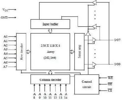
operation is a feature that has become a necessity in today‘s microprocessors. The basic architecture of a static RAM
includes one or more rectangular arrays of memory cells with support circuitry to decode addresses, and implement
the required read and write operations. Additional support circuitry used to implement special features, such as burst
operation, may also be present on the chip
Fig 2.1 SRAM Block diagram
2.1 Conventional 6T SRAM Cell
An SRAM memory cell is a bi-stable flip-flop made up of four to six transistors. The flip-flop may be in either of
two states that can be interpreted by the support circuitry to be a 1 or a 0. A typical SRAM cell is made up of six
MOSFETs. Each bit in an SRAM is stored on four transistors (M1, M2, M3, M4) that form two cross-coupled
inverters. This storage cell has two stable states which are used to denote 0 and 1. Two additional access transistors
serve to control the access to a storage cell during read and write operations. In addition to such six-transistor (6T)
SRAM, other kinds of SRAM chips use 4, 8, 10 (4T, 8T, 10T SRAM), or more transistors per bit. Four-transistor
SRAM is quite common in stand-alone SRAM devices (as opposed to SRAM used for CPU caches), implemented in
336 |
P a g e
The principal drawback of using 4T SRAM is increased static power due to the constant current flow through one ofthe pull-down transistors. This is sometimes used to implement more than one (read and/or write) port, which may
be useful in certain types of video memory and register files implemented with multi-ported SRAM circuitry.
Generally, the fewer transistors needed per cell, the smaller each cell can be. Since the cost of processing silicon
wafer is relatively fixed, using smaller cells. Access to the cell is enabled by the word line (WL in figure) which
controls the two access transistors M5 and M6 which, in turn, control whether the cell should be connected to the bit
lines: BL and BL bar. They are used to transfer data for both read and write operations. Although it is not strictly
necessary to have two bit lines, both the signal and its inverse are typically provided in order to improve noise
margins.
Fig.2.2 Conventional 6T SRAM cell
2.2 Read and Write Operations
To select a cell, the two access transistors must be ―on‖ so the elementary cell (the flip-flop) can be connected to the
internal SRAM circuitry. These two access transistors of a cell are connected to the word line (also called row or X
address). The selected row will be set at VCC. The two flip-flop sides are thus connected to a pair of lines, B and B.
The bit lines are also called columns or Y addresses. During a read operation these two bit lines are connected to the
sense amplifier that recognizes if a logic data ―1‖ or ―0‖ is stored in the selected elementary cell. This sense
amplifier then transfers the logic state to the output buffer which is connected to the output pad. There are as many
sense amplifiers as there are output pads. During a write operation, data comes from the input pad. It then moves to
the write circuitry. Since the write circuitry drivers are stronger than the cell flip-flop transistors, the data will be
forced onto the cell. When the read/write operation is completed, the word line (row) is set to 0V, the cell (flip-flop)
337 |
P a g e
Fig2.3 Read Write Operation of SRAM
2.3 Problems in 6T SRAM Cell
The potential stability problem of this design arises during read and writes operation, where the cell is most
vulnerable towards noise and thus the stability of the cell is affected. If the cell structure is not designed properly, it
may change its state during read and write operation. There are two types of noise margin which affects the Cell
stability that are discussed shortly.
During the read operation, a stored ―0‖ can be overwritten by a ―1‖ when the voltage at node V1 reaches the Vth of nMOS N1 to pull node V2 down to ―0‖ and in turn pull node V1 up even further to ―1‖ due to the mechanism of
positive feedback. This results in wrong data being read or a destructive read when the cell changes
state.Conventional 6T SRAM suffers severe stability degradation due to access disturbance at low–power mode.
2.4 8T SRAM Cell
With the aggressive scaling in technology, substantial problems have been encountered when the conventional 6T
(six transistors) SRAM cell configuration is utilized. This cell shows poor stability at very small feature sizes, the
hold and read static noise margins are small for robust operation. Therefore, an extensive literature can be found on
designing SRAM cells for low power operation in the deep sub-micron/nano ranges. The common approach to meet
the objective of low power design is to add more transistors to the original 6T cell. An 8T cell can be found to solve
338 |
P a g e
through M6) is identical to a conventional 6T SRAM cell. Two additional transistors M7 and M8 (thus yielding an8T cell design) are employed in to reduce the leakage current.
Fig 2.3 8T SRAM Circuit
2.5 Read and Write Operations
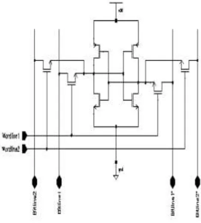
This Circuit is two write-read(2WR) type of 8T-SRAMmemory cell which has similar structure with the standard
single-port SRAM. But it has two sets of data and address paths. So this is a dual-port memory cell. Each address
and data path can complete the write and read operation independently. This SRAM cell is the component to store
binary information. It has both read and write capabilities. The word line defines operational modes.
When both Wordline1=Wordline2=0, both access transistors are off and cell is isolated. To perform read
operation.
When Worldline1=1 and Worldline2=0, the Bitline1 is selected and perform the write operation.
When Worldline1=0 and Worldline2=1, the Bitline2 is selected and perform the write operation.
When Worldline1=1 and Worldline2=1, the output is ―AND‖ operation of Bitline1 and Bitline2.
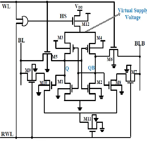
2.6 12T SRAM Cell
The proposed SRAM cell is demonstrated in figure 2.4.This structureconsists of 12 transistors which six main
transistors are same as conventional 6T. The four additional transistors respect with 6T are used to separating the
read and write path of cell. The cell is single ended structure which does the read operation from one side of cell.
Using separated path for read and write operation increases the control over the array of the cell in the catch design
by simultaneous read and write operations which is in contrast with shared access path as conventional 6T cell.
339 |
P a g e
Signal (HS) is produced by them. Both write and read modes are called active mode. For choosing between activeand idle (hold) mode, M12 transistor is used on the top place which separates virtual supply voltage from supply
voltage rail. This transistor acts as a power gating transistor. In active mode the M12 transistor should be in ON
mode by producing zero in HS signal (HS=0). After that the write and read operation can be done.
Fig 2.412T SRAM Circuit
2.6 Read and Write Operations
The write paths proposed architecture consist of two transistors (M5 and M6). In write mode, these
transistors activate with WWL signal and write the value of BL and BLB on the storage nodes. The write
operation can be performed at supply voltages as lower voltage. Inability of access transistors to change
the cell‘s value in write operation is called write failure.The read operation is done only from QB storage
node. In this mode RWL signal becomes one and BL and BBL pre-charge to one. When cell saves the
one, (Q=1 and QB=0) the M10 becomes ON and reads the Q node by passing the current through M8 and
M9. On the other case, when zero is saved in cell (Q=0 and QB=1) the M8 becomes ON and BLB line
discharges thorough M7 and M11.
2.7 Single Event Upset
Single Event Upsets (SEU) occurs when the SEE leads to a logic gate switch, voltage transients, or alteration of
340 |
P a g e
semiconductor devices. The passing of an ionizing particle through a semiconductor device generates electron-holepairs (EHPs) along the track path and may be collected at the terminals of a device. Linear Energy Transfer (LET) is
defined as the energy loss per unit path length, normalized by the density of the material. LET has units of
MeV/mg/cm2. A calculation of the charge deposited per unit length can be determined if the LET of the ion, average
energy needed to create an EHP for a material, and density of the material are known .For silicon, an ion with a LET
of 97 MeV/mg/cm2 will deposit 1pC of charge per micron length of the ion track.SEUs don‘t just happen in deep
space or when high levels of radiation are present. The same cosmic rays that warm the earth's atmosphere carry
energetic particles that cause upsets in earth-based equipment.
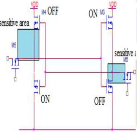
III SENSITIVE NODES
In CMOS circuits, the ―off‖ transistors struck by a heavy ion in the junction area are most sensitive to single event
upset (SEU) by particles with high enough LET (linear energy transfer) of around 20 MeV-cm2/mg. When these
particles hit the silicon bulk, the minority carriers are created and if collected by the source drain diffusion regions,
the change of the voltage value of those nodes occurs. The induced transient voltage pulse may propagate through
several of logic gates. Because a particle can induce an SEU when it strikes either the channel region of an off
NMOS transistor or the drain region of an off PMOS transistor, it is considered that the strike at an off PMOS drain
area. Particles can induce SEU when it strikes at the channel region of an off NMOS transistor or the drain region of
an off PMOS transistor. The ionization can induce a current pulse in a p-n junction. A schematic view of how the
SEE induced current pulse translates into an SEE induced voltage pulse is shown in figure 3.1. Single event upsets
are events in which an incident particle can strike key node within a device resulting in a local ionization that can
cause a state change in a bit with sufficient voltage.
341 |
P a g e
When a PMOS is struck, a positive transient pulse in induced which is 0 to 1 SEU and when NMOS is struck anegative transient pulse is generated which is 1 to 0 SEU.
Fig 3.2 0 to 1 SEU and 1 to 0 SEU
A particle can induce SEU when it strikes at the channel region of an off NMOS transistor or the drain region of an
off PMOS transistor. The ionization can induce a current pulse in a p-n junction.
Fig 3.3 1 to 0 SEU occurrence in SRAM 6T cell
Using radiation hardened memory cells to increase the SEU immunity is a less area, power and
delay consuming solution.
IV PROPOSED METHOD
In order to cope with the different drawbacks a new low-power and highly reliable radiation hardened memory cell
is proposed using 12 transistors, which is capable of fully tolerating SEU at its any sensitive node, but also can
tolerate multiple-node upset on two fixed nodes independent of the stored value. Here, access transistors are NMOS
342 |
P a g e
which are connected to bit lines BL and BLN through access transistors N8 and N1 respectively.First, Holdoperation is considered. Word line WL is ‗0‘, transistors P3, P4, N5, N6 and N4 are turned ON and the other
transistors are turned OFF. It is shown that the state of the memory cell is maintained. Second, Read operation is
introduced. Bit lines BL and BLN are pre-charged to VDD. When word line WL is ‗1‘, node Q keeps its initial state
‗1‘, because transistors P3, P4 and N5 are still ON. However, bit line BLN is discharged through transistors N1 and
N4. Then according to the voltage difference between bit lines BL and BLN, the state of the memory cell is output
by a differential sense amplifier
.
Fig 4.1 Radiation Hardened Memory Cell – 12T
343 |
P a g e
Finally, in order to modify the state of this cell, word line WL is ‗1‘, and bit lines BL and BLN are set to ‗0‘ and ‗1‘respectively. Node QN is forced to ‗1‘, thus transistors N7, N3, P1 and N2 are turned ON, transistors P3, P4 and N5
are turned OFF. Simultaneously node Q is pulled down to ‗0‘ so that transistors N4 and N6 are both OFF and
transistor P2 is ON. Then word line WL ischanged to ‗0‘, the new state of the memory cell isstored.
Fig 4.3 14T Radiation Hardened Memory Cell
344 |
P a g e
SRAM circuits are designed for both read and write operation also with and without SEU for 6T, 8T, 12T and 14Ttechniques. From Results we analyzed that 12T and 14T SRAM circuits are not affected even if the SEU are injected
and retain the data and are proved reliable circuits. Also analysis have shown that 14T SRAM transistor consume
very less power when compared to other circuits. But when there is a SEU and when the data reliability is
maintained 14T SRAM consumes more power and very less delay.
Table: 4.1 Comparison of Power, Delay and PDP for SRAM circuits.
Circuit Model
RESULTS
DELAY POWER PDP
6T SRAM_WR 39ns 251uw 10pJ
6T SRAM_SEU 9.9ns 2.71Mw 2.71mJ
8T SRAM_WR 29ns 241uw 7.2pJ
8T SRAM_SEU_RD 29ns 1.68Pw 50.6MJ
12T SRAM_WR 40ns 232uw 9.3pJ
12TSRAM_SEU_RD 39ps 6.6Gw 26.7MJ
14T SRAM_WR 29ns 124uw 3.73pJ
14T SRAM_SEU 41ps 48.7Gw 19J
345 |
P a g e
Table 4.1 shows that when there is a SEU, the proposed 12T and 14T hardened memory cells consume higher powerwith reduced delay which is shown in the comparison chart.
V CONCLUSION
In this paper, a novel low-power and highly reliable radiation hardened memory cell RHM-12T and RHM 14-T
structures are proposed to provide perfect protection against SEU in memory. Reliability of a product describes the
ability of a system or component to perform its required functions under stated conditions for a specified period of
time. Quality of product is decided based on reliability of the chip. For an Integrated Circuit (IC), as a critical
product specification under today‘s aggressive technology scaling, reliability has always been very difficult and
costly to measure, and to achieve in leading-edge technology. In this project design and development of SRAM
circuits with various methods of implementation carried out with different transistor count with 6T, 8T, 12T and 14T
logics with and without Single Event Upset. From the results, it is proved that 12T and 14T transistors are reliable
and retain the data even at presence of SEU whereas other two logic undergoes SEU error. Therefore, designers
should choose the optimal sizes of transistors to provide a good tradeoff in terms of static noise margin and other
performances. Also power consumption is very less for 14T structure when compared to other logics. The future
enhancement can be extended to work on the power consumed by this 14T structure during the SEU event
occurrence which consumes higher power but with promising decrease in delay parameter. The future work can be
done with the SRAM logic implementation on Multi Port Memories.
REFERENCES
1. Dodd, P.E. and Massengill, L.W. ―Basic mechanisms and modeling of single-event upset in digital
microelectronics,‖ IEEE Trans. Nucl. Sci.,vol. 50, no. 3, pp. 583–602, Jun. 2003.
2. Guo, J. et al., ―Novel mixed codes for multiple-cell upsets mitigationin static RAMs,‖ IEEE Micro, vol. 33,
no. 6, pp. 66–74, Nov. 2013.
3. Hughes, H.L and Benedetto, J.M ―Radiation effects and hardening of MOS technology devices and circuits,‖
IEEE Trans. Nucl. Sci., vol. 50, no. 3, pp. 500–521, Jun. 2003.
4. Ibe, E et al., ―Impact of scaling on neutron induced soft error in SRAMsfrom an 250 nm to a 22 nm design
rule,‖ IEEE Trans. Electron Devices, vol. 57, no. 7, pp. 1527–1538, Jul. 2010.
5. Jahinuzzaman, S. M., Rennie, D. J. and Sachdev, M. ―A soft error tolerant10T SRAMbit-cellwith
differential read capability,‖ IEEE Trans.Nucl. Sci., vol. 56, no. 6, pp. 3768–3773, Dec. 2009.
6. Jung, L.S , Kim, Y.B. and Lombardi, F. ―A novel sort error hardened10T SRAM cells for low voltage
operation,‖ in Proc. MWSCAS, 2012,pp. 714–717.
7. Karnik, T. , Hazucha, P. and Patel, J. ―Characterization of soft errorscaused by single event upsets in CMOS
processes,‖ IEEE Trans. Depend.Secure Comput., vol. 1, no. 2, pp. 128–143, Apr.-Jun. 2004.
8. Liu, S. et al., ―Comparison of the susceptibility to soft errors of SRAMbased FPGA error correction codes
346 |
P a g e
9. Nan, H. and Choi, K. ―High performance, low cost, and robust soft errortolerant latch designs for nano-scale
CMOS technology,‖ IEEE Trans.Circuits Syst.—I: Reg. Papers, vol. 59, no. 7, pp. 1445–1457, Jul. 2012.
10. Nicolaidis, M. Perez, R. and Alexandrescu, D. ―Low-cost highly-robusthardened cells using blocking
feedback transistors,‖ in Proc. VTS,2008, pp. 371–376.
BIOGRAPHICAL NOTES
Mr. MURUGESWARAN S is presently pursuing M.E final year in Electronics and Communication Engineering
Department (specialization in VLSI design) from SBM College of Engineering and Technology, Dindugal,
Tamilnadu, India.He also holds M.S degree (Specialization in VLSI-CAD) from Manipal University.He completed
his Bachelor of Engineering (ECE) from Manonmaniam Sundaranar University, Tamilnadu in the year 1999.He also
holds two US Patents.
Dr. SHIYAMALA S, M.E., Ph.D., is working as a Professor in Electronics and Communication Engineering
Department, from SBM College of Engineering and Technology, Dindugal, Tamilnadu, India.She completed her