INTRODUCTION
GENERAL
1-3ORGANIZATION
1-4TOOLS AND ACCESSORIES. . .
1-5SYSTEM OVERVIEW
INTRODUCTION. . .
2-3SYSTEM MODULE. . .
2-5Motherboard 2-9
CPU and DMA Circuitry. . . . . . . . . . . . . . . . . . . . . . . . . . 2-15 Memory. . . . . . . . . . . . . . . . . . . . . . . . . . . . . . . . . . . . . . . 2-16 Input/Output Peripheral Interfaces 2-18
Input/Output Connectors 2-22
Motherboard Component Layout. . . . . . . . . . . . . . . . . . . . 2-25
Display Controllers 2-27
Bus Converter 2-31
Input/Output (I/O) Expansion Bus
DISPLAY ENHANCEMENT BOARD
(OPTIONAL). . . .. . . . .. . .
2-49SMALL EXPANSION BOX
(OPTIONAL). . .
2-51DISPLAY
2-52Monochrome Display . . . . . . . . . . . . . . . . . . . . . . . . . . . . . . . 2-52
Color Display (Optional) 2-54
KEYBOARD
2-56DISPLAY AND KEYBOARD EXTENSION
CABLES
2-58MINIMUM SYSTEM
CONFIGURATION
2-59EXPANDED SYSTEM
CONFIGURATION
2-60INSTALLATIONS
PHYSICAL CHARACTERISTICS. . .
3-6UNPACKING... ..
3-7OPTION INSTALLATION
3-8Removing System Module Covers. . . 3-9 Removing Upper Cover. . . 3-10 Removing Lower Cover. . . 3-11 Upgrading Motherboard Memory to 256KB or
640KB 3-12
Installing Memory Expansion Board 3-21 Upgrading Memory Expansion Board Memory to
384KB 3-27
Installing 8087 Numeric Data Processor 3-36 Replacing Mini-Floppy Disk Unit With Hard Disk
Unit. . . 3-42
Removing Upper MFD Unit 3-42
Installing 10- or 20-MB Hard Disk Units 3-46 Installing Hard Disk Controller Board . . . 3-48 Setting DIP Switches and Jumpers. . . 3-52 Installing Small Expansion Box. . . 3-63 Installing the Display Enhancement Board. . . 3-77 Installing DEB Software . . . 3-90 Floppy Disk Systems. . . 3-91 Hard Disk Systems . . . 3-94 Troubleshooting the DEB Installation. . . 3-97
Installing the Mouse 3-100
Installing New ROM Chip. . . . . . . . . . . . . . . . . . . . . . . . . 3-105 Installing the Mouse Software. . . . . . . . . . . . . . . . . . . . . . . . 3-107
Installing the Mouse Software With the Dual Diskette
Computer 3-107
Installing Mouse Software With the Hard Disk
Computer ... . . . . . . . . . . . . . . . . . . . . . . . . . . . . . . . . . . 3-109
SYSTEM INSTALLATION. . .
3-110APPLYING POWER TO THE
SYSTEM . . .
3-115DIAGNOSTICS
INTRODUCTION. . .
4-5RESIDENT DIAGNOSTICS. . .
4-7 Operating Procedures. . . . . . . . . . . . . . . . . . . . . . . . . . . . . . . 4-8 Test Descriptions. . . . . . . . . . . . . . . . . . . . . . . . . . . . . . . . . . 4-10Error Messages. . . . . . . . . . . . . . . . . . . . . . . . . . . . . . . . . 4-15
CUSTOMER TEST
DIAGNOSTICS
4-20Loading Customer Test 4-21
Operating Procedures. . . . . . . . . . . . . . . . . . . . . . . . . . . . . . . 4-22 Automatic Mode . . . . . . . . . . . . . . . . . . . . . . . . . . . . . . . . 4-23
Memory Test. . . 4-33 Keyboard Test. . . 4-34
Video System Test 4-35
Parallel Port Test . . . 4-36
Serial Port( s) Test 4-37
48 TPI Floppy Disk Test . . . 4-37 HDU Drive and Controller Test 4-38 Parallel Printer Test. . . 4-39
8087 Math Co-Processor 4-41
Mouse Test . . . 4-41 8530 Test. . . 4-42 Video Option Board Test (DEB [Display Enhancement
Board]) . . . 4-42 2nd HDU Drive and Controller Test . . . 4-45
SYSTEM TEST DIAGNOSTICS. . .
4-47 Loading System Test . . . 4-47 Operating Procedures. . . 4-48 Test Descriptions . . . 4-58 Motherboard Test . . . 4-58 Memory Test. . . 4-60 Keyboard Test. . . 4-62Video System Test 4-63
Parallel Port Test . . . 4-67 Serial Port(s) Test (Using 8250) 4-69 48 TPI Floppy Disk Test . . . 4-71 MB HDU Drive and Controller Test. . . 4-74
8087 Math Co-Processor 4-77
Parallel Printer Test. . . 4-77 Mouse Test. . . 4-79 8530 Test. . . 4-80 Video Option Board Test [Display Enhancement Board
(DEB)] 4-80
Loading System Test (Overlay Version) . . . 4-87
STAND-ALONE MOTHERBOARD DMA
TEST DIAGNOSTICS
4-89DMA Test 4-89
STAND-ALONE LOW-LEVEL FORMAT
UTILITY TEST. . .
4-92General Characteristics 4-93
The Bad Track Table. . . 4-95 List of Operations. . . 4-96 Help. . . 4-101 HDU Configuration. . . 4-102 Low-Level Format. . . 4-105 Display and Edit Bad Track Table 4-110 Format Bad Tracks. . . 4-119 Verify Surface Test. . . 4-121
Ship the Unit 4-124
Exit Low-Level Format (LLF) Utility. . . 4-125
CUSTOMER AND SYSTEM TEST ERROR
MESSAGES. . .
4-127 100-Motherboard Tests. . . 4-127300-Memory Tests 4-129
400-Keyboard Tests . . . 4-133
500- Video Tests 4-137
600-Parallel Port Tests 4-144
700-8250 Serial Port Tests . . . 4-145 800-MFD Unit Tests. . . 4-147
20XX-Mouse Tests. . . 4-153
21XX-8530 Serial Port Tests 4-154
23XX- Video Option Board (DEB) Tests 4-155 24XX-HDU Drive No.2 Tests. . . 4-167
5
MAINTENANCE
GENERAL 5-5
Troubleshooting. . . 5-5 Replacing Faulty Modules . . . 5-5 Reminders . . . 5-6
TROUBLESHOOTING WITHOUT SYSTEM
TEST... 5-7 System Will Not Power Up Normally. . . 5-7 System Load Check on Power Supply. . . 5-9 Short Isolation Procedure. . . 5-19
Display Check 5-26
Mini-Floppy Disk Unit Check. . . 5-28 Two Mini-Floppy Disk Units. . . 5-28 One MFD Unit and One HDU . . . .. . . 5-33 System Will Not Access Hard Disk. . . 5-36
Placing Low-Level Format and Bad Track Mapping on the
Hard Disk 5-41
Partition Hard Disk for MS-DOS . . . 5-45
Formatting the Hard Disk 5-47
Hard Disk Unit "Not Ready" on Cold Start. . . 5-50 Resident Diagnostic Error Messages 5-51
TROUBLESHOOTING WITH SYSTEM
TEST... 5-54
Motherboard 5-55
Random Access Memory (RAM). . . 5-59 Determining Faulty RAM Chips. . . 5-65 Keyboard . . . 5-69 Video System. . . 5-73
Parallel Port 5-88
Serial Port Test (Using 8250) . . . 5-91 Mini-Floppy Disk Drive. . . 5-94 Hard Disk Unit . . . 5-99 Parallel Printer Test . . . 5-105
8087-2 Math Co-Processor 5-109
Mouse 5-112
Mouse Test. . . 5-114 8530 Serial Port Test . . . 5-118 Video Option Board (Display Enhancement
Board) . . . 5-121 Video Option Board Test . . . 5-125
Test Description. . . 5-142 Loading DMA Test. . . 5-142 Operating Procedures . . . 5-143
POWER SUPPLY
ADJUSTMENT . . .
5-145REPLACING FAULTY
MODULES. . .
5-148 Removing Upper Systenl Module Cover 5-149 Removing Lower System Module Cover . . . 5-150 Replacing Power Supply Unit. . . 5-151 Replacing Fan. . . 5-156Replacing Motherboard 5-157
Replacing Bus Converter . . . 5-161 Replacing Display Controller . . . 5-162 Replacing Lower Mini-Floppy Disk Unit 5-168 Replacing Upper Mini-Floppy Disk Unit 5-175 Replacing Slim HDU . . . 5-180 Replacing Memory Expansion Board . . . 5-186 Replacing HDU Controller. . . 5-187 Replacing Small Expansion Box (External
HDU). . . 5-189 Replacing Memory Chips. . . 5-193 Mouse Care and Cleaning. . . 5-198
APPENDIX A: SWITCHES
AND JUMPERS
INTRODUCTION. . . A-3
Switches A-3
Jumpers. . . A-6
MOTHERBOARD... A-7
Jumpers. . . A-7
DIP Switch Setting A-9
DIPSW-O Settings. . . A-IO DIPSW-I Settings. . . A-13
HARD DISK CONTROLLERS. . . A-16 HDUs Supported . . . A-29
DISPLAY CONTROLLER
BOARD... A-30 Display Controller Jumpers. . . A-30 Video Disable Option. . . A-32 P4 Display Controller Board. . . A-32
P8 Display Controller Board A-34
Display Enhancement Board Jumpers. . . . . . . . . . . . . . . . A-35
Mini-Floppy Disk Units
A-38Toshiba Mini-Floppy Disk Unit. . . . . . . . . . . . . . . . . . . . . . . A-39
OPE Mini-Floppy Disk Unit. . . . . . . . . . . . . . . . . . . . . . . . . . A-41 Matsushita Mini-Floppy Disk Unit. . . . . . . . . . . . . . . . . . . . . A-43
HARD DISK UNIT...
A-45Jumper and Switch Setting ... . . . . . . . . . . . . . . . . . . . . . . . A-45
AT&T PC 6300 ACCEPTANCE
PROCEDURE. . .
A-54APPENDIX B: FIELD
REPLACEABLE MODULES
FIELD REPLACEABLE
MODULES. . .
B-3The purpose of this Service Manual is to support service personnel in the installation and maintenance of the AT&T Personal
Computer 6300 (PC 6300) and its options. Since there is a
minimum number of moving parts in the system, there is virtually no preventive maintenance. Therefore, the maintenance of the system is limited to signal adjustments and troubleshooting. The only signal adjustment is on the power supply.
The information in this manual is organized as follows:
• Chapter 2, "SYSTEM OVERVIEW," contains an overview of the PC 6300 and its main units. It also contains some detailed information on the operation and functions of the system modules.
• Chapter 3, "INSTALLATIONS," discusses site preparation, environmental requirements, and installation of the PC 6300 and its supported options.
• Chapter 4, "DIAGNOSTICS," contains procedures for performing all three levels of diagnostics on the PC 6300. It also contains a description of the test performed during the diagnostics and error messages.
• Chapter 5, "MAINTENANCE," discusses troubleshooting procedures for the PC 6300 and contains procedures for the replacement of faulty modules.
• Appendix A, "DIP SWITCHES AND JUMPERS," discusses the location and purpose of the Dual In-Line Package (DIP) Switches and Jumpers that are contained in the PC 6300.
The following tools and accessories should be readily available when performing maintenance on the PC 6300:
• Volt/Ohm Meter (VOM)
• Medium-Sized Standard Screwdriver
• Chip Insertion Tool
• Chip Extraction Tool
• Wrist Strap (Static Discharge Strap)
• 2 Blank Formatted (Scratch) Diskettes (Double-sided, double-density, soft-sectored, 5-1/4 inch floppy diskettes)
• Parallel Loopback Connector (for testing Parallel Port)
• 1/4 inch Nutdriver
• 7/32 inch Nutdriver
• 3/16 inch Nutdriver
• 5/32 inch Nutdriver
INTRODUCTION. . .
2-3SYSTEM MODULE. . .
2-5Motherboard 2-9
CPU and DMA Circuitry. . . 2-15 Memory. . . 2-16 Input/Output Peripheral Interfaces 2-18 Input/Output Connectors 2-22 Motherboard Component Layout. . . 2-25
Display Controllers 2-27
Bus Converter 2-31
Input/Output (I/O) Expansion Bus
Characteristics. . . 2-33
Mini-Floppy Disk Unit(s) . . . 2-35
Slim Hard Disk Units (Optional) . . . 2-37
Hard Disk Unit Controllers (Optional). . . 2-39
Memory Expansion Board (Optional) . . . .. . 2-42
Power Supply 2-44
DISPLAY ENHANCEMENT BOARD
(OPTIONAL). . . .. .. . . .. . . . .. . . . .. .. . .. . .
2-49SMALL EXPANSION BOX
(OPTIONAL).. .. . . . .. .. . . .. . .. . .. . . .. . .. . .
2-51DISPLAY
2-52Monochrome Display . . . 2-52
KEYBOARD
2-56DISPLAY AND KEYBOARD EXTENSION
CABLES
2-58MINIMUM SYSTEM
CONFIGURATION
2-59EXPANDED SYSTEM
The AT&T Personal Computer 6300 (Figure 2-1) is a desktop unit; and in its standard configuration, contains three units:
• System Module
• Display (Monochrome or Color)
• Keyboard.
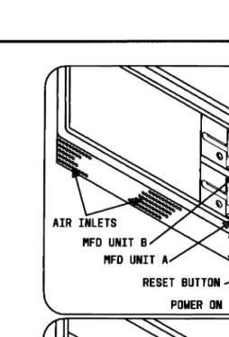
The System Module houses the Motherboard, Display Controller, Bus Converter Board, one or two slim (low profile) 5.25-inch Floppy Disk Units, and a Power Supply. Some System Modules may contain one Mini-Floppy Disk (MFD) Unit and a lO-MB or 20-MB slim HDU. If the Small Expansion Box or Slim HDU is present, the System Module will also contain a HDU Controller Board. All system modules are equipped with a fan.
AIR INLETS MFD UNIT B
MFD UNIT A
AIR INLETS HDU C
MFD UNIT A LATCH RESET BUTTON
[image:24.612.62.317.104.477.2]POWER ON LED
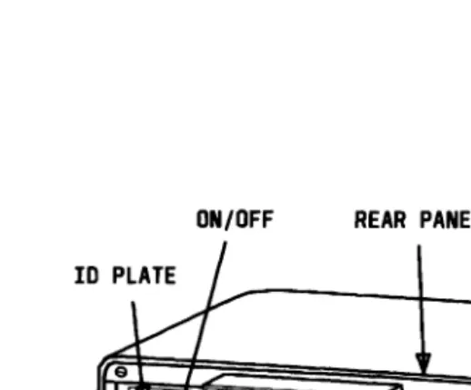
The rear panel of the System Module (Figure 2-3) consists of the following:
• Keyboard Connector
• Serial Port Connector
• Parallel Port Connector
• Power Inlet Connector
• Power Outlet Connector
• Display Connector
• On/Off Switch
• Access Slots for Expansion Boards
• Fan with Cover
REAR PANEL
I CONNECTOR
ACCESS SLOTS DISPLAY
, \
SERIAL \
]
FAN W/COVER
[image:26.611.73.332.201.415.2]KEYBOARD PARALLEL
Motherboard
RESET
o D D D D c=J c=J ~
DDDDDDDD~
0
c::JESESESES
0 0 0 c::Jb
D
DCIDDO CJ CJ c::J ~
c:::J D O D D c=:J CJ c:J CJ ~
0 0 0 0 0 I I c:::J CJ CJ c:::=J
c:::J ClOD 0 l---J 0 c=:J CJ ~
0 0 0 0
c=J
0 c=:J CJ ~ c:::J I I c:::::::J [III)]] CJ 0 c=:J CJ [III]]c:::::J c:::::::J c::J 0 c=:J CJ 0
c:::::J
I
I
c:::::::J c::::::J c:J 0 I 0c:::J c:::::::J I I 0 0
c:::J c:::::J c:::::J
D
0 c=J CJ CJD CJ c::::J CJ
o
c=J c=J c=:J CJ DD
mc=:J c=J c=:J c=:J D DDc=JillIIlCJI
IDc::JD
CJ
~CJCJ
CJCJCJ c:J c:JCJ
i
I
CJ CJ CJ [iilli] CIc::::::::J
DO
CIm
CI CI CI c::::J c:=::J CJ CJ _ C:=IITDJc=J CJ c=J c=:J c=J [iilli] CJ [ Ic=J c::::::J CJ CJ c:=J
[image:28.611.52.336.125.488.2]FAN
I)
""I/ojIll ORA~& PRO~
'"'' 1 CLi',24 CLJo.S ClII.4
1'(1815
RESE!
8086
8087 CPu NOP B" lS02 § ~ z
U
SSG!Jt-.---,
(IBAD 7
lJI'IAROV
M:
~
ADSTS
lJI'IAHLDA
O/'1AHRC
I)
DREl103 OACIl.Q 3CPU. NOP & O~AC
I
~
r-J,-,+i'r-rl-r+.-rrn...-~."'.,..,.,....""..,.-I· AOORS~-1
LATCH~1
P;\h"lllL PRl/oliER
1~llRFACl
SERIi\L
~
'7f
•
J
,
I/O PERIPHERAL INTERFACES!
.
,
110INTERfACE lr,<lERF"Cl
f!
I)
I
[image:29.842.55.628.111.499.2],
Figure 2-5. Functional Block Diagram of Motherboard
The Motherboard can be divided into four different sections with each section providing specific functions:
• Central Processing Unit (CPU) and Direct Memory Access (DMA)
• Memory - Random Access Memory (RAM) and Programmable Read-Only Memory (PROM)
• Input/Output (I/O) Peripheral Interfaces
• Input/Output Connectors.
These sections are connected by three system buses:
A Bus Carries address infornlation generated by the CPU or
DMA controller.
D Bus Carries data information between the CPU, DMA
controller, memory, and the I/O peripheral interfaces.
C Bus Carries all the control signals.
CP U and DMA Circuitry
The CPU used with the PC 6300 is the 16-bit Intel 8086-2 (or equivalent). This microprocessor contains the arithmetic and logic circuitry to extract program instructions from memory and execute them one at a time. The 8086-2 operates at a frequency of 8 MHz.
There is a socket on the Motherboard for an optional Numeric Data Processor (NDP). The NDP is a 16-bit Intel 8087-2 NDP (or equivalent) that serves as a co-processor attached to the 8086 CPU. The NDP monitors the 8086 instruction stream and extracts only the commands intended for the 8087. The 8087 NDP instructions include a full set of arithmetic functions as well as powerful exponential, logarithmic, and trigonometric functions.
The DMA circuitry on the Motherboard is constructed of:
• DMA Controller
• DMA Segment Register • DMA Control Buffer • DMA Data Buffer • DMA Address Latches.
Memory
The Motherboard RAM is organized in such a way that it can be addressed as bytes (8 bits) as well as words (2 bytes/16 bits). It is divided into two banks: bank 0 and bank 1. Both banks have two groups of nine 64-K or 256-K bit chips. One group is the lower byte (even address) and the other is the higher byte (odd address). Eight chips of each group are used for memory storage and the ninth chip is used for parity checking. All RAMs are dynamic and require periodic refresh. Memory refresh is provided by the DMA circuitry.
Input/Output Peripheral Interfaces
The 1/0 Peripheral Interfaces of the Motherboard are listed below:
• Keyboard Interface
• Mini-Floppy Disk Interface
• Parallel Printer Interface
• Serial Communications Channel (SCC) Interface
• 1/0 Chip Select Logic
• Interrupt Controller
• Timer
• Real-Time Clock and Calendar.
Keyboard Interface
Mini-FloPPY Disk Interface
The MFD Interface has two major functions:
• It manages the logic and control circuitry required in recording data onto and reading data from the MFD Units.
• It initially formats new disks.
Parallel Printer Interface
The Parallel Printer Interface provides one Centronics-like parallel interface for the connection of a printer. It is physically located on the Motherboard and access is made through the rear panel of the System Module. A printer may be one of the following:
• Daisy Wheel Letter-Quality Printer
• Dot-Matrix Printer.
Serial Communication Interface
The PC 6300 has a standard serial channel to support serial communications. The LSI serial communication chip used is the NEC 8250 (or equivalent). It provides one asynchronous RS-232 channel. The RS-232 connector is located on the Motherboard and access is made through the rear panel of the System Module.
Input/Output Chip Select Logic
Interrupt Controller
Hardware Interrupts are asynchronous events requiring CPU attention and are generally started by peripheral devices requiring service. The CPU is normally allowed to execute its main program until an interrupt request occurs. On receipt of an interrupt request, the CPU completes the instruction being executed, saves its current state (instruction pointer, code segment, and flags), and fetches a new routine to service the interrupting device. Once the interrupting device has been serviced, the CPU resumes its main program at the point wh2re it was interrupted.
Timer
The Timer is a programmable device that has three independent channels. Channel 0 is used as the input for the real-time clock. Channel 1 is used to time and request refresh cycles from the DMA channel. Channel 2 is used to support the tone generator for the audio speaker. The timer used is the Intel 8253 (or equivalent) programmable interval timer.
Real-Time Clock and Calendar
A Clock-Calendar Chip is used to provide real time such as seconds, minutes, hours, days, day of week, months, etc., for the system. A 3-volt, low-power standby rechargeable battery is connected to it to ensure that the real time is kept even when the system is turned off. The chip used is the MM58174AN.
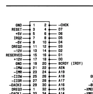
Input/Output Connectors
There are five I/O Connectors on the Motherboard. Two of the connectors (Jl and J2) are used to connect the Motherboard to the Display Controller. The other three connectors are for the
-~
~
~
~
~
~
~
~
~
~
~
- STROBE CD PTOOCD
82 PT01 CD
~
PT03W
PT05 CD PT07 CD BUSY o::D I J4 SLCT CID - ERROR~ - SLCTI 17 GNO CID
CD KB CLOCK GNO @
CD
GNO GNO ill>CD - RESET
GNO CID
m_
N_C_PARALLEl
CD
PT02CD PT04
m
PT08C@ - ACK
PE
ern-
_ ill) - AUTOFOX
ill) - INIT CID GNO
aID GNO ®GNO
ill) GNO
I)
~)
KEYBOARO PARALLEl SERIAL
J5 J4 J3
J2
82
COPlPONENT SlOE
J1
I : = : ~ GROUNO ..
~ ~ 015
AO CD ~
o
-BHE W~
o
-XPlEPllI~
CD
o
-XPlEPlRm
~o
-
XIOW o::D J1~
o
-XIOR CID~
o
-
EXTHRQ GID~
o
-
EXTACK CID~
o
OROY CID~
o
-INTA @~
~~
~
28 -PlB01S~ aID
BCCYL @ aID~---=I~NT'- 0
XCLKB W) 00
o
~
34"----+---00
m
38 CLK24 38KB OATA CD GNO 1 +12V CD KB-TYP WI J5 NC CD
CD
KEYBOARO
- CHCK 0
~
~
~
~
~
~
~
~
18 BCROY 0~
~
~
~
~
~
~
~
~
PRGNO RO CTS GNO -=T"""C RC ""'O:TPTR' CD CDW
CD-rn
o::Dl J3CIDGID CID ,CID @ ill> CID SERIAL TO
CD RTS
CD
OSRCD OCO
m
ill)
ern
i l l ) - ill)CID>-~OT:-::R'
aID RI ® TXCLK
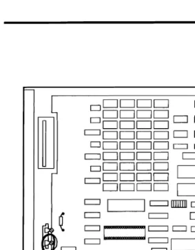
[image:39.844.103.630.104.507.2]Motherboard Component Layout
Figure 2-7 shows the physical location of the following principal Motherboard integrated circuits and other components:
1. 8086-2 CPU
2.8250 DART
3. Bank 0 RAM
4. Bank 1 RAM
5. High-Byte EPROM
6. Low-Byte EPROl\f
7. 8237 DMA Controller
8. 8259A Interrupt Controller
9. NEC /-LPD765 MFD Controller (or equivalent)
10. 8041 or 8741 Keyboard Controller
11. 8253 Timer
12. 8288 Bus Controller
13. Speaker
14. RESET Button
15. Battery
16. Clock-Calendar Chip
17. DIP Switch Bank 1
18. DIP Switch Bank 0
19. Z-8530 Socket
20. 8087-2 Socket
19 12 21 20 1
[image:41.612.43.343.163.464.2]10 11 B 9 18
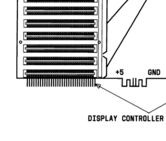
Display Controllers
The Three Display Controllers (Figures 2-8, 2-9, and 2-10) are designed to interface between the Motherboard and the Display. They attach in a perpendicular fashion to the Motherboard by the two lower connectors. The upper connectors are used for
connection of the Bus Converter Board.
PIGGY
BUS CONVERTER CONNECTOR BACK RETAINING BRACKET BOARD
DISPLAY CONNECTOR
RETAINING BUS CONVERTER CONNECTOR BRACKET
D
CIc=J
I10
Dc=J C J D
Dc=J C J D
Dc=J C J D
c=J C J D
1c=J C J D
CJ CJc=J
MOTHERBOARD CONNECTOR DISPLAY CONNECTOR
Figure 2-9. Display Controller (P4 Board)
PB BOARD RETAINING
(GO 380) BUS CONVERTER CONNECTOR BRACKET
The controllers have two basic modes of operation: alphanumeric and all points addressable graphics (with additional modes available within each of these). In the alphanumeric mode, the display can be operated either in a 40-column by 25-row mode or in an 80-column by 25-row mode. In both modes, character cell size is 8 dots (pixels) by 16 dots (pixels).
In the graphics mode, three resolutions are available:
• 640 by 400 pixels monochrome graphics
• 640 by 200 pixels monochrome graphics (IBM PC compatible)
• 320 by 200 pixels color graphics (IBM PC compatible).
The character attributes of reverse video, blinking, highlight, hide, and underline are available in the alphanumeric modes. In the color mode, 4 colors chosen from a palette of 16 can be displayed simultaneously. For a monochrome monitor, various shades of green are displayed to simulate a color display.
The display controllers contain 32 KB of arbitrated RAM for use as video refresh memory. The Display Controllers use a 6845 CRT controller. The 6845 controller operates at either 25 MHz, 19 MHz, or 12 MHz depending on the mode and resolution selected.
Bus Converter
The Bus Converter Boards (Figure 2-11) provides 16-bit and 8-bit expansion slots. This permits simultaneous use of 16-bit expansion boards and 8-bit IBM compatible expansion boards.
The Bus Converter Boards have two sets of connectors:
• Two or three 38-pin connectors to handle signals used by the 16-bit expansion boards.
• Seven 62-pin connectors to handle signals used by both 16-bit boards and 8-bit IBM compatible boards.
Figure 2-11 shows that the connectors are arranged in seven rows. Two or three of the rows have both a 38-pin and a 62-pin connector in the row. These rows are used to connect the 16-bit expansion boards to the system and are referred to as dual-connector
expansion slots. One dual-connector expansion slot is reserved for a Video Enhancement Board (DEB [Display Enhancenlent
Board]). The other is used for the insertion of a Memory Expansion Board that is discussed later in this chapter.
Figure 2-11 also shows that there are five remaining rows with one 62-pin connector. These five expansion slots are used to install 8-bit IBM compatible boards. They are referred to as
SINGLE EXPANSION SLOTS DUAL EXPANSION SLOTS
o
o
o
o
DISPLAY CONTROLLER CONNECTORS
SINGLE EXPANSION SLOTS
o
DUAL EXPANSION SLOTS
o
o
o
o
[image:47.611.44.326.262.501.2]Input/Output (I/O) Expansion Bus
Characteristics
GND RESET +5V IRQ2 -5V DREQ2 -12V RESERVED +12V GND -IMW -IMR -IIDW -IIOR -DACKS OREQS -DACK1 OREQ1 -DACKO XClK4 IRQ7 IRQ6 IRQ5 IRQ4 IRQ3 -DACK2 TC ALE +5V 14 MHz GND -CHCK 07 06 D5 04 03 02 01 DO BCRDY AEN A19 A18 A17 A16 A15 A14 A13 A12 A11 A10 A9 A8 A7 A6 A5 A4 A3 A2 A1 lAO (IRDY) GND AD -BHE -XMEMW -XMEMR -XIOW -XIOR -EXTHRQ -EXTACK -ORDY -INTA CASO CAS1 CAS2 RESERVED XCLK8 +5V GND RESERVED GNO 015 014 013 D12 011 D10 D9 08 -BSO -BS1 -BS2 -16BCH -f'lBDIS RESERVED -INT +5V GND Z8000CLK
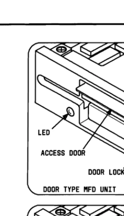
Mini-Floppy Disk Unit(s)
The AT&T Personal Computer 6300 uses 5.25-inch MFD Units (Figure 2-13) that have a formatted capacity of 360 KB. Refer to the "AT&T Personal Computer 6300 Reference Manual" for
DOOR TYPE MFD UNIT
[image:51.612.80.299.116.496.2]LATCH TYPE MFD UNIT
Slim Hard Disk Units (Optional)
lO-MB Hard Disk Unit
One of the MFD Units may be replaced with a 10-MB (formatted) Hard Disk Unit (HDU). The HDU (Figure 2-14) is a random access 5.25-inch slim (half-height) Winchester storage device with two nonremovable disks as storage n1edia. Each disk surface has one movable head to service 306 data tracks. This Slim HDU is the same physical size and mounts the same as the MFD Unit. It also uses the same dc voltages as the MFD Unit. The installation of this HDU requires a minimum of 256-KB RAM.
20-MB Hard Disk Unit
Hard Disk Unit Controllers (Optional)
If a HDU is added to the system (internally or externally), the HDU Controller (Figure 2-15) or (Figure 2-16) must be installed to interface the HDU with the 8086 CPU. The HDU Controller is a circuit board that plugs into one of the 8-bit expansion slots on the Bus Converter. It is attached to the HDU with two ribbon cables. Refer to "Appendix A" for information on how to configure the HDU controller.
There are two types of HDU Controllers, the DTC (Data Technology Corporation) and the WD (Western Digital). The physical differences between the Controllers are:
1. The DTC Controller is a full-size modular circuit card. The WD Controller is a half-size modular circuit card.
2. Each HDU Controller must be configured for the type of drive used (see Appendix A). The DTC Controller is configured by setting the DIP Switches on the card. The WD Controller has jumpers that must be placed.
Each Controller formats the hard disk drives differently; therefore, they cannot be interchanged without performing the following:
• Make a backup copy of all data if possible
• Low-Level Format the drive using the System Test
• Partition the drive using the MS-DOS FDISK
The WD Controller is not supported by ROM BIOS 1.21 and earlier versions. Both the DTC and the WD Controller are supported by ROM BIOS 1.43 and later versions.
MOUNTING BRACKET DIP SWITCHES
(NOTE)
ESC]
c=J2c=Ji_-
....----~---.
~
C]~~c=JI
__
DCJ C]~~CJ I
CJ
c=J c=J~ ~
c=J====~
CJI
I
CJCJCJC]I_-CJ
CJ CJC=I CJ CJ CJNOTE: DIP SWITCHES ARE MOUNTED LOWER ON SOME REVISIONS OF THE HDU CONTROLLER
Figure 2-15. DTC Hard Disk Unit Controller
The J1, J2, and J3 connectors on the DTC Controller provide the following:
• The J1 connector is the control connector. This connector transfers the control signals to and from the HDUs. Two HDVs
can be installed using a Daisy Chain Connection.
MOUNTING
J3 J2 J1 BRACKET
JUMPER BLOCK
Figure 2-16. Western Digital Hard Disk Unit Controller (Requires a ROM BIOS 1.43 or Higher)
The Jl, J2, and J3 connectors on the WD Controller provide the following:
• The Jl connector is the control connector. This connector transfers the control signals to and from the HDUs. Two HDUs can be installed using a Daisy Chain Connection.
Memory Expansion Board (Optional)
The Memory Expansion Board (Figure 2-17) is organized in three banks of 128 KB each. The three banks (0, 1, and 2) are each made up of two groups of nine 64-K bit RAM chips. One group is the lower byte (even address) and the other is the higher byte (odd address). Eight chips are used for memory and the ninth chip is used for parity checking.
iii
iii
iiiiiiiii
IiIii
iiiiii
1::1
=
=
0o
===
888880888
1:1
1::1
1:1
=
o
==
1::1
=
lC
l:IeI
=
1::=
I:ia
The Memory Expansion board is inserted in a 16-bit expansion slot on the Bus Converter Board. The minimum amount of memory on the Memory Expansion Board is 256 KB (128 KB in bank 0 and 128 KB in bank 1). This can be expanded up to 384 KB by inserting chips into bank 2. The Motherboard must have 256-KB RAM before the Memory Expansion Board can tJe used.
Power Supply
The Power Supply is the metal box found at the rear of the System Module between the disk drives and the fan. The PC 6300 uses a switching-type LA16 or LAI6/B power supply with the following electrical input characteristics:
• Single-phase alternating current for the two ranges 100 to 120 V and 200 to 240 V. This is done using a main voltage changeover jumper mounted on the printed circuit board, a different line cord, and fan assembly. The total power output is 163 Watts (LAI6) or 182 Watts (LAI6/B).
• Permanent driftings of the nominal voltage ± 10%, that allows two ranges of correct operation: 90 to 132 V and 180 to 264 V. The transient driftings are shown in Figures 2-18 and 2-19.
• Nominal operating frequency of 50 and 60 Hz with acceptable variations of ± 5%.
The only voltage calibration potentiometer present on the power supply is for the +5 V dc. Any variation of the +5 V dc will also affect the
+
12, -12, and+
15 V dc. Figure 2-20 shows the power supply output voltages and the potentiometer location.LAI6/B POWER SUPPLY
The general output specifications for the LA16/B power supply is shown in the following table (Figure 2-18). It shows the minimum and maximum values of current generated per the output voltages. The power supply unit is able to provide a stationary power of 182 watts.
Nominal
Voltage Tolerance
Minimum Current Maximum Current Maximum Ripple
+5 V ±5% 6.2 A 20.8 A 50 mVp-p
+12 V (Note) ±5% 0.9 A 4.2 A 100 mVp-p
+15 V ±10% 1.0 A 1.8 A 250 mVp-p
-12 V ±5% 0 0.25 A 100 mVp-p
Figure 2-18. Power Supply Output Characteristics
Note: An inlpulsive repetitive load with maximum 1/5
duty cycle and behavior is allowed on the +12 V. An impulsive load is allowed on the +12 V to be added to the static load in the power-on transition where a deviation from the rated tolerances of the output voltages is allowed. The worst load crossings allowed with no power take-off on
+
15 V are as follows:1(+12 V) 0.9 A (min) I (+5) 14.3 A (max)
LA16 POWER SUPPLY
The general output specifications for the LA16 power supply is shown in the following table (Figure 2-19). It shows the minimum and maximum values of current generated per the output voltages. The power supply unit is able to provide a stationary power of 163 watts.
Nominal
Voltage Tolerance
Minimum Current Maximum Current Maximum Ripple
+5 V ±5% 6.2 A 16.8 A 50 mVp-p
+12 V (Note) ±5% 0.9 A 4.5 A 100 mVp-p
+15 V ±10% 1.0 A 2.4 A 250 mVp-p
-12 V ±5% 0 0.25 A 100 mVp-p
Figure 2-19. Power Supply Output Characteristics
Note: An impulsive repetitive load with maximum 1/5 duty cycle and behavior is allowed on the +12 V. An impulsive load is allowed on the +12 V to be added to the static load in the power-on transition where a deviation from the rated tolerances of the output voltages is allowed. The worst load crossings allowed with no power take-off on
+
15 V are as follows:I (+12 V) 0.9 (min) I (+5) 14.3A (max)
-12V MOTHERBOARD ( +12V
DISPLAY (
CONTROLLER
~:~~
BOARD +1
I
~~
I
IUUUU'~
SYSTEM BOARDS , GND +5V'
_ _ _
;~~V]
INTERNAL_ - GND DRIVES
+5V
;~~V]
~~~~~SION
~.
GND BOX [image:63.612.45.353.182.435.2]r
+5VThe optional Display Enhancement Board provides additional operating modes when used with the Display Controller Board. The main features provided by the Display Enhancement Board are:
1. Three additional 640 x 400 pixel bit planes-higher resolution with 16 colors.
2. Two new graphic modes that support up to 16,536 colors/patterns:
• 640 x 400 pixels color graphics-16 colors on screen (16 shades of green on monochrome display)
• 640 x 200 pixels color graphics-16 colors on screen (16 shades of green on monochrome display).
3. Software-controlled color look-up table:
• Maps bit planes to 16-color palettes-allowing color cycling
• Supports 4 blink rates in hardware
• Supports dithering in hardware
4. Simultaneous display of characters and graphics.
5. Simultaneous use of either a Monochrome and Color Display or two Color Displays. (The System Module Power Supply will not support the simultaneous use of two Monochrome
Displays.)
6. Compatibility between the Display Enhancement Board (in the transparent mode) and the IBM PC graphics software.
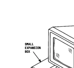
A Small Expansion Box (Figure 2-21) can be connected to the PC 6300 to provide the PC 6300 with additional disk storage. The Small Expansion Box contains a 10-MB (formatted) HDU. The HDU Controller is housed in the System Module on the Bus Converter Board. This external HDU is connected to the HDU Controller by two ribbon cables. The Small Expansion Box also contains a fan to cool the HDU. The Small Expansion Box can be used with either one or two MFD Units and requires a minimum of 256-KB RAM.
Monochrome Display
Color Display (Optional)
Either of the two Color Displays (Figures 2-23 and 2-24) attach to the System Module with two cables: a signal cable and a power cable. The Display may sit on top of the System Module or on a nearby table or desk. The Color Displays can display up to
16 different colors with the red, green, and blue video signals (and intensity) independent of each other.
[image:69.612.77.325.244.528.2]There are two types of Keyboards that can be used with the AT&T Personal Computer 6300. They are the Model 301 Keyboard
(Figure 2-25) and the Model 302 Keyboard (Figure 2-26). Both Keyboards have two different positions that can be adjusted to suit the operator; each Keyboard can be tilted 4 or 8 degrees. The Keyboards have a permanently attached cable that connects to a connector at the rear of the System Module. This shielded cable has 5 wires:
+
12 V dc, 2 Grounds, and 2 bidirectional signal lines. The cable is approximately 6-feet long and is coiled like that of a telephone handset. The central (alphanumeric) part of the [image:71.611.37.344.329.541.2]Keyboard is standard. There are 10 function keys on the left of the Model 301 Keyboard. The function keys on the 302 Keyboard are located in a row on top of the Keyboard. Both Keyboards have 15 numeric keys on the right-hand side that have legend for their numeric functions, cursor control, numeric calculations, and display editing. Both Keyboards support the AT&T Mouse 6300.
The PC 6300 contains the following in its minimum configuration:
a. Monochrome Display
b. Keyboard
c. System Module 1. Motherboard
• 16-KB EPROM • 128-KB RAM • 8-MHz 8086-2 CPU • DMA Controller • Floppy Disk Interface • Timer
• Interrupt Controller
• Serial Communication Controller (one channel- asynchronous)
• Parallel Interface
• Battery Back-Up Calendar Chip • Keyboard Controller
2. Display Controller 3. Bus Converter
4. One 5.25-inch (360-KB) MFD Unit 5. Power Supply
The PC 6300 can be expanded with the insertion of option boards in the System Module or installing external options. In its expanded configuration, the PC 6300 may contain the following:
a. Color Display
b. Keyboard with Mouse
c. System Module 1. Motherboard
• 8087 Math Co-Processor • 16-KB EPROM
• 640-KB RAM • 8-MHz 8086-2 CPU • DMA Controller • Floppy Disk Interface • Timer
• Interrupt Controller
• Serial Communication Controller (one channel- asynchronous)
• Parallel Interface
• Battery Back-Up Calendar Chip • Keyboard Controller
2. Display Controller 3. Bus Converter Board
• Memory Expansion Board • HDU Controller
4. Display Enhancement Board (DEB)
5. Two 5.25-inch (360-KB) MFD Units or One MFD Unit and One Slim HDU
d. Small Expansion Box (Full-Size lO-MB HDU)
ENVIRONMENTAL
REQUIREMENTS...
3-5PHYSICAL CHARACTERISTICS. . .
3-6UNPACKING.. .. .. . .. .. .. .. .. .. . .. . .. . .. . . ..
3-7OPTION INSTALLATION...
3-8Upgrading Motherboard Memory to 256KB or
Upgrading Memory Expansion Board Memory to
Replacing Mini-Floppy Disk Unit With Hard Disk
Removing System Module Covers. . . 3-9 Removing Upper Cover. . . 3-10 Removing Lower Cover . . . 3-11
640KB 3-12
Installing Memory Expansion Board . . . . . . . . . . . . 3-21
384KB 3-27
Installing 8087 Numeric Data Processor 3-36 Unit. . . 3-42
Removing Upper MFD Unit 3-42
Installing the Mouse
Installing the Ball in the Mouse Connecting the Mouse to the Computer
Installing the Keyboard ROM Opening the Keyboard Removing Existing ROM Chip Installing New ROM Chip
Installing the Mouse Software
. 3-100
. 3-100
. 3-102
. 3-104
. 3-104
. 3-105
. 3-105
. 3-107
Installing the Mouse Software With the Dual Diskette
Computer . 3-107
Installing Mouse Software With the Hard Disk
Computer . 3-109
SYSTEM INSTALLATION
.
3-110APPLYING POWER TO THE
The AT&T Personal Computer 6300 operates reliably in a typical office environment, but it is important to adhere to the following when choosing a suitable site:
1. The PC 6300 should be plugged into a grounded outlet.
Ungrounded machines do not work properly and can be a safety hazard. If the PC 6300 is not plugged into a grounded outlet, one can experience:
• Improper program operation • Unreadable disks
• Extensive machine damage.
The PC 6300 should, when possible, be isolated from sources of electrical noise and from devices that can cause excessive voltage level variations. Some common sources of electrical noise are:
• Air conditioners, fans, refrigerators, washing machines, and large blowers
• Transfornlers and alternators
• Large brush-type or induction motors (such as those used on elevators)
• Radio and TV transmitters, microwaves, signal generators, and high-frequency security devices.
2. The PC 6300 should be placed in a dust-free
environment. Airborne dust, dirt, and smoke can cause excessive wear on moving surfaces, short open circuits (especially in the presence of high humidity), and read/write errors on the disk.
3. The PC 6300 should be placed away from heat and direct sunlight. Unusually high temperatures coupled with low humidity can cause static problems.
4. The front and rear panels of the PC 6300 should not be obstructed. The PC 6300 is cooled by a fan located on the rear panel. This fan pulls air in through air inlets on the base of the System Module. The base of the System Module should be free from papers or other materials that would obstruct air flow.
The environment in which the PC 6300 operates should meet the following requirements:
Electrical
100-120 (standard); 200-240 volts maximum (selectable by an internal power supply jumper)
50-60 Hertz
Power usage - 162 watts
Ambient Temperature
Operating: + 10 to +40 degrees Centigrade (+50 to +104 degrees Fahrenheit) Storage: -40 to +60 degrees Centigrade
(-40 to +140 degrees Fahrenheit)
Relative Humidity
Operating: 10% to 95% RH, noncondensing Storage: 5% to 95% RH, noncondensing
Altitude
Operating: Sea Level to 10,000 feet Storage: Sea Level to 30,000 feet
Standards
UL 478 and 114 CSA 154 and 143
FCC Part 15, Subpart J, Class B
Acoustic Noise Level
The System Module [with two Mini-Floppy Disk (MFD) Units] weighs 30.8 lbs. (14 Kg), the Display weighs 19.8 lbs. (9 Kg), and the Keyboard weighs 4.5 lbs (2 Kg).
Figure 3-1 lists the approximate physical dimensions and weight of the System Module, the Monochrome and Color Displays, and Model 301 and Model 302 Keyboards.
APPROXIMATE PHYSICAL CHARACTERISTICS
UNIT SIZE WEIGHT
System Module 15" x 14V2" x 6" 38.1 em x 36.8 em x 15.2 em
30.8Ibs. 13.8 kg Monochrome Display 13" x 12 1h" x 10th"
33.0 em x 31.3 em x 26.3 em
19.8Ibs. 9.0 kg Color Display 14" x 14" x 14 1/2"
35.6 em x 35.6 em x 36.8 em
271bs. 12. kg Model 301 Keyboard 17V2" x 7V2" X 1"
40.6 em x 19.1 em x 2.5 em
41/2 Ibs. 2. kg Model 302 Keyboard 16" x 81/2" x 1%"
44.5 em x 19.1 em x 2.5 em
4V2 Ibs. 2. kg
PROTECT YOUR HARD DISK
To prevent damage to CPU's with hard disks, always park the HDU by using the "SHIP" command which is found on the enclosed System Test Diagnostics Diskette before moving. See additional information on the following page.
The three main units of the system are the System Module, the Display, and the Keyboard. These units are packed in protective packaging before being placed in a shipping carton. The packaging protects the modules against damage during transit. The shipping carton should also contain the ac Power Cable that is used to connect the system to the grounded wall outlet.
This section gives the installation procedures for various options supported by the PC 6300. If no options are to be installed, go to the section titled "System Installation." If options are to be installed, it is much easier to install them before connecting the major units for system operation. Please keep in mind that the procedures for installing options are presented as though the PC 6300 is operational and that only one option is being installed at a time.
During the installation of many options, the System Module must be shifted into various positions to allow access to certain parts of the module. When handling the System Module, care should be taken not to damage its components in any way. If the System Module contains a HDU, extra care should be taken because the HDU is sensitive to sudden shocks. Before moving the unit, the HDU heads should be parked, using the "SHIP" command. If power is present on the HDU, the Systenl Module must never be lifted for any reason.
Before attempting to install any of the options, one should become familiar with the Dual In-Line Package (DIP) switches and jumpers associated with most options. Appendix A provides information on the location of the system's DIP switches and jumpers and how they should be set for the various system configurations. At this point, it may be helpful to remove the System Module covers to view the DIP switches and jumpers while reviewing Appendix A.
Removing System Module Covers
Removing Upper Cover
[image:86.612.91.290.224.350.2]1. Loosen the two screws that secure the upper cover (Figure 3-2).
~---~_/
Figure 3-2. Removal of the Upper System Module Cover
Removing Lower Cover
1. Turn the System Module upside down so that the lower cover is on top.
[image:87.612.105.298.265.385.2]2. Loosen the two screws that secure the lower cover (Figure 3-3).
Figure 3-3. Removal of the Lower System Module Cover
Upgrading Motherboard Memory to 256 KB or
640KB
The materials required for upgrading the Motherboard memory are:
• Eighteen 64-K bit or 256-K bit RAM chips (see the following table)
• Medium-sized standard screwdriver.
VARIOUS CONFIGURATIONS NEW UPGRADED CONFIGURATION 18 RAM Chips
in Bank 0 (Each)
Total Memory Add 18 RAM Chips to Bank 1 (Each)
Total New Memory
64 KB 64 KB 256 KB
128 KB 128 KB 512 KB
64 KB 256 KB 64 KB
Caution: To prevent any damage to the system circuitry by static electricity, be sure to wear a wrist static strap or touch the metal chassis of the system just before you handle any IC chips or system boards.
To upgrade the Motherboard memory, proceed as follows:
1. Turn the System Module and all external devices OFF.
2. Unplug the ac power cable from the rear panel.
3. Disconnect all cables (Display, Keyboard, Printer, etc.) from the rear panel of the System Module.
4. Turn the System Module upside down so that the lower cover is on top.
5. Loosen the two screws that secure the lower cover (located on the rear panel).
7. Locate Bank 1 on the Motherboard (Figure 3-4).
[image:90.611.59.345.157.372.2]FRONT RIGHT-HAND CORNER
Figure 3-4. Locating Bank 1 on the Motherboard
9. Align the RAM chip pins (A) with a socket (B) as in Figure 3-5. Make sure that the notch in the chip (C) is facing the same direction as the other chips on the board. To insert, push the chip down firmly.
c
A
Figure 3-5. Inserting RAM Chip into the Socket
10. Repeat Step 8 for the remaining 17 sockets in Bank 1 of the Motherboard memory.
12. Locate DIPSW-0 on the Motherboard (Figure 3-6).
I§§§§§§§§I
~b::::::d
I§§§§§§§§I
DIPSW-1 DIPSW-O
I
c:::::::::Jc:::::::::Jc:::::::::Jc:::::::::J c::::J c::::J c::::J c:==J c::::Jo
c:::::J c:::::JI
I
c:::::Jc::::J c::::J r - - - l c::::J c::::J c::::J c=J
c::::J c=J
~
c=J0
0
I
I
C=:J c=J c=J c=J c=J C=:J c:::::::::J c:::::::::J c:::::::::J
[image:92.612.65.351.177.408.2]I==:J c=J C=:J c=J c=J c::::J c::::J c:::::::::J
D
c:::::::::JFigure 3-6. Locating DIPSW-0 on the Motherboard
13. On DIPSW-0, set switches 1, 2, 3, and 4 for 256-KB total memory (Figure 3-7).
• Switch 1 ON • Switch 2 OFF • Switch 3 ON • Switch 4 ON
• Switches 5 to 7 (Do not require setting for memory) • Switch 8 OFF.
1
2
3
4
5
6
7
8
x
o
N
1
x
x
o
Figure 3-7. DIPSW-O Setting for 256-KB Total Memory
Note: Some switches are rocker type; others are slide type. Some DIP switches have the ON designation at the top of the switch; others have it on the bottom.
14. On DIPSW-0, set switches 1, 2, 3, and 4 for 640-KB total memory adding 256-K bit chips (Figure 3-8).
• Switch 1 OFF • Switch 2 ON • Switch 3 OFF • Switch 4 OFF
• Switches 5 to 7 (Do not require setting for memory) • Switch 8 OFF.
1
2
3
4
5
6
7
8
o
N
x
x x o
f
Figure 3-8. DIPSW-0 Setting for 640-KB Total
Memory on Motherboard Using 256-K
Bit Chips in Bank 1
Note: Some switches are rocker type; others are slide type. Some DIP switches have the ON designation at the top of the switch; others have it on the bottom.
15. On DIPSW-0, set switches 1, 2, 3, and 4 for 640-KB total menlory adding 64-K bit chips (Figure 3-9).
• Switch 1 OFF • Switch 2 ON • Switch 3 ON • Switch 4 OFF
• Switches 5 to 7 (Do not require setting for memory) • Switch 8 OFF.
1
2
3
4
5
6
7
8
o
N
x
x
x
o
f
Figure 3-9. DIPSW-0 Setting for 640-KB Total
Memory on Motherboard Using 64-K
Bit Chips in Bank 1
Note: Some switches are rocker type; others are slide type. Some DIP switches have the ON designation at the top of the switch; others have it on the bottom.
16. Replace the lower System Module cover and tighten the two cover screws.
17. Place the System Module back to its upright position.
18. Connect the cables that were disconnected (Keyboard, Display, Printer, etc.) back to the rear panel of the System Module.
19. Plug the ac power cable into the rear panel.
Installing Memory Expansion Board
The Motherboard memory ~ust be fully populated (256 KB) before installing the Memory Expansion Board. The Memory Expansion Board is equipped with a minimum of 256-KB RAM and can be expanded to 384 KB maximum. This will supply the system with a total of 512-KB or 640-KB RAM, respectively. If the Memory Expansion Board is to be expanded to 384 KB, refer to the section titled "Upgrading Memory Expansion Board to 384 KB" before installation.
The materials required for the installation of the Memory Expansion Board are:
• Medium-sized standard screwdriver • Memory Expansion Board.
Caution: To prevent any damage to the system circuitry by static electricity, be sure to touch the metal chassis of the system just before you handle any IC chips or system boards.
To install the Memory Expansion Board, proceed as follows:
1. Turn the System Module and all external devices OFF.
2. Unplug the ac power cable from the rear panel.
4. Turn the System Module upside down so that the lower cover is on top.
5. Loosen the four screws that secure the upper and lower covers (located on the rear panel).
6. Slide the lower cover forward approximately 0.5 inch and lift it from the System Module.
7. Locate DIPSW-O on the Motherboard (Figure 3-10).
I§§§§§§§§I
~b::::::J
I§§§§§§§§I
c:::J c::::J
'1'---1 "-~c::::=J c:::=::J c::::J c::::J
c=J~~1
c=JDDI
DIPSW-1
1
o
c:::::JDIPSW-O
c:::::=:J c:J
I
~
I
c:=:J c:=:J c:::::J c:::::J c::::J c:=J c::::J c::::J ~
[image:98.612.71.356.294.525.2]c:::::J c:::::J c:::::J c:=::J c=J c=J c=:J c::==:J
D
c::::Jo
1
2
3
4
5
6
7
8
N
1
x
x
x
o
8. On DIPSW-O, set switches 1, 2, 3, and 4 for 512-KB Total RAM (Figure 3-11).
• Switch 1 ON • Switch 2 ON • Switch 3 OFF • Switch 4 ON
• Switches 5 to 7 (Do not require setting for memory) • Switch 8 OFF.
Figure 3-11. DIPSW-O Setting for 512-KB Total RAM in System (256 KB on
Motherboard, 256-KB Memory Expansion Board)
Note: Some switches are rocker type; others are slide type. Some DIP switches have the ON designation at the top of the switch; others have it on the bottom.
9. Replace the lower System Module cover and tighten the two screws that secure the cover.
10. Place the System Module back to its upright position.
11. Slide the upper cover forward approximately 0.5 inch and lift it from the System Module.
[image:100.611.44.331.291.485.2]12. Using a screwdriver, remove the Expansion Slot Cover of the second dual connector expansion slot (Figure 3-12).
13. Put on the wrist strap and connect to ground (if available), or touch the metal chassis before picking up the Memory Expansion Board to release the static electricity from your hand.
[image:101.611.53.355.223.541.2]14. Gently insert the Memory Expansion Board into the first dual connector expansion slot on the Bus Converter Board (Figure 3-13).
15. Remove the wrist strap (if wrist strap was used).
16. Using a screw and screwdriver, secure the Memory
Expansion Board by fastening the retaining bracket to the rear panel.
17. Replace the upper System Module cover and tighten the two cover screws.
18. Connect the cables that were disconnected (Keyboard, Display, Printer, etc.) back to the rear panel of the System Module.
19. Plug the ac power cable into the rear panel.
Upgrading Memory Expansion Board Memory
to
384 KB
The materials required for the upgrade of the Memory Expansion Board memory to 384 KB are:
• Eighteen 64-K bit RAM chips
• Medium-sized standard screwdriver.
Caution: To prevent any damage to the system circuitry by static electricity, be sure to touch the metal chassis of the system just before you handle any IC chips or system boards.
To upgrade the Memory Board, proceed as follows:
1. Turn the System Module and all external devices OFF.
2. Unplug the ac power cable from the rear panel.
3. Disconnect all cables (Display, Keyboard, Printer, etc.) from the rear panel of the System Module.
6. Turn the System Module upside down so that the lower cover is on top.
7. Slide the lower cover forward approximately 0.5 inch and lift it from the System Module.
8. Locate DIPSW-O on the Motherboard (Figure 3-14).
I§§@@@@@§I
~b::::::J
I§§@@@@@§I
DIPSW-1 DIPSW-O
I c=::J c:::=:::J c=::J c:::=:::J
- - - L...----tl---t L-..7fI&--' c:::::=:J c::=J c:::::=:J [==:J c:::::=:J
~
c:=J r - l c:=J~~I
I
~
c:::J c:::J L - J c:::J
D D
I
I
c::=J c::::J c::::J c::::J c::=:J c=J c:::::=:J r:=:=:J c = J
[image:104.611.61.353.226.470.2]c::::J c::=:J c::::J c::::J c:=J c=J c::::J c::::::J
D
c = J9. On DIPSW-O, set switches 1, 2, 3, and 4 (Figure 3-15).
• Switch 1 OFF • Switch 2 ON • Switch 3 OFF • Switch 4 ON
• Switches 5 to 7 (Do not require setting for memory) • Switch 8 OFF.
1
2
3
4
5
6
7
8
o
N
x
x
x
o
f
Figure 3-15. DIPSW-O Setting for 640-KB Total Memory in System (256 KB on Motherboard, 384 KB on Memory Expansion Board)
Note: Some switches are rocker type; others are slide type. Some DIP switches have the ON designation at the top of the switch; others have it on the bottom.
ON=CLOSED= 1
10. Replace the lower System Module cover and tighten the two screws that secure the cover.
11. Place the System Module back in its upright position.
12. Remove the screw that secures the Memory Expansion Board retaining bracket to the rear panel.
14. Remove the Memory Expansion Board from the Bus Converter (Figure 3-16).
15. Locate Bank 2 on the Memory Expansion Board (Figure 3-17).
16. Align the RAM chip (A) with a socket (B) as shown in Figure 3-18. Make sure that the notch in the chip (C) is facing the same direction as the other chips on the board. Push the chip down firmly to insert.
c
A
Figure 3-18. Inserting the RAM Chip into the Socket
18. Gently insert the Memory Expansion Board into the first dual connector expansion slot on the Bus Converter Board (Figure 3-19).
19. Remove the wrist strap (if wrist strap was used).
20. Secure the Memory Expansion Board by fastening the retaining bracket to the rear panel.
21. Replace the upper System Module cover and tighten the two cover screws.
22. Connect the cables that were disconnected (Keyboard, Display, Printer, etc.) back to the rear panel.
23. Connect the ac power cable to the rear panel.
Installing 8087 Numeric Data Processor
The 8087 Numeric Data Processor (NDP) is a fast arithmetic processor that serves as a co-processor to the 8086 CPU. The 8087 NDP is installed into a socket on the Motherboard next to the 8086. The materials required for installing the 8087 NDP are:
• Medium-sized standard screwdriver
• 8087 NDP.
Caution: To prevent any damages to the system circuitry by static electricity, be sure to touch the metal chassis of the system just before you handle any IC chips or system boards.
To install the 8087 Numeric Data Processor, proceed as follows:
1. Turn the System Module and all external devices OFF.
2. Unplug the Module's power cable from the ac wall outlet.
4. Turn the System Module upside down so that the lower cover is on top.
5. Loosen the two screws that secure the lower cover (located on the rear panel).
6. Slide the lower cover forward approximately 0.5 inch and lift it from the System Module.
DIP 8087 NOB
[image:114.611.46.325.116.411.2]SWITCHES SOCKET 808SCPU
Figure 3-20. Locating the 8087 NDP Socket
9. Align the 8087 NDP pins with the socket. Make sure that the notch in the chip is pointing in the same direction as other chips on the Motherboard. Then gently insert the 8087
NDP into the socket.
10. Renl0ve wrist strap (if wrist strap was used).
11. Locate DIPSW-O on the Motherboard (Figure 3-21).
I§~@@@@@§I
~6::::::d
DIPSW-1
I§~@@@@@§I
DIPSW-OI c::::::::J c::::::::J c::::::::J c::::::::J
i1'---t 1"""""""'----1 c::::J c:::::::J c::::::::J c:::::::J c:::::::J
~
c : : J , - - - , c::J~~
I
I
~
c::J c::J L..-J c::J
D D
I
I
c:::J c:::J c::::::J c::::::J c::::::J c:::::J c:::::::J c::::::::J c:::::::J
[image:115.611.67.359.248.483.2]c::::::J c:::::J c::::::J c::::::J c::::::J c::::J c::::J c::::::::J
D
c::::::::J12. Set DIP switch 5 as shown in Figure 3-22.
• Switches 1 to 4 (Do not require setting) • Switch 5 OFF
• Switches 6 to 8 (Do not require setting).
1
2
3
4
5
6
7
8
o
N
x
x
x
x
o
x
x
x
r
Figure 3-22. Setting DIPSW-0 for Presence of 8087 NDP
Note: Some switches are rocker type; others are slide type. Some DIP switches have the ON designation at the top of the switch; others have it on the bottom.
13. Replace the lower System Module cover and tighten the two cover screws.
14. Place the System Module back to its upright position.
15. Connect the cables that were disconnected (Keyboard, Display, Printer, etc.) back to the rear panel of the System Module.
16. Connect the system power cable to the System Module and then to t