Effect of Thermal Cycles on Microstructure of Er
2O
3Thin Film on SUS316
Substrate with Y
2O
3Buffer Layer Fabricated by MOCVD Method
Masaki Tanaka
1, Seungwon Lee
2, Kenji Matsuda
2,*, Yoshimitsu Hishinuma
3, Katsuhiko Nishimura
2,
Teruya Tanaka
3and Takeo Muroga
31Graduate School of Science and Engineering for Education, University of Toyama, Toyama 930–8555, Japan 2Graduate School of Science and Engineering for Research, University of Toyama, Toyama 930–8555, Japan 3National Institute of Fusion Science, Toki 509–5292, Japan
Erbium oxide (Er2O3) and Yttrium oxide (Y2O3) are the promising materials to realize an advanced breeding blanket system because of
good electrical resistivity and effective hydrogen permeation suppression. In this report, Er2O3 thin film fabricated via MOCVD process with
the Y2O3 layer formed on SUS316 substrate before and after thermal cycles to investigate the effect of thermal cycling. Their microstructure
was confirmed by SEM, AFM, TEM and STEM. The surface morphology of samples after thermal cycling has small granular structure than samples before thermal cycling and without buffer layer. According to cross sectional observation by TEM and STEM, Er2O3 and Y2O3 have
different columnar structure, while buffer layer did not avoid diffusing elements from SUS316 substrate to Er2O3 layer. The thermal cycling
test had not been affected to the growth direction of Er2O3 and Y2O3 layers, which is mostly cube-cube relationship.
[doi:10.2320/matertrans.MC201710]
(Received June 27, 2017; Accepted August 22, 2017; Published September 29, 2017)
Keywords: erbia, yittria, microstructure, transmission electron microscopy
1. Introduction
In advanced breeding blanket system of nuclear fusion re-actor, it needs to develop advanced type of coating to leak control of tritium and reduce Magneto Hydro-Dynamic (MHD) pressure drop1). Component materials in this system have been required to optimize conditions, for example, no breakdown at high temperature, high electrical resistivity of MHD pressure drop, and so on. Erbium oxide (Er2O3) coat-ing was selected as the one of the most promiscoat-ing materials in ceramic coating to restrict MHD effect and tritium perme-ation on advanced breeding blanket system.1,2) Er
2O3 film has been formed on the surface of SUS316 steel pipe by Metal organic chemical vapor deposition (MOCVD) method by our co-worker of Hishinuma et. al., and its microstructure has been investigated using transmission electron micro-scope (TEM) in our recent work3). The microstructure of Er2O3 column was <110>Er2O3 and it did not include any re-markable defects or differences before and after hydrogen permeation test4). The thickness and width of Er
2O3 crystal-line depends on the nucleation of Er2O3 on SUS substrate, according to the surface condition of substrate, particularly oxide on the substrate before fabricating of film. To improve the thickness of Er2O3, the buffer layers have been consid-ered about Y2O3 and CeO2 buffer layers between Er2O3 and SUS substrate. In our recent report, Y2O3 with columnar structure has been formed on SUS substrate, and it makes smaller columns of Er2O3 than the Er2O3 column without buffer and with CeO2 buffer. Er2O3 with buffer layer has dense structure and about 1.0 µm for thickness of Er2O3 and Y2O35). The crystallinity of oxide coating layer is improved by the matching of the lattice between the oxide layer and the buffer layer. There was a report that Er2O3 and YBa2Cu3O7 crystalline grow epitaxy on Y2O3 layer6).
Furthermore, it was reported that Y2O3 buffer layer acted ef-fectively as the hydrogen permeation compared with CeO2 buffer layer7). The insulating coating is also required suitable thermal stability for practical running and an annual mainte-nance for 30 years at least. Our recent research has con-firmed the stability of Er2O3 single layer fabricated on SUS 316 layer in thermal cycling7).
In this work, Er2O3 film fabricated by MOCVD method on SUS316 substrate with Y2O3 buffer layer, and the effect of thermal stability by thermal cycle on microstructure has been investigated by XRD, AFM and TEM technique.
2. Experimental
The buffer-layer of Y2O3 has been formed by RF-sputtering method on a commercial SUS 316 disc plate firstly, and Er2O3 film has formed by metal organic chemical vapor deposition (MOCVD) process. In this work, Er2O3 thin film obtained via MOCVD process. Y2O3 buffer thin film was prepared by conventional RF sputtering method. Er(IBPM)3 (iso-butyrylpivaloylmethane) complex was used as a raw material in this process. The condition of MOCVD was already described in detail8). The Er(IBPM)
3 complex decomposes to H, C and Er clusters by thermal decomposi-tion, and then Er2O3, H2O and CO2 are composed together with adding oxygen gas. H2O and CO2 gas were exhausted and Er2O3 was only fabricated on stainless steel 316 (SUS 316) plates. After MOCVD, sample plates were taken out from that chamber, and provided for analysis of microstruc-ture and thermal cycling test. Scanning, transmission, scan-ning-transmission electron microscopes (SEM (Hitachi S3500), TEM (JEOL 4010T), STEM (JEM-2800) and atomic force microscope (AFM) (Hitachi 5100N) were used for analysis of microstructure in samples. X-ray diffraction (XRD) (Rigaku RINT2000 series) analysis with θ–2θ scan mode was carried out with using Cu-Kα X-Ray irradiation.
* Corresponding author, E-mail: [email protected]
Materials Transactions, Vol. 59, No. 2 (2018) pp. 176 to 181
Small pieces of cross sectional TEM (X-TEM) sample were prepared by focused ion beam (FIB) (Hitachi FB-2100) method for TEM observation. The X-TEM samples were cut parallel to gas flow of MOCVD process. The voltage of FIB was 40 kV for Ga+ ion beam, and the aperture size was 520 µm in the first step, and then changed to the smallest ap-erture size of 15 µm for the final step. The dimension of X-TEM sample was 10 µm × 3 µm, and its thickness was less than 100 nm after final thinning by FIB. A square hole was made by FIB at an interface between Er2O3 and Y2O3 before thermal cycling to obtain thinner area of X-TEM sample, and that interface has been observed by HRTEM.
3. Results and Discussions
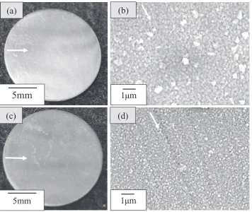
3.1 Surface morphology of samples by SEM and AFM Figure 1(b) and (d) are SEM images for samples in Fig. 1(a) and (c), before and after thermal cycle test. A rain-bow color depending on the difference of thickness by oxide layers could be seen on the surface of each sample. White arrows in Fig. 1 correspond to the direction of gas flow in MOCVD process. White particles in Fig. 1(b) and (d) are crystalline of Er2O3 according to our recent work4), and its mean size is about 170 nm in Fig. 1(b), while the mean size of particle after thermal test was smaller value of about 130 nm in Fig. (d). Figure 1(b) also shows some coarser par-ticles, which are probably contamination during MOCVD process or aggregation of small particles around 170 nm in diameter. The mean size of 170 nm in the present work was remarkably smaller than Er2O3 thin film without buffer layer
reported by the previous our report. Figure 2(a) and (b) shows AFM images for samples before and after thermal cy-cle test. Mean distance between peaks were measured as 200 nm and 140 nm. Those values are also similar to the mean size of particles on SEM images in Fig. 1(b) and (d). Figure 3 shows XRD profiles for each sample before and af-ter thermal cycle test. Peaks of Er2O3 and Y2O3 crystalline were detected for each sample, because the crystal structure of each oxide is the same as C-rare earth structure (space group: Ia3)3) and their lattice parameters are similar to each other. And each crystalline is preferentially oriented to (222)Er2O3 and (222)Y2O3.
3.2 Er2O3 and Y2O3 buffers before thermal cycling test Figure 4 (a) shows a X-TEM bright field images of Er2O3 thin film with Y2O3 buffer before thermal cycle prepared by FIB method. The Er2O3 thin film has columnar structure and it is about 620 nm for thickness before thermal cycling. Also the Y2O3 thin film has the narrower columnar structure about 690 nm for thickness than Er2O3 thin film. The difference of the cross-sectional images between two thin films was the difference of coating methods which means MOCVD for Er2O3 and PVD for Y2O3. The selected area electron diffrac-tion (SAED) patterns were obtained from the parts of Er2O3 thin film and Y2O3 buffer layers as Fig. 4 (b) and (c), and these incident electron beam directions were indexed as
<110>Er2O3 and <110>Y2O3, respectively. <111>Er2O3 and <111>Y2O3 are mostly parallel to growth directions of each layer, although it has a deviation about 6–8 degrees. The sample was made the hole as Fig. 4 (a) using FIB technique Fig. 1 Overviews((a), (c)) and SEM images ((b), (d)) of samples. (a) and (b) Er2O3/Y2O3 before thermal cycle, (c) and (d) Er2O3/Y2O3 after 30 thermal
[image:2.595.123.480.72.372.2]by low Ga+ ion beam to obtain HRTEM image from Er 2O3 thin film and Y2O3 buffer layer, respectively.
Figure 5 (a) and (c) were HRTEM images obtained for Er2O3 thin film and Y2O3 layer around the hole at points A and B in Fig. 4 (a), respectively. Figure 5 (b) and (d) were the enlarged images processed for white squares in Fig. 5 (a) and (c), and show 2 lattice spacings of about 0.30 and 0.26 nm. Those lattice spacings correspond to spacings of
[image:3.595.86.513.72.248.2]{222} Er2O3/Y2O3 and {400} Er2O3/Y2O3, respectively. The direction of white arrows in Fig. 5(a) and (c) are in good agreement with <111>Er2O3 and <111>Y2O3, and those di-rections also correspond to growth didi-rections of Er2O3 and Y2O3 crystalline. This result also supports to the XRD anal-ysis in Fig. 3.
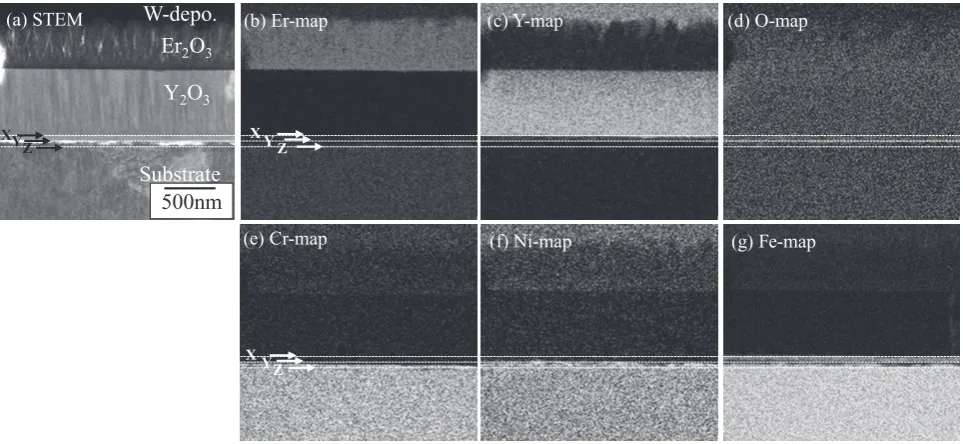
Figure 6 shows STEM images obtained for the same sam-ple as Fig. 4 and STEM-EDS maps. Er, Y, O, Cr, Ni and Fe show homogenous distribution of these elements in each layer. It is noted that two extra layers between Y2O3 and SUS316 substrate can be seen in Fig. 6(a). Lines X, Y and Z were drown in Fig. 6. There are light gray layer between lines X and Y, and brighter layer between Y and Z. According to EDS maps, Er and Y distribute upto the line Y. On the other hand, Fe achieved to the line X, and Cr and O to the line Y. This means that light gray layer between X and Y probably consist of Er, Y, Fe and O, and brighter layer be-tween Y and Z consist of Cr, Ni and O. Those layers are maybe complex oxides which were formed during heating of MOCVD.
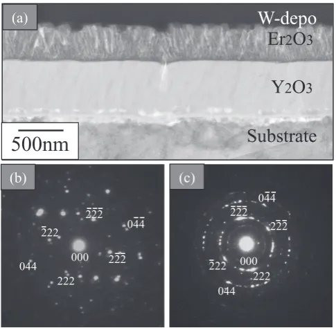
3.3 Effect of thermal cycles on Er2O3 film with buffer As-deposited sample was provided for the thermal cycling test which is 30 times of heating-cooling sequence from room temperature to about 1023 K. Figure 7 (a) shows a X-TEM bright field image of Er2O3 thin film with Y2O3 buf-fer after 30 thermal cycles prepared by FIB method. The Er2O3 thin film has columnar structure and about 390 nm for thickness after thermal cycling, and the thickness decreased remarkably without any other damages, for example, crack-ing and some pores, cavities by diffusion. Y2O3 buffer layer had been maintained for columnar structure and the thick-ness during the heat cycles. SAED patterns were obtained Fig. 2 AFM images obtained for each sample surface. (a) Er2O3/Y2O3 before thermal cycle, and (b) Er2O3/Y2O3 after 30 thermal cycles.
Fig. 3 XRD profiles obtained for (a) Er2O3/Y2O3 before thermal cycle,
and (b) Er2O3/Y2O3 after 30 thermal cycles.
Fig. 4 TEM images obtained for the X-TEM sample of Er2O3/Y2O3
be-fore thermal cycle. (a) a bright field image of whole area of this sample, and SAED patterns obtained for (b) Er2O3 layer and (c)Y2O3 layer,
respectively.
[image:3.595.63.279.299.440.2] [image:3.595.49.290.498.715.2]Fig. 5 (a) and (c) HRTEM images obtained for Er2O3 and Y2O3 layers. (b) and (d) enlarged images processed for regions marked by white squares in (a)
and (c), respectively. Solid lines in Fig. 5 (b) and (d) indicate the lattice planes of {222} Er2O3/Y2O3 and {400} Er2O3/Y2O3, respectively.
[image:4.595.125.476.72.414.2] [image:4.595.58.540.488.710.2]for parts of Er2O3 thin film and Y2O3 buffer layer as Fig. 7 (b) and (c), and each incident electron beam direction was indexed as <110>Er2O3 and <110>Y2O3. <111>Er2O3 and <111>Y2O3 are mostly parallel to growth directions of each layer, although it has a deviation about 6–8 degrees. It is also the same as the result of samples without thermal cycle in Fig. 4. It means that the orientation relationship and growth direction between Er2O3 thin film and Y2O3 layer hadn t change during thermal cycles because of similarity of crystal structure and good adhesion between Er2O3 and Y2O3
layers.
Figure 8 shows that STEM image and STEM-EDS maps obtained for same sample of Fig. 7 (a). According to these maps of Fig 8, Fe, Cr, and Ni have not been detected from Er2O3 and Y2O3 layers, and these elements had not been dif-fused into each film during thermal cycling. Figure 8 (h) is enlarged image marked by a black rectangular in Fig. 8 (a). White dashed lines in this figure indicate the same positions at the interface. It was noted that an unknown bright region marked by an arrow, which is isolated and more grown than that in Fig. 6, exists between Y2O3 buffer layer and SUS316 substrate after thermal cycles. Oxygen rich layer in Fig. 8 (d) and Fe rich part in Fig. 8 (g) were corresponded to the bright region between Y2O3 and SUS316 substrate in Fig. 8 (h). It is suggested that complex oxides would be grown to particle shape from a thin layer during thermal cycles with-out extra diffusion from Er2O3 or Y2O3 layers. <111>Er2O3 and <111>Y2O3 are mostly parallel to growth directions of each layer, although they have a deviation about 6–8 degrees according to Figs. 4 and 7. For accurate analysis for SAED pattern in Fig. 4, however, the correct growth direction for Er2O3 and Y2O3 were <133>Er2O3 and <111>Y2O3, not per-fect <111>Er2O3 and <111>Y2O3 on cube-cube relationship. <133>Er2O3 and <111>Er2O3 makes an angle of 12 degrees. As there is angular deviation for growth direction of Er2O3 because of fluctuation of gas flow during MOCVD process, which is the same as the previous report4), we assumed that the growth direction of Er2O3 column in the present work is mostly equal to the cube-cube orientation relationship. The best orientation relationship for misfit is 0.51% between
{001}Er2O3 and {001}Y2O3 of the cube-cube relationship ac-cording to the eq. (1), when the lattice parameters of 1.0548 nm and 1.0602 nm were used for Er2O3 and Y2O3 to each other9).
Fig. 7 TEM images obtained for the X-TEM sample of Er2O3/Y2O3 after
thermal cycle. (a) a bright field image of whole area of this sample, and SAED patterns obtained for (b) Er2O3 layer and (c)Y2O3 layer,
respectively.
Fig. 8 (a) STEM bright field image of the sample after thermal cycles and EDS maps obtained the same area as (a). (b) Er, (c) Y, (d) O, (e) Cr, (f) Ni and (g) Fe maps. (h) an enlarged image marked by a black dashed rectangular in (a). White dashed lines indicate the same positions of interface.
[image:5.595.49.292.217.454.2] [image:5.595.57.539.521.761.2]mis f it(hkl)Er2O3
(hkl)Y2O3[%]
= d(hkl)Er2O3−d(hkl)Y2O3
d(hkl)Er2O3 ×100 (1) It is also suggested that the thermal cycling test do not give any effect for orientation relationship for the growth direc-tions both of Er2O3 and Y2O3 layers.
4. Conclusions
Morphology and microstructure of Er2O3 thin film fabri-cated by MOCVD method on the SUS316 substrates with and Y2O3 buffer layer fabricated by RF-sputtering were in-vestigated by some electron microscopes, XRD and AFM before and after thermal cycling test.
(1) The surface morphology of Er2O3 thin film was granu-lar structure with a size of about 170–200 nm in diameter before thermal cycling test, and then it was decreased to 130–140 nm after thermal cycling test using by SEM and AFM observation.
(2) XRD peaks of Er2O3 and Y2O3 were detected for each sample before and after thermal cycles. The crystalline is preferentially oriented to (222)Er2O3 and (222)Y2O3.
(3) The microstructure of Er2O3 thin film with Y2O3 buffer layer had not be seen any distinct damages before and after thermal cycling, although the thickness of Er2O3 thin film decreased from about 620 nm to about 390 nm. Fe, Cr and Ni elements in SUS316 substrate were not detected in each Er2O3 or Y2O3 layer.
(4) The results obtained for SAED and XRD analysis re-vealed that orientation relationship of the growth direction
for Er2O3 and Y2O3 layers had not been changed during ther-mal cycles.
Acknowledgement
This project has been supported by NIFS research founda-tion 2016, and President descripfounda-tion, University of Toyama 2016.
REFERENCES
1) B.A. Pint, P.F. Tortorelli, A. Jankowski, J. Hayes, T. Muroga, A. Suzuki, O.I. Yeliseyeva and V.M. Chernov: J. Nucl. Mater. 329–333 (2004) 119–124.
2) M. Tanaka, M. Takezawa, Y. Hishinuma, T. Tanaka, T. Muroga, S. Ikeno, S. Lee and K. Matsuda: Plasma & Fusion Res. 11 (2016) 2405120-1–2405120-3.
3) Y. Hishinuma, S. Murakami, K. Matsuda, T. Tanaka, Y. Tasaki, T. Tanaka, T. Nagasaka, A. Sagara and T. Muroga: Plasma & Fusion Res. 7 (2012) 2405127-1–0405127-4.
4) T. Shinkawa, K. Matsuda, Y. Hishinuma, K. Nishimura, T. Tanaka, T. Muroga and T. Sato: Mater. Trans. 55 (2014) 1781–1785.
5) S. Lee, T. Shinkawa, K. Matsuda, M. Tanaka, Y. Hishinuma, K. Nishimura, T. Tanaka, T. Tanaka, T. Muroga and T. Sato: Mater. Trans. 58 (2017) 231–235.
6) H. Zhang, J. Yang, H. Liu and S. Wang: Physica C 470 (2010) 1998–2001.
7) Y. Hishinuma, T. Tanaka, T. Shinkawa, S. Murakami, K. Matsuda, T. Watanabe, T. Nagasaka, A. Sagara and T. Muroga: Fus. Sci. Technol. 66 (2014) 221–227.
8) Y. Hishinuma, T. Tanaka, T. Tanaka, T. Nagasaka, T. Tasaki, S. Murakami, K. Matsuda, A. Sagara and T. Muroga: Fus. Sci. Technol. 60 (2011) 1131–1134.