Solid-State Reactive Diffusion between Sn and Electroless Ni–P at 473 K
Masafumi Yamakami
1and Masanori Kajihara
2;*1Graduate School, Tokyo Institute of Technology, Yokohama 226-8502, Japan
2Department of Materials Science and Engineering, Tokyo Institute of Technology, Yokohama 226-8502, Japan
Nickel–phosphorus alloys are electrolessly deposited onto Cu-base conductors to suppress formation of Cu–Sn compounds during soldering using Sn-base solders. However, a Ni–Sn compound is produced during soldering, and continuously grows during energization heating at solid-state temperatures. To examine influence of P on the growth behavior of the Ni–Sn compound during energization heating, the kinetics of the solid-state reactive diffusion between Sn and electroless Ni–P alloys was experimentally determined at 473 K in the present study. For the experiment, pure Cu sheets were electrolessly deposited with Ni–P alloys containing 4.6 at%, 18.5 at% and 20.4 at% of P, and then sandwiched between pure Sn plates. Such Sn/(Ni–P)/Cu/(Ni–P)/Sn diffusion couples were isothermally annealed at 473 K for various periods up to 1307 h. During annealing, a layer of Ni3Sn4is formed along the Sn/(Ni–P) interface in the diffusion couple. The annealing time dependence of the mean thickness of the Ni3Sn4 layer is expressed by a parabolic relationship. The parabolic coefficient slightly increases with increasing P concentration in the Ni–P. Thus, P in the Ni–P lightly accelerates the growth of Ni3Sn4at the interconnection between the Ni–P and the Sn-base solder. Using the experimentally determined values of the parabolic coefficient, the interdiffusion coefficient in Ni3Sn4 was analytically evaluated by a mathematical model. The acceleration effect of P on the growth of Ni3Sn4is quantitatively explained by the dependence of the interdiffusion coefficient on the P concentration in the Ni–P. [doi:10.2320/matertrans.MRA2008266]
(Received August 11, 2008; Accepted October 27, 2008; Published December 17, 2008)
Keywords: diffusion bonding, reactive diffusion, intermetallic compounds, bulk diffusion, solder, conductor, electroless deposition
1. Introduction
In the electronics industry, Cu-base alloys are widely used as conductor materials. However, Cu is not completely corrosion resistant. Hence, the Cu-base alloy is usually plated with a Au layer to improve corrosion resistance. If the Au/Cu conductor material is interconnected using a Sn-base solder, the Au layer may quickly dissolve into the molten Sn-base solder during soldering unless the Au layer is sufficiently thick. When the Au layer dissolves, Cu–Sn compounds are formed at the interconnection due to the reactive diffusion between the Cu-base alloy and the molten Sn-base solder. Since the Cu–Sn compounds are brittle and possess high electrical resistivities, their formation deteriorates the elec-trical and mechanical properties of the interconnection. The formation behavior of the Cu–Sn compounds has been experimentally studied by many investigators.1–17) To
sup-press Cu–Sn compounds formation during soldering, the Cu-base alloy is generally plated with a Ni layer prior to Au layer deposition. In such a multilayer Au/Ni/Cu conductor material, the Ni layer actually acts as an effective barrier against the reactive diffusion between the Sn-base solder and the Cu-base alloy.18–20)
The Ni layer electrolessly deposited onto the Cu-base alloy usually contains 5–20 at% of P. The reactive diffusion between the electroless Ni–P layer and the Sn-base solder has been experimentally studied by many researchers.20–39)
However, a soldering technique has been used in most of these studies. In this technique, a diffusion couple is prepared from a molten Sn-base solder and a (Ni–P)/Cu conductor material at soldering temperatures, and then isothermally annealed at solid-state temperatures. Compound layers with certain thicknesses are formed during soldering, and con-tinously grow during annealing. Therefore, it is not so easy to distinguish the growth rate during annealing from the formation rate during soldering. Consequently, the soldering
technique may not be adequate to observe the growth behavior of the compound layers due to annealing at solid-state temperatures.
On the other hand, a diffusion bonding technique has been used to examine experimentally the solid-state reactive diffusion in many alloy systems in previous studies.40–61)In this technique, a diffusion couple is prepared from different metals or alloys by isothermal heating at the same temper-ature as isothermal annealing. Hence, the growth behavior of compound layers during heating and annealing at a constant temperature can be readily observed by the diffusion bonding technique. Although Ni is an effective barrier to suppress the Cu–Sn compounds formation, addition of P to Ni may degrade the effect of Ni.20)However, there is hardly reliable
information for such influence of P. To examine influence of P on the effect of Ni, the solid-state reactive diffusion between Sn and electroless Ni–P alloys with different com-positions was experimentally determined by the diffusion bonding technique in the present study. The mathematical model reported in a previous study62) was used to analyze quantitatively the experimentally observed kinetics of the reactive diffusion.
2. Experimental
Polycrystalline plate specimens of pure Sn with a size of
12mm5mm2mm were prepared by cold rolling and spark erosion from a commercial 1 kg rectangular ingot of pure Sn with purity of 99.99%. The cold-rolled plate specimens were separately annealed in evacuated silica capsules at 473 K for 2 h, followed by air cooling without breaking the capsules. The annealed Sn plate specimens were chemically polished in an etchant consisting of 20 vol% of nitric acid, 20 vol% of hydrochloric acid and 60 vol% of distilled water. The two surfaces with an area of 12mm
5mm of each Sn plate specimen were mechanically polished on 800 emery paper. One of the two polished surfaces was again mechanically polished on 1000–4000 emery papers
until a depth of 100mmand then finished using diamond with a diameter of 1mm.
Polycrystalline Cu sheet specimens with a thickness of 50mm and purity of 99.99% were electrolessly deposited with Ni–P layers with various compositions. Such (Ni–P)/ Cu/(Ni–P) sheet specimens were supplied by Japan Kanigen Co. Ltd. The chemical composition and the initial thickness of the electroless Ni–P layer are listed in Table 1. In this table, the composition is shown as the mol fraction yof P. The Ni–P layers withy¼0:045{0:047,y¼0:181{0:190and
y¼0:204{0:205are denominated layers A1–A3, B1–B2 and C1–C3, respectively, and the mean of yis equal to 0.046, 0.185 and 0.204 for layers A1–A3, B1–B2 and C1–C3, respectively. Sheets with an area of12mm5mm were cut from the (Ni–P)/Cu/(Ni–P) specimen, and then degreased with acetone in an ultrasonic cleaning equipment. The crystal structure of the Ni–P layer was determined by an X-ray diffraction (XRD) technique using Cu Kradiation.
After degreasing, a (Ni–P)/Cu/(Ni–P) sheet specimen was immediately sandwiched between the finished surfaces of two freshly prepared Sn plate specimens in ethanol by a technique used in a previous study.19) The Sn/(Ni–P)/Cu/
(Ni–P)/Sn couples were completely dried and then heat treated for diffusion bonding in an oil bath with silicone oil at 473 K for 24 h. After the heat treatment, the diffusion couples were isothermally annealed at 473 K for various times up to 1283 h. The summation of the heat-treating and annealing times is hereafter merely called the annealing timet. Cross-sections of the annealed diffusion couples were mechanically polished using diamond with diameters of 15, 3 and 1mmand then finished with an OP-S liquid by Struers Ltd. The microstructure of the cross-section was observed with an optical microscope (OM). The composition of each phase was measured on the cross-section by electron probe micro-analysis (EPMA).
3. Results and Discussion
3.1 X-ray diffraction measurement
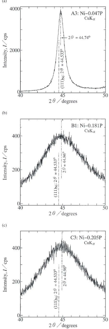
Typical XRD patters are shown in Fig. 1. Figure 1(a), (b) and (c) indicates the results of layers A3, B1 and C3, respectively. As can be seen, a sharp diffraction peak is observed at2¼44:74 for layer A3, and broad diffraction
peaks are recognized at2¼44:86and 44.90for layers B1 and C3, respectively. Since the lattice parameter of Ni is
aNi¼0:35238nm and the wavelength of Cu K X-ray is
(b)
(c)
[image:2.595.312.539.78.758.2] [image:2.595.46.291.95.220.2]¼0:154178nm,63)the diffraction peak for the (111) plane
of Ni will appear at2¼44:533according to the following
relationship.
2dsin¼ ð1Þ
Here, the lattice spacing for the (111) plane of Ni is
dNi¼0:20345nm. As a consequence, layer A3 is a
crystal-line phase with the face-centered cubic (fcc) structure, but layers B1 and C3 are amorphous. The XRD measurements of all the Ni–P layers are summarized at the fifth column in Table 1. The crystal structure of electroless Ni–P was experimentally observed in the composition range of y¼
0:055{0:236 by Kumar and Nair,64) Gao et al.,65) and
Palaniappa and Seshadri.66)According to their observations,
the electroless Ni–P is the fcc phase for y¼0:055{0:079, a mixture of the fcc and amorphous phases for y¼
0:079{0:159, and amorphous for y¼0:159{0:236. The result in Table 1 is consistent with their observations.
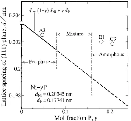
Using the values of2for the sharp and broad diffraction peaks in Fig. 1, the lattice spacingd of the (111) plane was evaluated from eq. (1). Unlike layer A3, however, layers B1 and C3 are amorphous. In the case of the amorphous layer,d
corresponds to the mean lattice spacing of the closed-pack plane. The evaluated values ofdare plotted against the mol fractionyof P as open circles in Fig. 2. In this figure, an open square shows the corresponding value of Ni. As can be seen,
d is smaller for layers A3, B1 and C3 than for Ni. Thus, addition of P to Ni decreases the interatomic distance. According to Vegard’s law,d may be expressed as a linear function ofyby the equation
d¼ ð1yÞdNiþy dP; ð2Þ
where dP is the lattice spacing of the (111) plane for a
hypothetical fcc-phase of P. Combining dNi¼0:20345nm
with the atomic radiirNi¼0:125nm andrP¼0:109nm of
Ni and P, respectively,63)we obtaindP¼0:17741nm. Using
these values of dNi and dP, the dependence of d on y was
calculated from eq. (2). The result is shown as a bold straight
line in Fig. 2. On the other hand, vertical thin dashed-and-dotted lines indicate the critical compositionsy¼0:079and 0.159. As can be seen, the open circle of layer A3 withy¼
0:047lies well on the bold straight line. According to a recent phase diagram in the binary Ni–P system,67)the two-phase
microstructure consisting of the fcc Ni phase and Ni3P is
stable for y¼0:00045{0:25 at room temperature. Further-more, the solubility of P in the Ni phase is merelyy¼0:0032
even at 1143 K. Nevertheless, any diffraction peaks of Ni3P
were not observed in all the XRD measurements. As mentioned above, the open circle of layer A3 almost obeys eq. (2). Thus, it is concluded that the electroless Ni–P with
y¼0:05is the fcc Ni phase supersaturated with P and the Ni atoms in the fcc lattice are substitutionally replaced with P atoms. In contrast, the open circles of layers B1 and C3 are located on the upper side of the bold straight line. Hence, eq. (2) is not valid for the amorphous phase in the binary Ni–P system.
3.2 Microstructure
A typical micrograph of OM for the cross-section of the annealed diffusion couple is shown in Fig. 3. This figure indicates the micrograph for the diffusion couple with layer A1 annealed at 473 K for 309 h (1.11 Ms). In Fig. 3, the regions on the upper and lower sides are the Sn specimen, the horizontal band with a thickness of about 50mm is the Cu specimen, and the gray layers with a uniform thickness adjacent to the Cu are the electroless Ni–P. As can be seen, a rather wavy compound layer is formed at each interface between the Ni–P and Sn. This compound layer is Ni3Sn4.
Concentration profiles of Ni, Sn and P across the Ni3Sn4and
Ni–P layers were determined by EPMA. The results of the diffusion couples with layers A3, B1 and C1 annealed at 473 K for 1307 h (4.71 Ms) are shown as open symbols in Fig. 4(a), (b) and (c), respectively. Hereafter, the diffusion couples with layers A1–A3, B1–B2 and C1–C3 are merely called diffusion couples A1–A3, B1–B2 and C1–C3, respec-tively. In Fig. 4, the abscissa indicates the distancex, and the ordinate shows the mol fractionyi of componenti (i¼Ni,
Sn, P). As can be seen, the mol fractionyPof P is negligible in
the Sn, Cu and Ni3Sn4. On the other hand, in the Ni–P layer,
Fig. 2 The lattice spacingdof the (111) or closed-pack plane versus the mol fractionyof P for layers A3, B1 and C3 shown as open circles. The bold straight line indicates Vegard’s law.
[image:3.595.312.540.69.247.2] [image:3.595.62.280.71.273.2]yPis greater after annealing than before annealing. Hereafter,
the values ofyPin the Ni–P layer before and after annealing
are denoted by yand yNiP
P , respectively. The concentration
profiles in Fig. 4 are plotted as diffusion paths in Fig. 5. In this figure, the ordinate and the abscissa show ySn and yP,
respectively, and open triangles, rhombuses and circles indicate the results of diffusion couples A3, B1 and C1, respectively. In contrast, open squares show y. SinceyP in
Ni3Sn4 is negligible, P atoms are excluded from Ni3Sn4 to
the Ni–P layer due to growth of Ni3Sn4. Consequently,yNiPP
gradually increases with increasing annealing time. As can be seen in Fig. 4, the maximum value of yNiP
P at an annealing
time of t¼1307h (4.71 Ms) is 0.064, 0.243 and 0.253 for diffusion couples A3, B1 and C1, respectively. The mol fractionyNi3P
P of P in Ni3P is equal to 0.25. The valuesyNiPP ¼ 0:243and 0.253 are close toyNi3P
P ¼0:25.
In the binary Ni–Sn system,68)Ni
3Sn2and Ni3Sn as well as
Ni3Sn4 appear as stable compounds at 473 K. On the other
hand, P3Sn, P4Sn3 and P3Sn4 are the stable compounds at
473 K in the binary P–Sn system.69) Nevertheless, only Ni3Sn4 was observed as a Sn-base compound under the
present annealing conditions. The solid-state reactive diffu-sion between Sn and an electroless Ni–P layer withy¼0:174
was experimentally studied by Tomlinson and Rhodes.20)In their experiment, a Ni–P layer with a thickness of 20mmwas deposited onto a mild steel substrate, and then a pure Sn layer with a thickness of 20mmwas deposited onto the Ni–P layer. Although the thickness of the Ni–P layer is not so different between their study and the present study, the thickness of the Sn layer is two orders of magnitude smaller in their study than in the present study. Such multilayer Sn/(Ni–P)/steel diffusion couples were isothermally annealed in the temper-ature range between 453 and 493 K for various times up to 508 h. Also in their experiment, a Ni3Sn4layer was observed
at the Sn/(Ni–P) interface in the annealed diffusion couple. Furthermore, the enrichment of P was observed in the Ni–P layer after annealing. Unfortunately, however, the concen-tration change of P in the Ni–P layer was not quantitatively determined in their experiment.
(b)
(c)
Fig. 4 Concentration profiles of Ni, Sn and P across the Ni3Sn4and Ni–P layers after annealing at 473 K for 1307 h: (a) diffusion couple A3, (b) diffusion couple B1 and (c) diffusion couple C1.
[image:4.595.65.273.68.764.2] [image:4.595.324.528.74.273.2]3.3 Growth behavior of Ni3Sn4
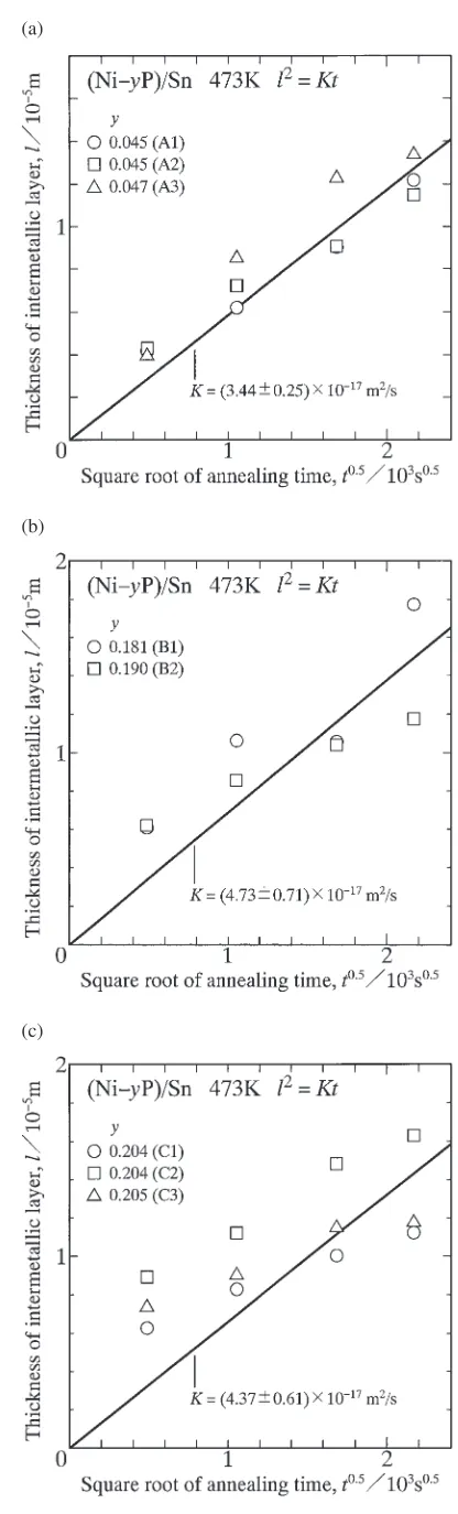
From cross-sectional OM micrographs like Fig. 3, the mean thickness lof the Ni3Sn4 layer was evaluated by the
equation
l¼A=w; ð3Þ
whereAandware the area and the length of the Ni3Sn4layer,
respectively, on the cross-section. Hereafter, the Ni3Sn4layer
is merely called the intermetallic layer. At each annealing time,lwas calculated from eq. (3) using the total values ofA
and w for various cross-sections. The results of diffusion couples A1–A3, B1–B2 and C1–C3 are shown as open symbols in Fig. 6(a), (b) and (c), respectively. In this figure, the ordinate indicates the thicknessl, and the abscissa shows the square root of the annealing time t. Although the open symbols are slightly scattered, we may expect that l is proportional to the square root of t. Such a relationship is called the parabolic relationship. The parabolic relationship is expressed by the following equation:
l2¼Kt: ð4Þ
Here,Kis the parabolic coefficient. From the open symbols in Fig. 6,Kwas evaluated by the least-squares method. In the evaluation, a common value ofKwas adopted for each mean ofy. The mean ofyis listed at the third column in Table 1. Using the evaluated values of K, l was calculated as a function oftfrom eq. (4). The results are shown as solid lines in Fig. 6. On the other hand,Kis plotted against the mean of
y as open circles with error bars in Fig. 7. In a similar manner, K was evaluated for y¼0 using the experimental data reported in a previous study.19)The result is shown as an
open square with an error bar in Fig. 7. As can be seen, K
slightly increases with increasing value ofy. This means that the growth of Ni3Sn4 is lightly accelerated by P in the
electroless Ni–P.
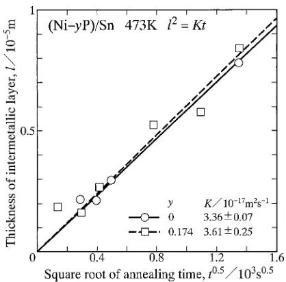
The growth behavior of Ni3Sn4 during the solid-state
reactive diffusion between Sn and Ni–P alloys withy¼0and 0.174 was experimentally studied at 453–493 K by Tomlin-son and Rhodes.20)Their results fory¼0and 0.174 at 473 K
are shown as open circles and squares, respectively, in Fig. 8. In this figure, like Fig. 6, the ordinate and the abscissa indicate the thickness l of the intermetallic layer and the square root of the annealing time t, respectively. As can be seen, the parabolic relationship holds betweenlandt, though the open symbols are slightly scattered. From the open symbols in Fig. 8, K was evaluated by the least-squares method. The evaluated values ofK are plotted against yas open rhombuses with error bars in Fig. 7. At y¼0, K is similar in the open rhombus and square. On the other hand,K
is lightly smaller for the open rhombus aty¼0:174than for the open circles at y¼0:185 and 0.204. Nevertheless, the open rhombuses also indicate thatK slightly increases with increasing value ofy.
As previously mentioned, the reactive diffusion between the Sn-base solder and the electroless Ni–P has been experimentally studied by many investigators.20–39) Accord-ing to these studies, the enrichment of P in the Ni–P occurs owing to growth of Ni3Sn4 and causes formation of Ni3P in
the Ni–P adjacent to Ni3Sn4. In the case of the experiment by
Li et al.,37)diffusion couples composed of electroless Ni–P
(a)
(b)
(c)
[image:5.595.319.527.68.755.2]alloys with P concentrations of 15–18 at% and a Sn–Bi solder with a Bi concentration of 58 at% were prepared by soldering at 493 K for 300 s, and then isothermally annealed at 473 K for various periods up to 48 h. During soldering, a Ni3Sn4
layer with a thickness of 0.93mm is formed at the (Ni–P)/ (Sn–Bi) interface, and a Ni3P layer with a thickness of
0.29mm is produced at the (Ni–P)/Ni3Sn4 interface. The
thickness l of the Ni3P layer increases to 1.25, 1.72 and
1.96mmdue to annealing for 16, 24 and 48 h, respectively. Thus, the Ni3P layer grows by l¼0:96, 1.43 and 1.67mm
owing to annealing fort¼57:6, 86.4 and 172.8 ks (16, 24 and 48 h), respectively. Using these values of l and t, the parabolic coefficient for the growth of the Ni3P layer at 473 K
is evaluated to be K¼1:751017m2/s by the least-squares method. The valueK¼1:751017m2/s results in
previous study. If a semi-infinite diffusion couple com-posed of the and phases is isothermally annealed at an appropriate temperature, a layer of the phase with a uniform thickness will be formed at the flat/interface and then grows continuously. In such a case, the interdiffusion of components A and B takes place along the direction perpendicular to the/and/ interfaces. This direction is called the diffusional direction. For the growth of the
phase controlled by volume diffusion, the distanceszand z of the/and/interfaces are expressed as functions
of the annealing timetby
z¼Kpffiffiffiffiffiffiffiffi4Dt ð5aÞ
and
z ¼Kpffiffiffiffiffiffiffiffi4Dt; ð5bÞ
respectively. Here,Dis the interdiffusion coefficient of the
phase,K andK are dimensionless coefficients, andz
and z are measured from the initial position of the /
interface along the diffusional direction. Since the thicknessl
of thephase is equal to the difference betweenzandz,
the following relationship holds betweenlandt.
l2¼ ðzzÞ2¼4DðKKÞ2t ð6Þ
Comparing eq. (6) with eq. (4), we obtain the relationship
K¼4DðKKÞ2¼ fD: ð7Þ
Here, the dimensionless factor f is defined as
f 4ðKKÞ2: ð8Þ
As reported in a previous study,62)fis a function of the initial compositions of theand phases, the compositions of the
/and/interfaces, and the interdiffusion coefficients of the , and phases. If all the independent variables of f
except the interdiffusion coefficient D of the phase are known, Dis evaluated from eq. (7) using an experimental value ofK. Such evaluation was conducted using the values of K for y¼0, 0.046, 0.185 and 0.204 by the analytical method proposed in previous studies62,70–76)according to the
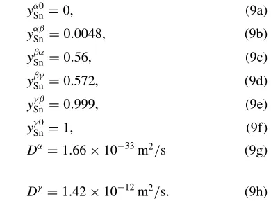
following assumptions: (1) local equilibrium is realized at each interface; (2) the interdiffusion coefficient of each phase is independent of the composition; and (3) the molar volume is constant and equivalent among all the phases. In the evaluation ofDfory¼0, the valueK¼3:411017m2/s was combined with the following parameters63,68) of the binary Ni–Sn system at 473 K:
Fig. 8 The mean thicknesslof the Ni3Sn4layer versus the annealing timet by Tomlinson and Rhodes20)at 473 K fory¼0and 0.174 shown as open circles and squares, respectively.
[image:6.595.68.275.71.275.2] [image:6.595.65.274.347.553.2]ySn0¼0; ð9aÞ
ySn ¼0:0048; ð9bÞ
ySn ¼0:56; ð9cÞ
ySn ¼0:572; ð9dÞ
ySn ¼0:999; ð9eÞ
ySn0¼1; ð9fÞ
D¼1:661033m2/s ð9gÞ
and
D ¼1:421012m2/s: ð9hÞ
Here,andstand for the Ni and Sn solid-solution phases, respectively, is Ni3Sn4,ySn0 is the initial value of the mol
fraction of Sn in thephase,ySnandySnare the mol fractions of Sn on theandsides, respectively, of the/interface,
Dis the interdiffusion coefficient of thephase (,¼, , ). The evaluation provides f ¼4:26102 and thus
D¼8:011016m2/s. As to diffusion couples A1–A3, B1–
B2 and C1–C3, the concentrations of P in theandphases are negligible as shown in Figs. 4 and 5. Hence, theand
phases are considered as the binary Ni–Sn phases. Further-more, the solubility ySn of Sn in the Ni–P (phase) is very small. For such small values ofySn, f is insensitive toySn.62)
Consequently, eq. (9a)–(9f) and (9h) is applicable to the evaluation ofDfory¼0:046{0:204. In contrast, the Ni–P is transformed into Ni3P due to exclusion of P atoms from
Ni3Sn4to the Ni–P in diffusion couples B1–B2 and C1–C3 in
the late stages of annealing. SinceDis dissimilar in Ni, Ni3P
and the Ni–P, eq. (9g) is not valid for thephase in diffusion couples A1–A3, B1–B2 and C1–C3. Even in such a case,D
may be much smaller thanD. For such small values ofD, f
is insensitive to D.62) As a result, we can use f ¼4:26 102 in the evaluation ofDalso for y¼0:046{0:204. The
[image:7.595.320.523.70.256.2]evaluated values ofDare plotted againstyas open circles in Fig. 9. As can be seen,Dslightly increases with increasing value ofy.
In a previous study,19)the growth behavior of the Ni 3Sn4
layer was originally described by the following equation but not by eq. (4).
l¼kðt=t0Þn ð10Þ
Here,kis the proportionality coefficient possessing the same dimension as l,n is the exponent, and t0 is unit time, 1 s.
According to the result in a previous study,19)nis equal to
0.459 and 0.405 at 453 K and 473 K, respectively, and thus slightly smaller than 0.5. The values of n smaller than 0.5 indicate that both boundary and volume diffusion contributes to the layer growth of Ni3Sn4 and grain growth occurs in
Ni3Sn4. If the layer growth of Ni3Sn4 is controlled by
boundary and volume diffusion, eq. (4) is no longer valid. However, the open symbols in Fig. 6 are rather scattered. Hence, unlike a previous study,19)the exponentncould not be
reliably determined by the least-squares method using the open symbols in Fig. 6. Considering the valuen¼0:405for
y¼0, we anticipate thatnis slightly smaller than 0.5 also for
y¼0:046{0:204. Thus, fory¼0{0:204, it is plausible that boundary and volume diffusion contributes to the layer growth of Ni3Sn4and the grain growth of Ni3Sn4takes place
at certain rates. In a previous study,77)the growth behavior
of a polycrystalline compound layer during the solid-state reactive diffusion controlled by boundary and volume diffusion was numerically analyzed for the same hypothetical binary A–B system as the theoretical analysis reported in a previous study.62)According to the numerical analysis, the
effective diffusion coefficient of the compound layer in-creases with decreasing grain size of the compound layer. Since the concentration of P in Ni3Sn4 is negligible as
indicated in Figs. 4 and 5, the dependence ofDonyis not attributed to the influence of P on the volume diffusion in Ni3Sn4. Therefore,Dmay contain information of boundary
and volume diffusion. The dependence of Dony in Fig. 9 implies that the grain size of Ni3Sn4 at each annealing time
gradually decreases with increasing value of y. To confirm such dependence of the grain size ony, the chemical etching of Ni3Sn4 was conducted using various etchants. However,
each grain in Ni3Sn4 could not be distinguished by the
chemical etching. Consequently, the dependence of the grain size of Ni3Sn4onywas not confirmed experimentally.
4. Conclusions
The solid-state reactive diffusion in the ternary Sn/(Ni–P) system was experimentally observed using the sandwich Sn/ (Ni–P)/Cu/(Ni–P)/Sn diffusion couples. The diffusion cou-ples with mean P concentrations of 4.6 at%, 18.5 at% and 20.4 at% were prepared by the diffusion bonding technique, and then isothermally annealed at 473 K for various times up to 1307 h in the oil bath with silicone oil. Under such annealing conditions, the Ni3Sn4 layer is formed along the
Sn/(Ni–P) interface in the diffusion couple. The square of the mean thickness of the Ni3Sn4 layer is proportional to the
annealing time. This relationship is called the parabolic relationship. The parabolic coefficient lightly increases with increasing P concentration of the Ni–P. This means that P in the Ni–P slightly accelerates the growth of Ni3Sn4. Using the
mathematical model reported in a previous study,62) the interdiffusion coefficient in Ni3Sn4 was analytically
evalu-ated from the parabolic coefficient. The dependence of the interdiffusion coefficient on the P concentration of the Ni–P
[image:7.595.98.293.73.218.2]1) L. Zakraysek: Welding Res. Suppl. Nov. (1972) 536–541. 2) K. N. Tu: Acta Metall.21(1973) 347–354.
3) M. Onishi and H. Fujibuchi: Trans. Jpn. Inst. Met.16(1975) 539–548. 4) H. N. Keller: IEEE Trans. Components Hybrids Manuf. Tech.
CHMT-2 (1979) 180–195.
5) H. N. Keller and J. M. Morabito: Surf. Interface Anal.3(1981) 16–22. 6) J. O. G. Parent, D. D. L. Chung and I. M. Bernstein: J. Mater. Sci.23
(1988) 2564–2572.
7) A. J. Sunwoo, J. W. Morris, Jr. and G. K. Lucey, Jr.: Metall. Trans. A
23A(1992) 1323–1332.
8) P. T. Vianco, P. F. Hlava and A. L. Kilgo: J. Electron. Mater.23(1994) 583–594.
9) D. R. Frear and P. T. Vianco: Metall. Trans. A25A(1994) 1509–1523. 10) S. Choi, T. R. Bieler, J. P. Lucas and K. N. Subramanian: J. Electron.
Mater.28(1999) 1209–1215.
11) P. G. Kim and K. N. Tu: J. Appl. Phys.80(1996) 3822–3827. 12) A. M. Minor and J. W. Morris, Jr.: Metall. Mater. Trans. A31A(2000)
798–800.
13) J. H. Lee, J. H. Park, Y. H. Lee and Y. S. Kim: J. Mater. Res.16(2001) 1249–1251.
14) H. G. Song, J. P. Ahn, A. M. Minor and J. W. Morris, Jr.: J. Electron. Mater.30(2001) 409–414.
15) M. O. Alam and Y. C. Chan: Chem. Mater.15(2003) 4340–4342. 16) M. O. Alam and Y. C. Chan: J. Mater. Res.19(2004) 1303–1306. 17) T. Takenaka, S. Kano, M. Kajihara, N. Kurokawa and K. Sakamoto:
Mater. Sci. Eng. A396(2005) 115–123.
18) C.-M. Chen and S.-W. Chen: Acta Mater.50(2002) 2461–2469. 19) M. Mita, M. Kajihara, N. Kurokawa and K. Sakamoto: Mater. Sci. Eng.
A403(2005) 269–275.
20) W. J. Tomlinson and H. G. Rhodes: J. Mater. Sci.22(1987) 1769– 1772.
21) C.-Y. Lee and K.-L. Lin: Thin Solid Films249(1994) 201–206. 22) J. W. Jang, P. G. Kim, K. N. Tu, D. R. Frear and P. Thompson: J. Appl.
Phys.85(1999) 8456–8463.
23) M. O. Alam, Y. C. Chan and K. C. Hung: J. Electron. Mater.31(2002) 1117–1121.
24) M. O. Alam, Y. C. Chan and K. C. Hung: Microelectronics Reliability
42(2002) 1065–1073.
25) J.-W. Yoon, C.-B. Lee and S.-B. Jung: J. Electron. Mater.32(2003) 1195–1202.
26) S. J. Wang and C. Y. Liu: Scr. Mater.49(2003) 813–818.
27) M. N. Islam, Y. C. Chan, A. Sharif and M. O. Alam: Microelectronics Reliability43(2003) 2031–2037.
28) M. He, Z. Chen and G. Qi: Acta Mater.52(2004) 2047–2056. 29) J.-W. Yoon and S.-B. Jung: J. Alloy. Compd.376(2004) 105–110. 30) M. Date, K. N. Tu, T. Shoji, M. Fujiyoshi and K. Sato: J. Mater. Res.19
(2004) 2887–2896.
31) A. Sharif, Y. C. Chan, M. N. Islam and M. J. Rizvi: J. Alloy. Compd.
388(2005) 75–82.
32) A. Sharif and Y. C. Chan: J. Alloy. Compd.393(2005) 135–140. 33) D.-G. Kim, J.-W. Kim, J.-G. Lee, H. Mori, D. J. Quesnel and S.-B.
Jung: J. Alloy. Compd.395(2005) 80–87.
34) Y.-C. Lin and J.-G. Duh: Scr. Mater.54(2006) 1661–1665.
Mater. Trans.46(2005) 969–973.
45) T. Takenaka, M. Kajihara, N. Kurokawa and K. Sakamoto: Mater. Sci. Eng. A406(2005) 134–141.
46) Y. Muranishi and M. Kajihara: Mater. Sci. Eng. A404(2005) 33–41. 47) T. Takenaka and M. Kajihara: Mater. Trans.47(2006) 822–828. 48) M. Mita, K. Miura, T. Takenaka, M. Kajihara, N. Kurokawa and K.
Sakamoto: Mater. Sci. Eng. B126(2006) 37–43.
49) Y. Yato and M. Kajihara: Mater. Trans.47(2006) 2277–2284. 50) T. Takenaka, M. Kajihara, N. Kurokawa and K. Sakamoto: Mater. Sci.
Eng. A427(2006) 210–222.
51) Y. Yato and M. Kajihara: Mater. Sci. Eng. A428(2006) 276–283. 52) T. Hayase and M. Kajihara: Mater. Sci. Eng. A433(2006) 83–89. 53) Y. Tanaka, M. Kajihara and Y. Watanabe: Mater. Sci. Eng. A445–446
(2006) 355–363.
54) A. Furuto and M. Kajihara: Mater. Sci. Eng. A445–446(2006) 604– 610.
55) D. Naoi and M. Kajihara: Mater. Sci. Eng. A459(2007) 375–382. 56) S. Sasaki and M. Kajihara: Mater. Trans.48(2007) 2642–2649. 57) K. Mikami and M. Kajihara: J. Mater. Sci.42(2007) 8178–8188. 58) M. Kajihara and T. Takenaka: Mater. Sci. Forum 539–543(2007)
2473–2478.
59) M. Kajihara and T. Sakama: Proc. 13th Symp. Microjoining Assembly Tech. Electrn., Yokohama, Japan, Feb. 1–2, 2007, (Microjoining Comm., Tokyo, 2007) 187–192.
60) T. Sakama and M. Kajihara: J. Alloy. Compd. (2008), doi: 10.1016/ j.jallcom.2008.07.113, in press.
61) M. Kajihara and S. Tanaka: Proc. 14th Symp. Microjoining Assembly Tech. Electrn., Yokohama, Japan, Feb. 5–6, 2008, (Microjoining Comm., Tokyo, 2008) 95–100.
62) M. Kajihara: Acta Mater.52(2004) 1193–1200.
63) Metals Data Book, ed. Japan Institute of Metals (Maruzen, Tokyo, 1993) pp. 23–317.
64) P. S. Kumar and P. K. Nair: J. Mater. Proc. Tech.56(1996) 511–520. 65) Y. Gao, Z. J. Zheng, M. Zhu and C. P. Luo: Mater. Sci. Eng. A381
(2004) 98–103.
66) M. Palaniappa and S. K. Seshadri: Mater. Sci. Eng. A460–461(2007) 638–644.
67) T. B. Massalski, H. Okamoto, P. R. Subramanian and L. Kacprzak: Binary Alloy Phase Diagrams, vol. 3 (ASM International, Materials Park, OH, 1990) p. 2835.
68) T. B. Massalski, H. Okamoto, P. R. Subramanian and L. Kacprzak: Binary Alloy Phase Diagrams, vol. 3 (ASM International, Materials Park, OH, 1990) p. 2864.
69) T. B. Massalski, H. Okamoto, P. R. Subramanian and L. Kacprzak: Binary Alloy Phase Diagrams, vol. 3 (ASM International, Materials Park, OH, 1990) p. 2985.
70) M. Kajihara: Mater. Sci. Eng. A403(2005) 234–240. 71) M. Kajihara: Mater. Trans.46(2005) 2142–2149. 72) M. Kajihara: Def. Diff. Forum249(2006) 91–96. 73) M. Kajihara: Mater. Trans.47(2006) 1480–1484.
74) Y. Tanaka and M. Kajihara: Mater. Trans.47(2006) 2480–2488. 75) M. Kajihara and T. Yamashina: J. Mater. Sci.42(2007) 2432–2442. 76) M. Kajihara: Mater. Trans.49(2008) 715–722.