Selective modification of nanoparticle arrays by
laser-induced self assembly (MONA-LISA): putting control into
bottom-up plasmonic nanostructuring
KALFAGIANNIS, N., SIOZIOS, A., BELLAS, D.V., TOLIOPOULOS, D.,
BOWEN, L., PLIATSIKAS, N., CRANTON, W.M.
<http://orcid.org/0000-0002-0142-7810>, KOSMIDIS, C., KOUTSOGEORGIS, D.C., LIDORIKIS, E. and
PATSALAS, P.
Available from Sheffield Hallam University Research Archive (SHURA) at:
http://shura.shu.ac.uk/12469/
This document is the author deposited version. You are advised to consult the
publisher's version if you wish to cite from it.
Published version
KALFAGIANNIS, N., SIOZIOS, A., BELLAS, D.V., TOLIOPOULOS, D., BOWEN, L.,
PLIATSIKAS, N., CRANTON, W.M., KOSMIDIS, C., KOUTSOGEORGIS, D.C.,
LIDORIKIS, E. and PATSALAS, P. (2016). Selective modification of nanoparticle
arrays by laser-induced self assembly (MONA-LISA): putting control into bottom-up
plasmonic nanostructuring. Nanoscale, 8 (15), 8236-8244.
Copyright and re-use policy
See
http://shura.shu.ac.uk/information.html
PAPER
Cite this:Nanoscale, 2016,8, 8236
Received 24th December 2015, Accepted 18th March 2016 DOI: 10.1039/c5nr09192f
www.rsc.org/nanoscale
Selective modi
fi
cation of nanoparticle arrays by
laser-induced self assembly (MONA-LISA): putting
control into bottom-up plasmonic
nanostructuring
†
Nikolaos Kalfagiannis,*
aAnastasios Siozios,
bDimitris V. Bellas,
bDimosthenis Toliopoulos,
bLeon Bowen,
cNikolaos Pliatsikas,
dWayne M. Cranton,
a,eConstantinos Kosmidis,
fDemosthenes C. Koutsogeorgis,
aElefterios Lidorikis
band
Panos Patsalas
dNano-structuring of metals is one of the greatest challenges for the future of plasmonic and photonic devices. Such a technological challenge calls for the development of ultra-fast, high-throughput and low-cost fabrication techniques. Laser processing, accounts for the aforementioned properties, repre-senting an unrivalled tool towards the anticipated arrival of modules based in metallic nanostructures, with an extra advantage: the ease of scalability. In the present work we take advantage of the ability to tune the laser wavelength to either match the absorption spectral profile of the metal or to be resonant with the plasma oscillation frequency, and demonstrate the utilization of different optical absorption mechanisms that are size-selective and enable the fabrication of pre-determined patterns of metal nano-structures. Thus, we overcome the greatest challenge of Laser Induced Self Assembly by combining simultaneously large-scale character with atomic-scale precision. The proposed process can serve as a platform that will stimulate further progress towards the engineering of plasmonic devices.
Introduction
Nanomaterial and nanodevice manufacturing has traditionally followed two distinct routes: the top-down approach,1–3where physical processes such as e-beam and photo-lithography are exploited for slicing and dicing macroscopic entities in the nanoscale, and the bottom-up approach, where atomic-scale chemical forces take centre stage and drive molecular self-assembly.4–7Crudely speaking, one might say they correspond
to the competing worlds of Physics and Chemistry. In practice, the top-down route offers unparalleled control and reproduci-bility down to a few nanometres in feature size but at high cost for large area processing, while the bottom-up approach natu-rally applies for macroscopic scale nano-patterning albeit without the fine feature and reproducibility control. Laser Annealing (LA from now on) might be viewed as the means to a third, intermediate route for nanotechnology manufacturing. Light-matter interactions offer precise energy delivery and control over the physico-chemical processes in the nanoworld. It has already been implemented for the reshaping of plasmo-nic nanoparticles,8–11 alloying at the nanoscale12 and nano-manipulation in optical tweezers.13–15Today’s laser technology in nano-manufacturing, however, lacks the simultaneous atomic-scale control and large-scale character: processes can be either extremely accurate but implemented in infinitesi-mally small volumes8,13 or can be macroscopically implemented with a lesser control on the produced features.10 In this work we show that it is possible to overcome these limitations and substantially improve the control of bottom-up nano-patterning. The targeted plasmonic applications span from size- and shape-selective biocompatible surfaces,16 surface enhanced Raman scattering,17,18 optical storage of information,10 production of metal nanocavities for light
†Electronic supplementary information (ESI) available: Extensive experimental results that corroborate the results and conclusions presented in the manu-script, but due to their extent cannot fit in the manuscript. The manuscript refers to specific sections here, but in its entirety this document presents the complete results of our MONA-LISA work. See DOI: 10.1039/c5nr09192f
aNottingham Trent University, School of Science and Technology, Nottingham,
NG11 8NS, UK b
University of Ioannina, Department of Materials Science and Engineering, 45110 Ioannina, Greece
c
University of Durham, G. J. Russell Microscopy Facility, South Road, Durham, DH1 3LE, UK
dAristotle University of Thessaloniki, Department of Physics, 54124 Thessaloniki,
Greece
eSheffield Hallam University, Materials and Engineering Research Institute, Sheffield,
S11 WB, UK f
University of Ioannina, Department of Physics, 45110 Ioannina, Greece
Open Access Article. Published on 21 March 2016. Downloaded on 23/06/2016 09:41:34.
This article is licensed under a
Creative Commons Attribution 3.0 Unported Licence.
View Article Online
manipulation and enhancement of solid state lighting,19,20as well as broadband solar energy harvesting by incorporating the considered plasmonic nanoparticles into photothermal, photocatalytic and photovoltaic devices.21–24At the very heart of these applications lie the light-matter interactions, in the form of coherent surface plasmon oscillations excited by the incident light at specific frequencies with high selectivity on the metal nanostructure’s size and shape. But selective plasmon excitation translates into selective light absorption, and thus into selective heating of the nanostructure.
It is natural thus to allow this core property of the target application, to become itself one of the drivers in the self-assem-bly process. Furthermore, besides heating, selective cooling is also an integral part of restructuring. But as the cooling rate depends on the geometric features of the nanostructure, a second driver for the self-assembly process is introduced.
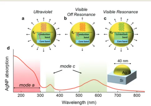
The available light absorption mechanisms in the case of nanostructured noble metals such as Ag, Au and Cu, can be intuitively summarized in the following modes:
(a) interband absorption, probing the metal’s internal d-electrons (Fig. 1a). This is typically enabled at UV frequencies and in general is not size-dependent,
(b) off-resonance intraband (free electron) absorption (Fig. 1b), which however is too weak to cause substantial temperature rise,
(c) resonant intraband absorption (Fig. 1c), probing the conduction electrons with laser wavelengths close to the spec-tral position of Localised Surface Plasmon Resonance (LSPR). This mechanism is strongly size- and shape-selective, and
(d) photon ionization that may occur only for high laser fluences.25
As an example, the overall absorption spectrum of Ag nano-particle with diameter of 40 nm on top of a Si substrate is
plotted in Fig. 1d, showing the spectral domains of the two absorption mechanisms. Hereby, we utilize modes (a) and (c), combined with the size selectivity of cooling (∼nanostructure surface/volume ratio) and demonstrate that this approach pro-vides an exceptional and versatile tool for controlling the self-assembly of nanoparticles, leading to desired nanoparticles distributions, which cannot be achieved by the exclusive use of UV laser annealing.
Experimental
Sample preparationMetallic thin films were deposited employing the following experimental techniques:
- Radio-Frequency Magnetron Sputtering in a high vacuum chamber (base pressure <10−3Pa, Ar pressure 0.67 Pa, 3″Ag or Cu or Au targets 99.99%, power at the target set at 40 W, 11 rpm substrate rotation) on commercial, Czochralski-grown, n-type (resistivity 1–10Ωcm) Si(100) wafers, with a 2 nm native oxide. The deposition time varied in order to get thin films of an effective thickness of 5 and 10 nm. These substrates served as core templates in the framework of the present study.
- Electron Beam Evaporation in an ultra-high vacuum chamber (base pressure <10−6Pa). The e-gun was operated at 6 V and 50 mA. Ag thin films of an effective thickness of 10 nm were produced on commercial n-type Si(100) wafers.
- Chemical reduction of AgNO3on commercial n-type Si (100)
wafers by drop casting a droplet (30μl) of a solution containing 0.001 M AgNO3 and 0.01 M HF was casted on to Si at room
temperature in ambient environment for 10 min. The samples were rinsed with HPLC grade water and dried in air flow.
Sample processing
Laser Annealing (LA) was carried out with an Excimer laser (LAMBDA PHYSIK LPX 305i) which is capable of delivering unpolarized light ( pulse length of 25 ns) and up to 1200 mJ per pulse at 248 nm (KrF) and 600 mJ per pulse at 193 nm (ArF). The raw beam is approximately 30 mm × 15 mm with a Gaussian like profile on the long axis and an almost top-hat profile on the short axis. The beam delivery system comprises a variable attenuator, a beam homogeniser and a mask-projec-tion system. A X–Y–Z translational stage was used in order to manipulate the sample during the laser process. The laser spot delivered onto the samples was set, by an appropriate mask, to be a 2.5 × 2.5 mm2spot. An extensive experimental schedule was followed, varying the number of pulses (1 to 15 at 1 Hz repetition rate) and the fluence (200–900 mJ cm−2with a step of 50 mJ cm−2).
Selected samples, with LSPR close to 532 nm, were irra-diated with laser pulses generated by the second harmonic of a Nd:YAG laser ( pulse width of 6 ns). Samples with LSPR close to 620 nm were irradiated with laser pulses generated by an Optical Parametric Oscillator (OPO) unit pumped by the third harmonic (355 nm) of the Nd:YAG. The fluence ranged from 75–175 mJ cm−2and the repetition rate was set at 10 Hz.
Fig. 1 (a–c) Schematic representation of the main physical mechanisms
of absorption we exploit in the current work and their corresponding thermal effect on metallic nanostructures. (d) Calculated absorption spectrum of a 40 nm diameter Ag nanoparticle (Ag NP) on top of a Si substrate, as shown in the inset schematic. Interband absorption (mode a) dominates the red shaded region, while intraband absorpiton (LSPR driven, mode c) is dominating the green shaded regions (at∼350 nm the quadrupole and∼580 nm the dipole LSPR contributions respectively).
Nanoscale Paper
Open Access Article. Published on 21 March 2016. Downloaded on 23/06/2016 09:41:34.
This article is licensed under a
Creative Commons Attribution 3.0 Unported Licence.
[image:3.595.47.289.462.632.2]Sample characterisation
Samples were imaged by Scanning Electron Microscopy (SEM) in Plan-View (Top Down) using a FEI Helios Nano lab 600 MK2. High-End imaging was obtained with an ultra-short working distance of 2.4 mm and an operating voltage of 3 keV. The High-End operating mode utilised the “Through Lens Detector”in immersion mode. SEM images were analysed with an open source software (imageJ) to acquire statistical infor-mation on the nanoparticle’s size distribution in relation to the surface coverage of the nanoparticles (ratio of the footprint area covered by the particles to the total area).
The optical properties of the samples were studied on a home-built spectroscopic reflectivity measurement system (200–870 nm range) at normal incidence using a white light deuterium-halogen source (Ocean Optics DH-2000), a co-axial fiber-optic assembly (Avantes reflection probe), a high line density grating and a CCD detector (Ocean Optics USB4000); the reflectivity spectra were normalized using a silicon refer-ence mirror.
Optical and thermal calculations
A full-vector 3D finite-difference time-domain (FDTD) simu-lator26,27 for Maxwell’s equations28 with a narrow
Gaussian-temporal-profile plane-wave normal incidence was used, where the detailed spatial absorption distributionα(z) was extracted for each frequency by Fourier transformations.29 Material
dielectric properties were taken from literature.30The plasmo-nic structure studied was a hexagonal array of hemispherical Ag domes at separation/diameter = 1.2 ratio.
Due to the extended pulse profile (∼millimeters) and shallow heating depth (∼microns), solving the 1D heat diffusion equation31 suffices, where a variable area s(z) was
assumed as a function of depthzin order to take into account the actual shape of the nanoparticles:
sðzÞcðzÞρðzÞ@Tðz;tÞ @t ¼
@
@z sðzÞkðzÞ @Tðz;tÞ
@z
þsðzÞQðz;tÞ ð1Þ
Material parameters (heat capacity c(z), mass density ρ(z) and thermal conductivityk(z)) were taken from literature.32
An extended laser heating source termQ(z,T) =α(z)·ϕ(t) was used, defined by the product of the absorption spatial profile
α(z) (obtained from the FDTD calculations) and the experi-mental laser pulse temporal profile φ(t) (either that of an excimer or of a Nd:YAG laser depending of laser annealing wavelength assumed), where the total laser fluence was:
Φ¼ð1
1ϕðtÞdt ð2Þ
Upon time-integration of the heat diffusion equation we derived the temperature transient profile at every point in the structure. We assumed that (i) electronic and lattice tempera-tures were in equilibrium (valid for slow heating times in the ns regime33) and (ii) radiation and convection losses were insignificant (indeed, even for a temperature of about 5000 K, unit emissivity and forced air cooling for the duration of the
laser annealing pulse (∼30 ns), we found radiation and convec-tion losses of the order of 0.1 mJ cm−2, which were many orders of magnitude smaller than the typical fluence used in this study). Furthermore, since we were only interested in esti-mating the temperature rise and not in the exact physics at the very high temperatures, we simplified our calculations by (iii) assuming that the material properties (absorption, heat capacity, mass density and thermal conductivity) remained constant during heating and by (iv) ignoring the thermo-dynamics of phase changes,e.g.melting and resolidification.
Results and discussion
Theoretical investigationComputer simulations can help us explore the potential use of the various modes presented above. Assume for example that after some laser treatment of a Ag thin film, an array of 40 nm in diameter hemispherical nanoparticles (Ag NP) has been formed within some area on top of a Si substrate. We first con-sider what the effect of a new incoming laser pulse would be. In Fig. 2a the absorption per nm is plotted at different depths for this structure.
The different modes relating to interband and intraband absorptions in the nanoparticle, as well as the absorption in the substrate, are clearly shown. These kinds of detailed absorption distribution maps are a necessary input in the thermal dissipation calculations. As a particular case, assume the UV 248 nm and VIS 532 nm wavelengths, corresponding to the KrF excimer and the 2nd harmonic of the Nd:YAG lasers respectively, used in our experimental demonstrations. These are indicated by the dashed lines in Fig. 2a and their corres-ponding absorption profiles are plotted in detail in Fig. 2b. Furthermore, the actual laser pulse profiles are shown in Fig. 2c. Combining these two in the heat dissipation equation (eqn (1)), we solve for the transient temperatures developed in the nanoparticles, plotted in Fig. 2d. For simplicity, we have assumed a linear response regime and plot the temperature rise per laser fluence (in mJ cm−2). We note here that the temperature transient follows the actual pulse temporal shape, but a significant transient tail also persists for longer times. These two features indicate that the processes studied here are both power and fluence dependent respectively, making the explicit time-dependent simulations necessary. For a particular laser fluence, direct information regarding particle heating is extracted, and the probability of the nanoparticle melting or not can be assessed.
The global picture is then constructed by considering how nanoparticle arrays of different sizes of nanoparticles react to different wavelength illuminations, which is plotted in Fig. 2e, showing the peak transient temperature developed ( per unit of laser fluence) in the nanoparticle as a function of wavelength and nanoparticle size. Note that the apparent “band” at around 500 nm (Fig. 2e, right panel) is the continuation of the previous panel, as evident by the scale bars. Indeed, the dipole contribution is weaker than the contributions at shorter
wave-Open Access Article. Published on 21 March 2016. Downloaded on 23/06/2016 09:41:34.
This article is licensed under a
lengths (combined quadrupole LSPR and bulk Si absorption), however, within our proposed selective annealing scheme we always irradiate at a single wavelength, and so the relative strength of each band is of no importance other than defining the laser fluence that should be used in each case.
The size dependence of the different absorption mecha-nisms is now fully revealed: interband transitions (mode a) and quadrupole LSPR (mode c) favour the melting of the larger nanoparticles, while the dipole LSPR (mode c) favors the melting of the smaller nanoparticles. It is important to note here that for mode (c) the peak absorption is generally red-shifted from the actual LSPR frequency (at which a maximum in reflectivity is found), with increasing redshift for larger nanoparticles. Upon resolidification, a random distribution of sizes will emerge. However, a repeated laser treatment at a ticular wavelength will lead to the repeated melting of one par-ticular size group and thus to its eventual extinction. This is the main concept behind our approach: repeated laser
treat-ments, targeting different nanoparticle size groups with different laser wavelengths, driving the final size distribution towards the predetermined one. We call this process:‘ Modifi-cation of Nanoparticles Arrays by Laser-Induced Self Assembly’ (MONA-LISA).
Experimental investigation
We now proceed to the experimental demonstration of MONA-LISA. Our first step is a single shot UV LA to initialize nano-particle formation from a semi-continuous metal thin film, by Laser Induced Self-Assembly (LISA). This results to the restruc-turing of noble metal (Cu, Ag, Au) layers into nanoparticle arrangements in macroscopic scales (several mm2 and with potential for substantial upscaling).
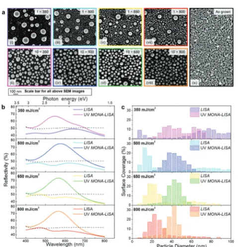
This LISA process with a UV laser (248 nm) is strongly fluence-dependent as demonstrated in the SEM images of Fig. 3a(i, iii, v, vii). The “as grown” sample is also shown in Fig. 3a(ix) for comparison. The Ag NP size distributions are generally bimodal, consisting of one set of coarse and one set of fine nanoparticles (NP). Increasing the laser fluence from 350 mJ cm−2to 800 mJ cm−2results in a decreasing difference between the two NP sets, as shown by the quantified SEM images (Fig. 3b, purple, cyan, yellow and red bars). The bimodal NP size distributions are accompanied by two corres-ponding LSPR peaks in the optical reflectivity spectra (Fig. 3c, purple, cyan, yellow and red lines). The coarse particles are
Fig. 2 (a) Calculated vertical absorption profile for the 40 nm diameter Ag nanoparticle in units of percent per nanometer. Indicated with the two dashed lines are the two primary wavelengths used in this study. (b) Absorption percentage per nm profile in our model structure for the two principal wavelengths used in the study. (c) Measured temporal profile of the two laser sources used. (d) Corresponding temperature transients developed in the Ag NP, normalized to the laserfluence. (e) Calculated global map showing the peak temperature developed in a Ag NP on top of Si as a function of laser wavelength and NP size. The dashed lines indicate the two primary wavelengths used in this study.
Fig. 3 (a) SEM images of samples processed with LISA (1 pulse, 248 nm
LA) and UV MONA-LISA (10 pulses, 248 nm) under various applied
fluences (i–viii), including the as grown sample (ix). (b) The effect of LISA and UV MONA-LISA on the optical reflectivity spectra of a 10 nm Ag thin
film under various applied fluences. The spectra of the as grown is shown with a dashed line for comparison. (c) Surface coverage of the nanoparticles in relation to the particle diameter for all the cases of (a).
Nanoscale Paper
Open Access Article. Published on 21 March 2016. Downloaded on 23/06/2016 09:41:34.
This article is licensed under a
Creative Commons Attribution 3.0 Unported Licence.
[image:5.595.50.286.48.369.2] [image:5.595.308.548.390.639.2]accompanied by a region of depleted Ag around them, indicat-ing that they are formed in the expense of the fine particlesvia
surface diffusion and an Ostwald ripening process. At higher fluence the Ostwald ripening process becomes less pro-nounced and results into a higher population of fine particles and a smaller size of the coarse particles. This behaviour indi-cates that the process is more thermal for lower fluence, which superficially contradicts the simplified thermal description. In fact, the higher fluence is sufficient to produce hot electrons during the pulse,25resulting into ionization and positive char-ging of Ag nanoparticles. This hinders the Ostwald ripening process viaCoulomb repulsion among the nanoparticles and stabilizes them in well separated distances. This argument is further supported by considering the results of the LISA process with a 193 nm laser (see the ESI, section 1.2, page 5, Fig. S4†). Indeed, for the 193 nm UV LA the bimodal distri-bution is less pronounced, even for the lower fluence, due to the higher ionization probability of Ag when irradiated by higher energy photons. On the contrary, LISA is not possible at all for long wavelengths, e.g. the 532 nm used in this work, due to the high reflectivity of metallic layers at these wavelengths.
The modification of nanoparticle assemblies by multiple laser pulses (MONA-LISA process) involves quite different physics due to the selective optical absorption and heat dissi-pation by the nanoparticles, as mentioned earlier. In order to demonstrate this, we subject the initial assemblies of nano-particles produced by LISA to a series of UV and/or VIS LA steps. We explore this process with the laser wavelengths 193, 248, 532 and 620 nm and combinations of them for a variety of fluences, number of sequential pulses and initial metal film thickness of 5 and 10 nm for Ag on a Si(100) substrate. Fur-thermore we investigate the process for Au and Cu thin films, deposited via sputtering (for more details refer to the ESI,† sections 1.3–1.4, page 6). Additionally, we demonstrate that our proposed process is independent to the thin film fabrica-tion technique by applying MONA-LISA to Ag film deposited
by e-beam evaporation as well as chemical reduction of AgNO3
(for more details refer to the ,†section 2.1.ii: page 34).
First we consider the case of UV MONA-LISA,i.e.processing by multiple UV (248 nm) laser pulses, and we correlate the effect of interband absorption with the size-selective heat dissi-pation; Fig. 3c shows the optical reflectivity spectra of a 10 nm Ag film recorded after UV MONA-LISA using 10 successive UV laser pulses at various fluences (magenta, blue, green and orange lines for 350, 500, 650, 800 mJ cm−2, respectively). Comparing these spectra with those for the previous LISA pro-cessing ( purple, cyan, yellow and red lines) reveals that the consecutive pulses transform the two reflectivity peaks to one, indicating a gradual transformation of the bimodal distri-butions to unimodal (reflectance data for intermediate cases of less than ten successive pulses are presented in the ESI, section 1.2: Fig. S4,†page 5). This is also confirmed by the corresponding SEM images in Fig. 3a(ii, iv, vi, viii) and the size distribution histograms in Fig. 3b (magenta, blue, green and orange bars), respectively. The reshaping of the particles is a combination of the disappearance of the coarse particles (by melting upon LA) and the enlargement of the surrounding fine particles, as they become the recipients of mass transfer from the melted coarse ones.
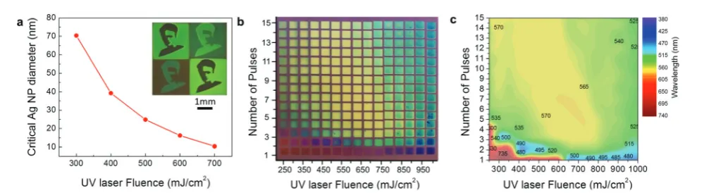
The physics behind that observation is based on the faster heat dissipation from the finer nanoparticles due to their higher effective surface (surface to volume ratio). As a result, the finer nanoparticles remain cold during UV MONA-LISA. This was quantified by photothermal calculations, which determine the equi-temperature contour linesvs.nanoparticle diameter, from which the critical size under which every par-ticle remains practically cold during the UV MONA-LISA process of Ag on Si can be inferred; assuming for simplicity the bulk Ag melting temperature of 960 °C, the calculated values of the critical diametervs. the fluence of the 248 nm laser are presented in Fig. 4a. Note that the critical diameter is strongly dependent on the thermal conductivity of the sub-strate, as a less thermally conductive substrate would hinder
Fig. 4 (a) Critical nanoparticle diameter (the diameter value under which every particle remains practically cold during the UV LA process; hence
these particles cannot be further manipulated upon irradiation) as a function of applied laserfluence. The inset shows an optical microscopy image of the“Marie Curie Actions”logo produced by projection mask under LISA/UV MONA-LISA. Each colour represents a different UV LAfluence. (b) A digital photo of a grid of LISA/UV MONA-LISA spots (2.5 × 2.5 mm2each) of varyingfluence (x-axis) and number of pulses (y-axis) produced on a
10 nm Ag thinfilm. (c) Contour plot of the dominant LSPR maximum acquired from optical reflectivity spectra from each spot of (b) (in the case of bimodal responses, the spectral value of the stronger reflectivity peak is reported).
Open Access Article. Published on 21 March 2016. Downloaded on 23/06/2016 09:41:34.
This article is licensed under a
[image:6.595.51.551.516.653.2]heat dissipation.34For example, SiC should behave very simi-larly to Si, having similar thermal conductivities (Si: 150 W m−1K−1, SiC: 140–180 W m−1K−1). The behaviour of MgO and Al2O3should also be similar as well, albeit would require lower
fluences to achieve similar nanoparticle arrangements due to their lower thermal conductivity (Al2O3: 25–30 W m−1 K−1,
MgO: 45–60 W m−1K−1). SiO2on the other hand is thermally
resistive enough (SiO2: 1.5–2 W m−1K−1) to probably change
the process,i.e.the heating and cooling rates would be much smaller, and so the particle shaping should be quite different.
The UV MONA-LISA process is thus based on the larger par-ticles having the ability to raise their temperature above their melting point, and consequently melting and re-solidifying forming smaller particles with a stochastic size distribution, while the smaller ones remain below the melting threshold and therefore remain practically unaffected. Evidently, succes-sive pulses suppress the population of the coarse particles, gradually transforming them to stable finer particlesvia sto-chastic size redistribution.
A secondary mechanism is observed as the laser fluence is increased to high values; in particular, above 700 mJ cm−2 a gradual decrease in the absolute reflectivity values is observed when several pulses are used (see ESI, section 1.1: Fig. S3,†page 4) indicating loss of material due to ablation, concomitantly with a slight blueshift of the LSPR peak (due to increased empty space between the nanoparticles). This mechanism is also observed for high fluence UV MONA-LISA processing at other wavelengths, such as the 193 nm (see ESI, section 1.1: Fig. S2, page 3 and section 1.2: Fig. S4,†page 5), and 355 nm (studied and reported by Stietz et al.35). In fact, ablation is observed at a lower fluence (650 mJ cm−2) for the 193 nm laser, due to the higher energy of the corresponding photons.
The wide range of size distributions achieved by LISA and UV MONA-LISA results in a vast colour palette as those pre-sented in Fig. 4b and c (real colour appearance of the Ag nano-particle assemblies and quantitative spectral reflectivity response, respectively), which quantifies UV MONA-LISA as a process most capable for tuning the size and distribution of NPs and thus their plasmonic resonance wavelength, spanning from 480–735 nm as shown in Fig. 4c. Combining the LISA and MONA-LISA process with projection masks may produce multi-colour images of high spatial resolution and multi-colour contrast as that presented in the inset of Fig. 4a, depicting the logo of the
“Marie Curie Actions”(People Programme–EU:FP7).
[image:7.595.307.547.286.574.2]The implementation of MONA-LISA employing exclusively UV pulses has the inherent limitation of not being able to probe nanoparticles of size below the critical size described in Fig. 4a. This has the severe consequence that only the coarse particles are affected after successive laser pulses. In order to directly probe and manipulate the finer particles we must exploit their selective optical absorption via LSPR using a visible laser wavelength that would result in stronger optical absorption and hence higher temperature rise, as predicted by the computational results presented in Fig. 2e.
The optimum condition for narrowing the bandwidth of the LSPR at 532 nm was achieved by applying 500 pulses at
125 mJ cm−2(refer to ESI, section 2.1: Fig. S7,†page 7). The fact that hundreds of VIS pulses are needed in order to induce a change reflects the lower temperature rise profile per pulse (compared to the UV processing where 10 pulses are enough to reach a steady state), as predicted by the computational results of Fig. 2e, where a lower temperature rise is evident at VIS wavelengths compared to UV processing.
Nevertheless, this combined process produces plasmonic nanoparticle assemblies with size distributions comparable to colloidal nanoparticles,17,36but crucially with our MONA-LISA method they are firmly attached on the substrate.
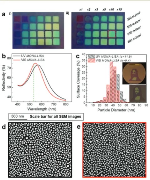
A broader view of the VIS MONA-LISA process, that demon-strates its selective nature, is obtained by considering its effect to Ag nanoparticle assemblies of varying size distributions. For this purpose we compare two grids of samples pre-processed by LISA and subsequently processed by VIS MONA-LISA and UV MONA-LISA (Fig. 5a, left-hand side and right-hand side, respectively). Each grid consists of square spots (2.5 ×
Fig. 5 (a) A digital photo of a grid of LA spots of varyingfluence (y-axis) and number of pulses (x-axis) produced on a 10 nm Ag thinfilm: (i) pro-ducedviathe LISA/UV MONA-LISA process and (ii) replica of (i) with sub-sequent VIS MONA-LISA treatment (combined UV and VIS laser annealing). (b) Optical response of a Ag/Si sample (initial effective thick-ness of 10 nm) after UV MONA-LISA (10 pulses, 248 nm at 650 mJ cm−2
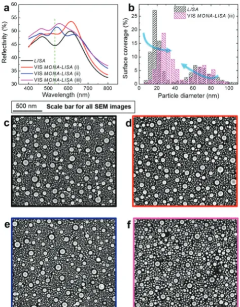
–black line) and UV+VIS MONA-LISA (10 pulses, 248 nm at 650 mJ cm−2and 500 pulses, 532 nm at 125 mJ cm−2–red line). (c) Surface coverage of the nanoparticles in relation to the particle diameter for the two spots indicated with red and black dashed boxes in (a) and with optical response shown in (b). Inset depicts two portraits of Da Vinci’s Mona Lisa validating the potential and scalability of the MONA-LISA process. (d) SEM image of the UV MONA-LISA sample. (e) SEM image of the UV+VIS MONA-LISA sample.
Nanoscale Paper
Open Access Article. Published on 21 March 2016. Downloaded on 23/06/2016 09:41:34.
This article is licensed under a
Creative Commons Attribution 3.0 Unported Licence.
2.5 mm2) pre-processed by 1, 2, 3, 5, 10 and 15 pulses of 248 nm at fluences of 350, 500, 650, 800 mJ cm−2. All spots on the left-hand side grid only were subsequently processed by VIS MONA-LISA with 500 pulses from a 532 nm laser (2nd har-monic from an Nd:YAG laser) at 125 mJ cm−2(round laser spot of 2 mm in diameter). After applying VIS MONA-LISA there is a remarkable change in their optical response. This is vividly illustrated in the left-hand side grid of Fig. 5a where the circu-lar Nd:YAG spot (the result of VIS MONA-LISA) is clearly distin-guished inside the excimer pre-treated square (the result of the UV LISA). The appearance of all VIS MONA-LISA spots shifts to green proving the reshaping of the nanoparticles to sizes that exhibit LSPR at the processing wavelength. In particular, if we consider the two spots indicated in Fig. 5a with a black and a red dashed box, the shift to green after VIS MONA-LISA is depicted in their optical reflectance spectroscopy data shown in Fig. 5b. Fig. 5c shows their particle size distributions, as cal-culated from image analysis of their corresponding SEM images (Fig. 5d and e), where it is clearly evident that the VIS MONA-LISA process creates a narrower size distribution around 40 nm diameter. This is also evident by the decrease of the standard deviation (σ) values (expressed in nm), which the VIS MONA-LISA process demonstrates. The values of σ are shown in Fig. 5c and present a measure of the variability of the size distribution of the nanoparticle array for each sample. Nanoparticles with LSPR close to the processing wavelength (532 nm) are less affected by the laser process due to their high reflectivity in that particular wavelength. The melting process requires a high temperature, which scales with the total absorption of the system. At the LSPR frequency the reflectivity becomes maximum and thus the total system absorption becomes minimum. However the rest of the par-ticles melt and upon re-solidification some of those will even-tually cool down to a size that is giving a resonance close to 532 nm. These nanoparticles will remain now practically cold and as this process evolves, the majority of the particles that prevail will be of that particular size.
This effect of VIS MONA-LISA is more pronounced in the cases of nanoparticle assemblies with optical response away from green: for example all the LISA pre-treated spots (first column in grid of Fig. 5a). Examining the later in more detail one can see that the LSPR created by the initial UV MONA-LISA process (248 nm, 2 × 350 mJ cm−2) exhibits a double reflec-tance peak, due to its bimodal nanostructuring, notably with no particular response close to 532 nm, as shown in Fig. 6a (black line, UV MONA-LISA). Applying VIS MONA-LISA to this area, with 500 pulses (i), 2000 pulses (ii) and 4000 pulses (iii) results in gradually changing the bimodal distribution to one with a peak very close to the processing wavelength (532 nm). Their nanoparticle distributions are presented in the histo-grams of Fig. 6b, as resulted from the corresponding SEM images shown in Fig. 6c–f. It is noteworthy that the VIS MONA-LISA probes particularly the finer Ag nanoparticles (<20 nm), confirming the computational analysis presented in Fig. 2e. Similar behaviour was observed using other visible wave-lengths. For example, applying VIS MONA-LISA at 620 nm onto
the above mentioned UV MONA-LISA sample produced by 248 nm with 2 × 350 mJ cm−2, results in a shift of the LSPR peak from∼650 nm to∼625 nm (refer to the ESI, section 2.3, Fig. S38,†page 35). This proves the general character of the VIS MONA-LISA approach and the flexibility of producing any selected plasmonic particle distribution by probing their LSPR absorption during visible laser annealing.
From the practical point of view, combining the two laser wavelengths (UV and VIS) and appropriately selecting the pro-cessing conditions (number of pulses and fluence), provides an unprecedented asset for tuning the nanoparticle assemblies into size distributions that are:
(i) Bimodal (UV LISA),
(ii) Multimodal (UV LISA and VIS MONA-LISA of intermedi-ate number of pulses),
(iii) Unimodal of a limited variation in size due to self-assembly and heat dissipation selectivity (UV MONA-LISA),
(iv) Unimodal of any size due to LSPR selectivity (UV MONA-LISA and VIS MONA-MONA-LISA at steady state).
Fig. 6 (a) Optical reflectivity spectra of UV MONA-LISA (2 pulses,
248 nm at 350 mJ cm−2–black line), used as a template for the sub-sequent VIS MONA-LISA (532 nm at 125 mJ cm−2) with 500 pulses (red line), 2000 pulses (blue line) and 4000 pulses (magenta line). The green dashed line sets the 532 nm mark. (b) Surface coverage of the nano-particles in relation to the particle diameter for all the cases of (a). (c) SEM image of the UV MONA-LISA processed sample. (d) SEM image of the VIS MONA-LISA (i) sample (500 pulses). (e) SEM image of the VIS MONA-LISA (ii) sample (2000 pulses) and (f ) SEM image of the VIS MONA-LISA (iii) sample (4000 pulses).
Open Access Article. Published on 21 March 2016. Downloaded on 23/06/2016 09:41:34.
This article is licensed under a
[image:8.595.308.545.49.352.2]The last case (iv) goes beyond any laser-driven process for particle formation reported so far, and provides enhanced control and selectivity on the particle formation, allowing us to drive them towards narrower distributions. At the same time, besides unimodal distributions the MONA-LISA process can also be tuned to produce multimodal distributions with broad-band optical response covering the entire visible range, which is of particular importance for example in solar harvesting applications.
The potential and scalability of the MONA-LISA process is finally demonstrated by the two portraits of Da Vinci’s“Mona Lisa”presented as insets in Fig. 5c. The upper inset is a macro-scopic, large-scale pattern created with two contact masks on a 2″Si wafer coated with 10 nm Ag ( purple areas correspond to a process of one pulse at 500 mJ cm−2, whereas the green areas to three pulses of the same fluence). It was realized by raster-ing the UV laser annealraster-ing with a pixel size of 2.5 × 2.5 mm2. On the contrary, the lower inset is a microscopic pattern (2.5 × 2.5 mm2) created on the same wafer in a single pixel proces-sing uproces-sing two projection masks. The resolution of the method may be further reduced to a feature size less than a micron (restricted only by the diffraction limit and taking into account that in this case we would need a 3D model to simu-late the process) by using appropriate photolithographic or projection masks.10
The UV MONA-LISA process has been also tested in Au and Cu thin films (shown in the ESI, section 1.3, 1.4, Fig. S5, S6† respectively, page 6). The results show that NP formation is possible albeit the successful processing window becomes nar-rower. Especially for Cu’s case, its LSPR is too deep into the red-IR range and the LSPR strength is more faint than that of Ag and Au, therefore the VIS MONA-LISA is not expected to be as effective.
Conclusions
Different optical absorption and heat diffusion mechanisms in plasmonic metal nanoparticles were taken into advantage as a means of controlling matter at the nanoscale,vialaser driven processes for restructuring a metal thin film into a pre-determined nanoparticle template.
The stochastic recrystallization of melted metal nano-particles by UV processing only is governed by the morphology of the particle template itself,i.e.the existence of a critical size diameter as a function of the laser fluence. This self-limiting process (that in some cases may well provide the desired outcome) could be overcome by the subsequent application of VIS processing, allowing a further modification to the nano-particles templates. This is due to the selective heat dissipa-tion from the nanoparticle size groups away from the VIS processing laser wavelength, providing an exceptional capa-bility for selective formation of nanoparticles with predesigned and desired size distributions. As a result, successive pulses of UV LA reduce the volume fraction of larger nanoparticles (>50 nm), while VIS LA may either further refine the size
distri-butions or induce the emergence of nanoparticles, which exhibit LSPR close to the irradiation wavelength. This com-bined UV and VIS LA treatment provides unprecedented control on the size distributions and plasmonic behaviour of nanoparticle arrays of noble metals (Ag, Au, Cu), indepen-dently of their deposition method and can create nano-particles with sizes and distributions that are otherwise impossible to produce by single wavelength UV laser anneal-ing. We have named this approach MONA-LISA: Modification of Nanoparticle Arrays by Laser-Induced Self Assembly.
Acknowledgements
N. Kalfagiannis acknowledges funding from People Pro-gramme (Marie Curie Actions) LASER-PLASMON of the Euro-pean Union’s Seventh Framework Programme (FP7/2007–2013) under REA grant agreement no. PIEF-GA-2012-330444.
A. Siozios and D. V. Bellas acknowledge funding from the following sources: the European Union (European Social Fund
– ESF) and Greek national funds through the Operational Program “Education and Lifelong Learning” of the National Strategic Reference Framework (NSRF) – Research Funding Program: Heracleitus II.
The research activities of P. Patsalas and E. Lidorikis that led to these results were co-financed by Hellenic Funds and by the European Regional Development Fund (ERDF) under the Hel-lenic National Strategic Reference Framework (NSRF) 2007–2013, according to contract no. 11ΣϒN-5-1280 of the Project ‘Nano-Hybrid’, within the Program ‘Competitiveness and Entrepreneurship’.
D. C. Koutsogeorgis acknowledges the School of Science and Technology at Nottingham Trent University for the approval of a sabbatical made possibleviaQR funds, and the Higher Edu-cation Funding Council for England (HEFCE) for providing the QR funds as a result of the Research Assessment Exercise 2008 (RAE2008).
The authors would like to acknowledge Dr B. Boudjelida, for providing access to a Dimension FastScan Atomic Force Micro-scope at BRUKER’s headquarter’s, Coventry, UK and Dr Robert Ranson for providing training on the Nd:YAG laser used for this work.
Notes and references
1 Z. H. Nie and E. Kumacheva,Nat. Mater., 2008,7, 277. 2 E. J. Menke, M. A. Thompson, C. Xiang, L. C. Yang and
R. M. Penner,Nat. Mater., 2006,5, 914.
3 J. Yang, T. Ling, W. T. Wu, H. Liu, M. R. Gao, C. Ling, L. Li and X. W. Du,Nat. Commun., 2013,4, 1695.
4 T. Scheibel, R. Parthasarathy, G. Sawicki, X. M. Lin, H. Jaeger and S. L. Lindquist,Proc. Natl. Acad. Sci. U. S. A., 2003,100, 4527.
5 J. Y. Cheng, A. M. Mayes and C. A. Ross,Nat. Mater., 2004,
3, 823.
Nanoscale Paper
Open Access Article. Published on 21 March 2016. Downloaded on 23/06/2016 09:41:34.
This article is licensed under a
Creative Commons Attribution 3.0 Unported Licence.
6 W. Lu and C. M. Lieber,Nat. Mater., 2007,6, 841.
7 M. W. Li, R. B. Bhiladvala, T. J. Morrow, J. A. Sioss, K. K. Lew, J. M. Redwing, C. D. Keating and T. S. Mayer,
Nat. Nanotechnol., 2008,3, 88.
8 J. Rongchao, C. YunWei, C. A. Mirkin, K. L. Kelly, G. C. Schatz and J. G. Zheng,Science, 2001,294, 1901. 9 M. J. Beliatis, N. A. Martin, E. J. Leming, S. R. P. Silva and
S. J. Henley,Langmuir, 2010,27, 1241.
10 A. Siozios, D. C. Koutsogeorgis, E. Lidorikis, G. P. Dimitrakopulos, T. Kehagias, H. Zoubos, P. Komninou, W. M. Cranton, C. Kosmidis and P. Patsalas,
Nano Lett., 2012,12, 259.
11 A. Stalmashonak, H. Graener and G. Seifert, Appl. Phys. Lett., 2009,94, 193111.
12 S. J. Henley, M. J. Beliatis, V. Stolojan and S. R. P. Silva,
Nanoscale, 2013,5, 1054.
13 D. G. Grier,Nature, 2003,424, 810.
14 J. R. Moffitt, Y. R. Chemla, D. Izhaky and C. Bustamante,
Proc. Natl. Acad. Sci. U. S. A., 2006,103, 9006.
15 T. L. Gustavson, A. P. Chikkatur, A. E. Leanhardt, A. Gorlitz, S. Gupta, D. E. Pritchard and W. Ketterle,Phys. Rev. Lett., 2002,88, 020401.
16 M. Potara, M. Baia, C. Farcau and S. Astilean, Nanotechno-logy, 2012,23, 055501.
17 M. J. Mulvihill, X. Y. Ling, J. Henzie and P. D. Yang,J. Am. Chem. Soc., 2010,132, 268.
18 N. T. Panagiotopoulos, N. Kalfagiannis, K. C. Vasilopoulos, N. Pliatsikas, S. Kassavetis, G. Vourlias, M. A. Karakassides and P. Patsalas,Nanotechnology, 2015,
26, 205603.
19 V. Giannini, Al. Fernandez-Dominguez, Y. Sonnefraud, T. Roschuk, R. Fernandez-Garcia and S. A. Maier, Small, 2010,6, 2498.
20 V. Giannini, Al. Fernández-Domínguez, S. C. Heck and S. A. Maier,Chem. Rev., 2011,111, 3888.
21 H. Zoubos, L. E. Koutsokeras, D. F. Anagnostopoulos, E. Lidorikis, S. A. Kalogirou, A. R. Wildes, P. C. Kelires
and P. Patsalas, Sol. Energy Mater. Sol. Cells, 2013, 117, 350.
22 N. Kalfagiannis, P. G. Karagiannidis, C. Pitsalidis, N. T. Panagiotopoulos, C. Gravalidis, S. Kassavetis, P. Patsalas and S. Logothetidis,Sol. Energy Mater. Sol. Cells, 2012,104, 165.
23 H. A. Atwater and A. Polman,Nat. Mater., 2010,9, 205. 24 F. Pincella, K. Isozaki and K. Miki,Light: Sci. Appl., 2014,3,
e133.
25 W. Nichols, G. Malyavanatham, D. Henneke, D. O’Brien, M. Becker and J. Keto,J. Nanopart. Res., 2002,4, 423. 26 E. Lidorikis, S. Egusa and J. D. Joannopoulos,J. Appl. Phys.,
2007,101, 054304.
27 A. Taflove and S. C. Hagness, Computational Electro-dynamics: The Finite-Difference Time-Domain Method, Artech House, Incorporated, 2005.
28 J. D. Jackson, Classical electrodynamics, Wiley, New York, NY, 3rd edn, 1999.
29 F. Schedin, E. Lidorikis, A. Lombardo, V. G. Kravets, A. K. Geim, A. N. Grigorenko, K. S. Novoselov and A. C. Ferrari,ACS Nano, 2010,4, 5617.
30 E. D. Palik, Handbook of Optical Constants of Solids, Aca-demic Press, 1998.
31 F. P. Incropera, Fundamentals of Heat and Mass Transfer, John Wiley & Sons, 2006.
32 D. R. Lide,CRC Handbook of Chemistry and Physics, Taylor & Francis, 85th edn, 2004.
33 S. Nolte, C. Momma, H. Jacobs, A. Tünnermann, B. N. Chichkov, B. Wellegehausen and H. Welling,J. Opt. Soc. Am. B, 1997,14, 2716.
34 A. Siozios, N. Kalfagiannis, D. V. Bellas, C. Bazioti, G. P. Dimitrakopulos, G. Vourlias, W. M. Cranton, E. Lidorikis, D. C. Koutsogeorgis and P. Patsalas, Nano-technology, 2015,26, 155301.
35 F. Stietz,Appl. Phys. A: Mater. Sci. Process., 2001,72, 381. 36 V. Mazumder, M. F. Chi, K. L. More and S. H. Sun,Chem.
Int. Ed., 2010,49, 9368.
Open Access Article. Published on 21 March 2016. Downloaded on 23/06/2016 09:41:34.
This article is licensed under a