Robustness Analysis and Experimental Validation of
a Fault Detection and Isolation Method for the
Modular Multilevel Converter
Shuai Shao, Alan J. Watson,
Member, IEEE,
Jon C. Clare,
Senior Member, IEEE
, Pat W. Wheeler,
Senior Member, IEEE
Abstract—This paper presents a fault detection and isolation (FDI) method for open-circuit faults of power semiconductor devices in a modular multilevel converter (MMC). The proposed FDI method is simple with only one sliding mode observer (SMO) equation and requires no additional transducers. The method is based on an SMO for the circulating current in an MMC. An open-circuit fault of power semiconductor device is detected when the observed circulating current diverges from the measured one. A fault is located by employing an assumption-verification process. To improve the robustness of the proposed FDI method, a new technique based on the observer injection term is introduced to estimate the value of the uncertainties and disturbances, this estimated value can be used to compensate the uncertainties and disturbances. As a result, the proposed FDI scheme can detect and locate an open-circuit fault in a power semiconductor device while ignoring parameter uncertainties, measurement error and other bounded disturbances. The FDI scheme has been implemented in a field programmable gate array (FPGA) using fixed point arithmetic and tested on a single phase MMC prototype. Experimental results under different load conditions show that an open-circuit faulty power semiconductor device in an MMC can be detected and located in less than 50ms.
Index Terms—Fault detection and isolation, modular multilevel converter, sliding mode observer.
I. INTRODUCTION
T
HE modular multilevel converter (MMC) is the state of the art in multilevel converters and is receiving great interest both from academia and industry. It has a number of desirable features such as modular configuration, low harmonic distortion, low voltage stress on the semiconductor devices, high voltage and high power capability and simple realization of redundancy [1]. In addition, the cells of an MMC are fed by capacitors and no multi-phase transformers are required. A comprehensive introduction of the operation of the MMC is given in [2]. The review paper [3] summarizes the latest achievements regarding the MMC in terms of modeling, control, modulation, applications and future trend.Power semiconductor switches are amongst the most failure prone components in a power converter and each of these devices is a potential failure point [4]. With large numbers of semiconductor devices, the possibility of fault occurrence
The authors are with the Power Electronics, Machines and Control Group, School of Electrical and Electronic Engineering, University of Nottingham, Nottingham NG7 2RD, U.K. (e-mail: [email protected]; [email protected]; [email protected]; Pat. [email protected]).
Manuscript received April 19, 2005; revised December 27, 2012.
is much larger than for normal two-level voltage source converters (VSCs). Faults in power semiconductor devices cause a power converter operating far away from its setting point and this abnormal operation cannot be overcome by a feedback controller. If the faulty operation is allowed, other devices may be damaged and a shut-down of the plant may follow. Therefore, it is vital to detect and isolate these faults immediately after their occurrence.
Fault detection and isolation (FDI) deals with detecting anomalous situations (fault detection) and addressing their causes (fault isolation) [5]. An FDI scheme can be imple-mented either by hardware method or analytical (software) method [5], [6]. Hardware FDI employs repeated components or additional sensors, and a fault can be obtained if the behaviour of the process components are different from the redundant ones, or the additional sensors detect anomalous signals. It is straightforward and reliable but increases the cost, size and hardware complexity of the plant. The basic idea of analytical FDI is to check the consistency between the actual system behaviour and its estimated behaviour [7]. The estimated behaviour can be obtained either from a math-ematical model of the system (for example using observers) or an analysis of the historical data (for example using data mining or neural networks). Although the algorithm is more sophisticated, the cost and hardware complexity of employing analytical method is less than that for hardware method. The application of the analytical FDI methods is boosted by the great advances of the computer technology in recent decades [6].
There are two types of faults seen in a fully controlled power semiconductor device: short-circuit fault (remains ON regard-less of the gate signal) and open-circuit fault (remains OFF regardless of the gate signal). Any short circuit fault needs to be detected within10µsto save the semiconductor devices from destruction and to avoid a shoot-through fault with the complementary device [8]. A short circuit in an insulated-gate bipolar transistor (IGBT) is usually detected using a hardware circuit, often with additional sensors and associate circuits. These sensors and circuits are usually integrated in a gate driver to form an active/smart gate driver [9], [10]. The additional sensors and circuits add extra cost and size to the system. Furthermore, these active gate drivers can fail themselves due to their complexity and hence decrease the reliability of the power converter.
open--1 -0.5 0 0.5 1
x 104
-2000 -1000 0 1000 2000
-500 0 500 1000 1500
0 0.05 0.1 0.15 0.2
1500 2000 2500 3000
[image:2.612.52.297.59.368.2]time (s)
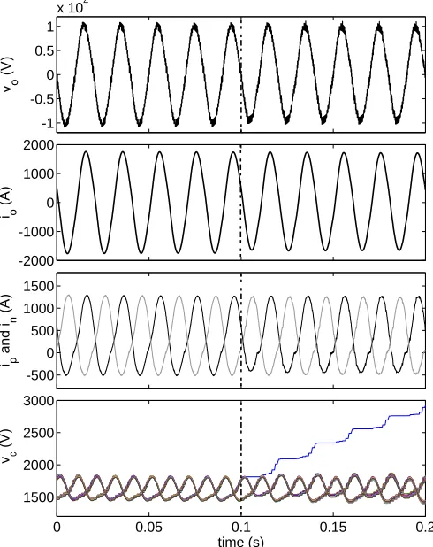
Fig. 1: Simulation results of an MMC with parameters same as an industrial 24MW MMC and an open-circuit fault occurs at 0.1s: from top to bottom, output voltage (vo), output current
(io), arm currents (ip andin) and capacitor voltages (vc).
circuit faulty switch in an MMC. The typical characteristics of an MMC in the event of an open-circuit fault in a power device is shown in Fig. 1 where the parameters are same as an industrial 24MW MMC [11] and an open-circuit fault occurred at 0.1s. Only one of the phases is considered. It can be seen that an open-circuit fault is not fatal immediately to an MMC, however the fault needs to be detected and removed within 0.1s to avoid secondary damages on other devices. The cause of an open-circuit fault can be various: lifting/fusing of bonding wires, a driver failure, or a communication problem between the controller and driver. The gate driver is recognised as the third most failure prone components according to an industry based survey [12]. The simplest detection method is to use an active gate driver as mentioned previously. Analytical redundancy can be used detect an open-circuit fault as this type of fault is not fatal immediately and can be tolerated by the power converter for some time [13]. Several analytical FDI methods based on the analysis of the output voltage waveform are reported. In [14], a faulty cell in a flying capacitor (FC) converter is detected and localized by analysing the switching frequency of the output phase voltage. This technique has also been applied to a cascaded H-bridge [15] where an open- or short-circuit fault can be detected. In [16], the characteristics of the output phase voltage are analysed in the time domain, and the occurrence of a fault is detected by the degradation of
the output voltage, while the fault is located by comparing the output phase voltage with all the possible phase fault voltages. In [17], an artificial intelligence (AI) FDI algorithm is proposed, where the historical data of the output phase voltages both in normal and faulty conditions are used to train a neural network. Survey [18] has presented a comprehensive review of the reliability of power electronics systems including methodologies of assessing reliability, methods to detect and locate faults as well as fault tolerate operation. Survey [19] has summarised the recent fault tolerance techniques for three phase voltage source converters.
A sliding mode observer (SMO) based FDI technique for an MMC was proposed in [20], [21], where a faulty power semiconductor device can be detected and located within 100ms. The work presented in this paper is an improved method. This method is simpler using only one SMO equation, and can detect and locate an open-circuit fault in less than 50ms. Furthermore, a technique is proposed to compensate for any parameter uncertainties, measurement errors and other bounded disturbances. The resultant FDI scheme can detect an open-circuit faulty power semiconductor device while rejecting any uncertainties and disturbances. The practical implementation of the SMO based FDI scheme in an FPGA (field programmable gate array) is also discussed in this paper and the experimental results at different load conditions are presented.
II. SLIDING MODE OBSERVER
A. Introduction
An observer is a mathematical replica of a system to esti-mate its internal states, driven by the input of the system and a signal representing the discrepancy between the estimated and actual states [22]. In the earliest observers such as the Luenberger observer, the differences between the estimated outputs and the actual outputs of the plant are fed back to the observer linearly, and the estimated states cannot converge to the measured states in the presence of a disturbance [22], [23]. The sliding mode observer employs a high-gain switching function of the discrepancy between the estimated and actual outputs to force the estimated states to the actual states asymptotically.
A first order system (1) is used in this paper:
˙
x=ax+u. (1)
An SMO for (1) is introduced:
˙ˆ
x=axˆ+bu+Lsgn(x−xˆ) (2)
sgn(x) =
1 x >0 0 x= 0
−1 x <0,
(3)
where ˆx donates the estimated/observed state of x and L
denotes the observer gains designed to drive xˆ → x in finite time. Subtracting (2) from (1) yields the dynamic error between the observed and measured states:
˙˜
Choosing L >|ax˜|, we obtain
˜
xx˙˜= ˜x(a˜x−Lsgn(˜x)) =|x˜|(|ax˜| −L)<0, (5) which will forcex˜andx˙˜to zero and keep zero thereafter, this motion along a line is the so-called sliding mode[24].
B. Sliding mode observer for an MMC
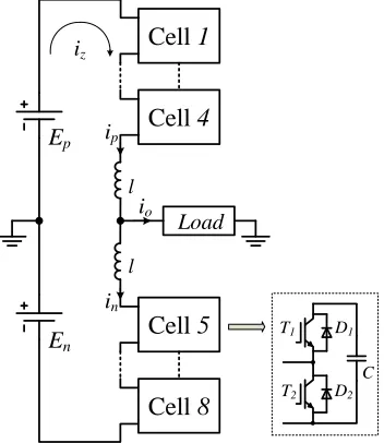
An SMO can be built for an MMC based on (2). In this paper a single-phase eight-cell MMC is considered, neverthe-less, the method is versatile and can be used for MMC with hundreds of cells.
The circuit diagram and parameters of the MMC used for the analysis and simulation are presented in Fig. 2 and Table I. T1 and T2 in Fig. 2 represent the upper and lower power
semiconductor devices in a cell.
l
l
E
pE
nLoad
Cell 4
Cell 5
Cell 8
Cell 1
ip
in
C T1 D1
T2 D2 io
[image:3.612.88.264.269.472.2]iz
[image:3.612.314.562.418.537.2]Fig. 2: The single-phase eight-cell MMC converter used for simulation.
TABLE I: Circuit parameters used in the simulation.
DC voltage Ep+En 6000V
Average circulating current Iz 120A
Nominal voltage of the cell capacitors Vc 1500V
Capacitance of cell capacitors C 4mF Inductance of the arm inductors l 3mH
Load 5Ω,4mH
According to the Kirchhoffs voltage law (KVL), we obtain the following equation for the MMC (Fig. 2):
ldip dt +l
din dt =−
8 X
i=1
Sivci+Ep+En (6)
whereipandin are the upper and lower arm currents,lis the
inductance of arm inductors,Ep andEn are the DC voltages, vciandSi are the capacitor voltage and switching state of the
Celli respectively.Si is defined in Table II, whereg1 andg2
are the gate signals for the upper and lower switch in a cell.
TABLE II: Switching stateS in normal conditions
S Driving signals
1 g1= 1, g2= 0
0 g1= 0, g2= 1
Since the circulating current of the MMC converter isiz=
(ip+in)/2 [25], (6) can be rewritten as
2ldiz dt =−
8 X
i=1
Sivci+Ep+En. (7)
Based on (2) and (7) an SMO can be obtained for the MMC:
dˆiz dt =−
1 2l
8 X
i=1
Sivci−Ep−En !
+Lsatiz−ˆiz
(8)
It is noted that a saturation function sat(x) (9) is utilized instead of sgn(x) for less chattering of the observed states according to [26].
sat(x) =
1 x≥h
x/h −h<x < h, h >0
−1 x≤ −h
(9)
wherehis a constant.
A simulation has been carried out in SIMULINK/PLECS to verify the SMO (8). The parameters of the MMC are listed in Table I and the observer gain L is 6×10⁴ and h = 1. Fig. 3 shows the simulation results where it can be seen that
ˆiz follows iz closely.
0 0.02 0.04 0.06 0.08 0.1
50 100 150 200 250
i z
(A
)
Time (s)
Actual current Observed current
Fig. 3: Simulation waveforms ofiz andˆizwhen the MMC is
fault free.
III. FAULT DETECTION AND ISOLATION USINGSMO
A. Mathematical Basis
Thefault detectionis firstly considered and a fault is added to the first order system
˙
x=ax+bu+kf (10)
wheref represents the value of the fault andkthe correspond-ing coefficients. It is noted thatf is often a very large value and cannot be overcome by the feedback control.
The difference between the observed and measured states can be obtained by subtracting (10) from (2):
˙˜
If we choose
L <|kf|, (12)
then at the faulty condition x˜1x˙˜1 > 0, the observer cannot
enter the sliding mode and xˆ will diverge from x signif-icantly. For an open circuit fault at Cell i in the MMC,
f = vci/(2l), ki = 1 and therefore L needs to satisfy the
following condition to detect an open-circuit faulty switch:
L < vci/2l. (13)
The occurrence of a fault can be detected by comparing |x−xˆ|with a given threshold value.
For the fault isolation an assumption-verification method was proposed [20], [21]. The procedure is to assume a location for the fault, modify the observer equation accordingly and to again compare the observed states with the measured states.
ˆ
xwill converge toxif the assumption is correct. In this case
kf is included in the observer as well:
˙ˆ
x=axˆ+bu+kf+Lsgn(x−xˆ) (14) Subtracting (14) from (10) yields the dynamical error:
˙˜
x=ax˜−Lsgn(˜x), (15) which is the same as (4) where sliding condition x˜x <˙˜ 0 is satisfied and xˆ→x in finite time. On the other hand, if the assumed fault location is incorrect,xˆwill keep diverging from
x. In this way the fault can be located.
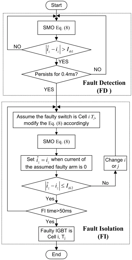
B. Flowchart
The flowchart of this algorithm is shown in Fig. 4. There are two modes in this algorithm: FD (fault detection) mode and FI (fault isolation) mode:
[FD mode] This mode monitors whether a fault occurs. If the difference between the observed and measured circulating current |iz−ˆiz|is larger than a threshold value Ith1 and this
condition persists for0.4ms, then an open-circuit fault occurs and the FDI scheme enters FI mode; otherwise the FDI scheme stays in FD mode.
[FI mode] This mode locates where is the open-circuit fault. The assumption-verification process is employed. TheCell i, Tjis assumed to be the faulty device, the switching stateSiin
SMO (8) is modified according to Table II in [20]. If Cell i, Tj is the actual faulty device, ˆiz converges to iz, otherwise
ˆiz diverges from iz. It is important to note that during some
points in the faulty period the current of the faulty arm can be clamped to zero because of the fault, and the converter is unobservable in these moments. Thereforeˆizis set toˆiz=iz
[image:4.612.331.544.58.475.2]when the current of the assumed faulty arm is 0 as shown in Fig. 4.
It is noted that the threshold values Ith1 andIth2 are load
dependent. In the case of faulty power semiconductor device,
ˆiz diverges from iz slower under light load than that under
heavy load. The divergence rate between ˆiz and iz is also
related to the observer gain L according to (11). There are
Persists for 0.4ms?
Assume the faulty switch is Cell i Tj,
modify the Eq. (8) accordingly
Faulty IGBT is Cell i, Tj
Change i
orj
Start
YES
YES
NO
No
Yes
Fault Detection (FD )
Fault Isolation (FI)
SMO Eq. (8)
FI time>50ms
Yes
End NO
1 ˆ
z z th
i i I
2 ˆ
z z th
i i I SMO Eq. (8)
ˆ
z z
i i
Set when current of the assumed faulty arm is 0
Fig. 4: Flowchart of the FDI method for an MMC.
many choices forIth1andIth2and, for example, one of them
can be:
L= Iz
Izo
Lo, L≥ Lo
8
Ith1= 2Iz, Ith1≥ Izo
2
Ith2=Iz, Ith2≥ Izo
4
(16)
whereLodenotes the observer gain under the full load,Izthe
circulating current,Izo the circulating current under full load.
As shown in (16), it is recommended thatL, Ith1andIth2are
larger than certain values to reject the parameter uncertainties and measurement noise.
Simulations have been carried out to verify the proposed algorithm with the parameters listed in Table I. L needs to satisfyL < Vc/2l= 2.5×10⁵according to (12), andLis set
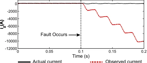
In Fig. 5 to 7, an open-circuit fault occurs at Cell 1, T1
at 0.1s. In Fig. 5, no FDI scheme is applied andˆiz diverges
from iz at a very high rate after the occurrence of the fault.
In Fig. 6 and 7, the FDI algorithm enters FI mode once |iz−
ˆiz|> Ith1 persists for 0.4ms. The FI mode is indicated with
a grey background. In Fig. 6 the assumed faulty switch is the actual one andˆiz converges to iz in FI mode; in Fig. 7 the
assumed faulty switch is Cell 2, T1, which is not the actual
faulty device,ˆiz diverges fromiz in FI mode and|ˆiz−iz|> Ith2in 50ms.
0 0.05 0.1 0.15 0.2
-12000 -10000 -8000 -6000 -4000 -2000 0
i z
(A
)
Time (s)
Actual current Observed current
[image:5.612.314.562.55.216.2]Fault Occurs
Fig. 5: Simulation waveforms of iz and ˆiz when an
open-circuit fault occurs at Cell1, T1 at 0.1s.
-400 -200 0 200
0 0.05 0.1 0.15 0.2 0.25
0 200 400 600
Time (s) iz
(A
)
(A
)
th2 Measured Observed
I
ˆ
z
z
i
i
−
Fig. 6: Simulation results of FDI: the open-circuit fault occurs atCell 1, T1 and the assumed faulty switch isCell 1, T1.
IV. ROBUSTNESSANALYSIS AND DISTURBANCE COMPENSATION
In any analytical FDI scheme certain assumptions including accurate physical parameters, precise measurements and linear, time-invariant operation are made when modelling a plant [5]. However, these assumptions may not be accurate. The pa-rameters may contain uncertainties, for example the parasitic resistance of an inductor, and may degrade over time. Mea-surements usually have errors superimposed on the signals. These errors can include electronic white noise and incorrect scaling factors between the measured and actual variable. Furthermore all dynamical plants are non-linear, but behave almost linearly. These uncertainties and disturbances may lead to divergence between the actual system behaviour and its
-400 -200 0 200
0 0.05 0.1 0.15 0.2 0.25
0 200 400 600
Time (s)
i z
(A
)
(A
)
th2 Measured Observed
I
ˆ
z
z
i
i
[image:5.612.52.301.189.297.2]−
Fig. 7: Simulation results of FDI: the open-circuit fault occurs atCell1, T1 and the assumed faulty switch is Cell2, T1.
estimated behaviour, giving false alarms. The robustness of an FDI scheme is the degree to which the system can maximise the sensitivity of the detection of actual malfunctions whilst discriminating between apparent faults and disturbances due to measurement noise, parameter uncertainty or transients [5].
The desirable features of this FDI method are:
• White noise in the measurement dose not affect the observed states, so it does not affect the FDI.
• The value of the parameter uncertainties, scaling errors in the measurements and other bounded disturbance is estimated using the observer injection term, this estimated value is used to compensate for the uncertainties and disturbances.
In summary, the proposed method is able to detect and locate an open circuit fault of a power semiconductor device whilst ignoring parameter uncertainties, measurement noise or other bounded disturbances. This desirable feature will be discussed in this section.
A. Mathematical basis
The first order system (1) and its SMO (2) are considered to demonstrate the features described above. By adding the uncertainties and disturbances to (2), we obtain
˙ˆ
x= (a+ ∆a)ˆx+ (b+ ∆b)(u+ ∆u) +d+Lsgn(x−xˆ)
(17)
where∆aand∆bdenote the values of parameter uncertainties,
∆u the value of the measurement noise consisting of white noise∆rand a scaling error between the measured and actual variable∆s. It is assumed that the values of these uncertainties and disturbances are bounded and are smaller than the value of a fault.
Subtracting (17) from (1) we obtain the errors between the measured and observed states:
˙˜
x=ax˜−
D
z }| {
(∆axˆ+ ∆b(u+ ∆u) +b1∆u+d1)−Lsgn(˜x)
[image:5.612.50.299.355.514.2]If we choose Lsatisfying:
L >|ax˜|+|D|, (19) then x˜x <˙˜ |x˜|(|ax˜|+|D| −L)<0, the sliding mode in (18) occurs and x˜ → 0 (namely xˆ → x) in finite time. xˆ is not affected by the uncertainties or the disturbances.
Based on (12) and (19), the observer gain needs to satisfy the following condition to discriminate an open-circuit fault from uncertainties and disturbances:
|ax˜|+|D|< L <|kf| (20) Two simulations have been carried out to verify the above analysis. In these simulations the parameter uncertainties and measurement noise are added to the observer, all other condi-tions are the same as for Fig. 6 and 7. An open-circuit fault in Cell 1, T1 occurred at 0.1s and in FI mode the assumed
faulty switch is the actual one. In the first simulation (Fig. 8)
5%white noise is added to all the measurements as shown in (21). In the second simulation (Fig. 9) parameter uncertainties and1%scaling errors in measurements are added to the SMO as shown in (22).
iz(mes)= (1 + 5%r1)iz vci(mes)= (1 + 5%r2)vci ep,n(me)s= (1 + 5%r2)ep,n
(21)
ˆ
l= (1 + 0.1)l Rl= 0.05Ω
iz(mes)= (1 + 0.01)iz vci(mes)= (1−0.01)vci ep,n(mes)= (1 + 0.01)ep,n.
(22)
where the subscript mes denotes measured variables, r1, r2
andr3 are random numbers ranging from -1 to 1 and change
at every calculation cycle, ˆl denotes the inductance used in the observer, Rl denotes the parasitic resistance of the arm
inductors.
In the fault free condition it can be seen in Fig. 8 and 9 thatˆiz converge to iz and is not affected by the uncertainties
and disturbances. It can also be seen in Fig. 8 that white noise in the measurements does not affect the fault isolation which is indicated with grey background. Since the average value of the white noise is zero its effect on the observer is self-cancelling and therefore the observer and FDI scheme are not affected. However, parameter uncertainties and scaling errors in the measurements will lead to incorrect fault isolation. As shown in Fig. 9, there is noticeable difference between theˆiz
andiz. Larger observer gain and threshold values can be used
to alleviate the incorrect fault isolation, but more time will be needed to detect and locate a fault.
B. Compensation of uncertainties and disturbances
In this section the value of parameter uncertainties, scaling errors in the measurements and other bounded disturbances are estimated and this estimated value is used to compensate the observer to achieve robust FDI.
0 0.05 0.1 0.15 0.2 0.25
-300 -200 -100 0 100 200
i z
(A
)
Time (s)
[image:6.612.313.560.57.175.2]Actual current Observed current
Fig. 8: Simulation results ofˆiz and iz with 5% white noise
on the measurement.
0 0.05 0.1 0.15 0.2 0.25
-300 -200 -100 0 100 200
i z
(A
)
Time (s)
Actual current Observed current
Fig. 9: Simulation results ofˆiz andiz with parameter
uncer-tainties and systematic measured error.
Once (18) enters the sliding mode,x˜→0 andx˙˜→0 and it can be obtained:
D=−Lsgn(˜x) (23)
When the MMC is fault free (0 to 0.1s in Fig. 8 and 9) the uncertainties and disturbances D is counterbalanced by the observer injection term −Lsgn(˜x) according to (23). Therefore the value of D can be extracted from−Lsgn(˜x). Since −Lsgn(˜x) is a high frequency switching term, a low pass filter is applied to obtain the estimated value ofD:
ˆ
D= −Lsgn(˜x)
1 +τ s (24)
whereDˆ denotes the estimated value of the uncertainties and disturbances, and τ denotes time constant of the low pass filter. A simulation has been undertaken with the white noise (21), scaling errors and parameter uncertainties (22), and the simulation results are shown in Fig. 10. The value of Dˆ is about 20000 A/s and is caused by the parameter uncertainties and scaling errors in the measurements (the effect of the white noise is self-cancelling). Because of the uncertainties and disturbances, the observer injection term Lsgn(˜iz) operates
[image:6.612.303.562.238.364.2]isolation is caused. In order to achieve robust FDI,Dˆ is added to SMO to compensate for the uncertainties and disturbances:
dˆiz dt =−
1 2l
8 X
i=1
Sivci−Ep−En !
+Lsatiz−ˆiz
−Dˆ
(25)
It is noted thatDˆ only updates when the system is fault free.
0 0.05 0.1 0.15 0.2 0.25 0.3 0.35 0.4
-0.5 0 0.5 1 1.5 2 2.5
3 x 10⁴
[image:7.612.313.562.56.214.2]Time (s) ˆD(A/s)
Fig. 10: Simulation results of Dˆ (estimated value of the uncertainties and disturbances).
Simulations have been carried out to test the FDI with compensation of the uncertainties and disturbances. The white noise (condition (21)), parameter uncertainties and scaling errors in measurements (condition (22)) are considered. Dˆ is added to compensate for the uncertainties and disturbances. Simulation results are shown in Fig. 11 and 12. It can be seen in Fig. 11 and 12 that the uncertainties and disturbances are compensated and the open-circuit fault can be detected and lo-cated without influenced by the uncertainties and disturbances.
-400 -200 0 200
0.3 0.35 0.4 0.45 0.5 0.55
0 200 400 600
Time (s)
i z
(A
)
(A
)
th2 Measured Observed
ˆ
z
z
i
i
[image:7.612.51.299.164.276.2]− I
Fig. 11: Simulation results of FDI with uncertainties and disturbances: open-circuit fault at Cell 1, T1 and assumed
faulty device atCell 1, T1.
V. EXPERIMENTAL VALIDATION OF THEFDIMETHOD
An MMC experimental rig has been built to validate the fault detection and isolation method. The method is mented in an FPGA using fixed-point arithmetic. The imple-mentation procedures and experimental results are presented in this section.
-400 -200 0 200
i z
(A
)
0.3 0.35 0.4 0.45 0.5 0.55
0 200 400 600
Time (s)
(A
)
th2 Measured Observed
ˆ
z
z
i
i
− I
Fig. 12: Simulation results of FDI with uncertainties and disturbances: open-circuit fault at Cell 1, T1 and assumed
faulty device atCell2, T1.
A. The Experimental Rig
Measurement Board
Control Platform V, I
PWM
l
Load
Cell
1
Cell
4
Cell
5
Cell
8
l
DC bus MMC
T1
R1
T2
R2
C1
C2
ep
[image:7.612.314.559.325.474.2]en
Fig. 13: Diagram of the experimental MMC rig.
Fig. 14: Photograph of the experimental rig.
[image:7.612.50.299.441.598.2] [image:7.612.313.564.520.673.2]Fig. 15: Photograph of the assembled power module with gate driver and heatsink.
[image:8.612.332.545.59.135.2]module is soldered to a module interface board and attached to a heatsink. The cell capacitances are selected such that the ripple of the capacitor voltages is less than10%[27] and arm inductances are chosen such that the switching harmonic is less than 60% of the nominal circulating current. The parameters of the experimental rig are listed in Table III.
TABLE III: Circuit parameters used in the experiments.
Rated power P 2.5kW
Average circulating current Iz 5.2A
Nominal voltage of the cell capacitors Vc 120V
Capacitance of cell capacitors C 1.5mF Inductance of the Arm inductors l 2.6mH
IGBT modules F4-50R06W1E3
Voltage transducer LEM LV 25-P Current transducer LEM LA 55-P
DSP TMS320C6713
FPGA Actel A3P1000
The control scheme of the MMC experimental rig is shown in Fig. 16. The subscriptspandndenote the upper and lower arms respectively. Kv(s)andKi(s)are the PI compensators
for the regulation of the average capacitor voltages, GP R(s)
is a proportional resonant (PR) compensator to suppress the second harmonic of the MMC circulating current. The details of these compensators are listed in Table IV.vz is the output
of the these compensators and Vo∗ is the command for the AC voltage. Modulation indices for the upper and lower arms
mp and mn can be obtained with vz and Vo∗. mBi is the
term for balancing the capacitor voltages and can be obtained using block diagram shown the Fig. 17. mi,p and mi,n are
[image:8.612.317.564.409.570.2]the modulation indices for Celliin the upper and lower arms respectively. The phase-shifted PWM is used to generate gate signals for the IGBTs.
TABLE IV: Details of the compensators.
Ki(s) kp1+ksi1 kp1= 6.3, ki1= 500 Kv(s) kp2+kis2 kp2= 0.66, ki2= 74 GP R(s) kp3+s2+22kiω3cωcss+ωo2
kp3= 0.1, ki3= 80
ωc= 5, ωo= 200π
+
1
ci
v
1: ,
0
1: ,
0
p n
p n
i i
i i
V
ci:
1~8
1
c
V
m
Bi-
0.35
Fig. 17: Block diagram of the capacitor voltage balancing [28].
B. FPGA implementation of the SMO
The sliding mode observer is implemented in the FPGA to obtain the quasi-analog behaviour of the observed states. The observer is implemented using fixed point as there is no floating point unit (FPU) in the A3P1000 FPGA. The implementation includes three steps.
Step 1: Convert the analog observer into discrete form. Using x˙i[k] = (xi[k+ 1]−xi[k])/Ts, the discrete sliding
mode observer (8) can be expressed as
ˆiz[k+ 1] =ˆiz[k]−Ts
2l 8 X
i=1
Sivˆci[k]−ep[k]−en[k] !
+TsLsat ˜iz[k] (26) Step 2: Scale the actual variables iz[k], vci[k], ep,n[k] in
(26) to the digital variables Iz[k], Vci[k], Ep,n[k] sensed by
the A/D converters. The relationships between values of actual variables and the values of the corresponding digital variables are
iz[k] =mIIz[k]
vci[k] =mVVci[k], i= 1,· · ·8 ep[k] =mEEp[k], en[k] =mEEn[k],
(27)
wheremI, mV andmE are the scaling factors.
Substituting (27) into (26) we obtain
ˆiz[k+ 1] = ˆiz[k]−
T erm1
z }| {
mVTs
2mIl 8 X
i=1
SiVci[k] !
+
T erm2
z }| {
mETs
2mIl
(Ep[k] +En[k]) +
T erm3
z }| {
LTs mI
sat mI˜iz[k]
(28)
Step 3:Convert the parameters from floating point to fixed point and implement the observer in the FPGA usingVerilog. The observer equations are break down into three parts as shown in (28). The block diagram of FPGA program is illus-trated in Fig. 18. The subtraction is performed by adding the complement of the subtracted number and the multiplication is carried out by shifting.
C. Experimental results
[image:8.612.72.278.681.735.2]e
pLoad
+
i
pi
nv
oN
Cells
N
Cells
-r
al
al
ar
a1 2N
*
* 1
2 2
1
2 2
o z
p
o z
n
V v m
E V v m
E
12 ,
ci p
v
,
ci n
v
v
cp
i
n
i
*
o
V
z
v
p
m
n
m
,
i p
S
,
i n
S
*
c
V ( )
V
K s +- K si( )
+
-( ) PR
G s
-0 +
+ +
Controller
z
i
,
Bi p
m
, Bi n
m
PS-PWM
+
Balance ,
i n
m +
++
,
i p
m
[image:9.612.136.472.61.256.2]e
nFig. 16: The control scheme of the MMC experimental rig.
Sampling
Vc1[k]~ Vc8[k] Vc1~Vc8
Ip, In
Ep, En clock(100kHz)
S1~S8
Ep[k], En[k]
S1[k]~S8[k]
Ip[k], In[k]
+
+
+
Sampling Term1
Term2
Term3
ˆ [ 1]z
I k
+ ˆ [ ]z
[image:9.612.314.564.301.417.2]I k
Fig. 18: Block diagram of the experimental implementation of the SMO.
0 0.1 0.2 0.3 0.4 0.5 0.6 0.7 0.8
-2800 -2600 -2400 -2200 -2000
Time (s)
ˆ
(A/s)D
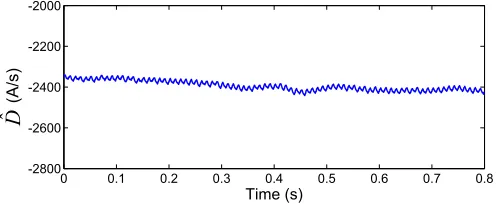
Fig. 19: Experimental results of Dˆ (estimated uncertainties and disturbances).
experimental results shown in Fig. 19 to 22, the MMC rig operates under full load condition with a circulating current
Izo = 5.2A. The observer gain L needs to satisfy condition
(13):L < Vc/(2l) = 2.5×10⁴ and1.2×104 is chosen forL
andh= 0.25.
In these experimental tests, parameter uncertainties and measurement noise are considered: 10% error in the induc-tance l, 0.11Ω parasitic resistance in the arm inductors and
5% scaling error in the measurement of the ep. A low pass
filter with a time constant of 0.1s is used to filter the switching
0 0.05 0.1 0.15 0.2
-100 -50 0 50
i z
(A
)
Time (s)
Measured current Observed current
Fault Occurs
Fig. 20: Experimental results ofizandˆizwhen an open-circuit
fault occurs at an IGBT at 0.1s.
frequency of−Lsgn(˜x)as shown in (24). This filter is imple-mented in the DSP. The estimated value of the uncertainties and disturbances is about -2400 A/s, as shown Fig. 19. This estimated value is put into the observer to compensate for the uncertainties and disturbances. In the experimental results in Fig. 20 to 26 this compensation has been added.
Fig. 20 shows experimental waveforms of the fault occur-rence. An open-circuit fault occurs at Cell 6, T1 occurs at
0.1s, no FDI algorithm is applied here. Before the fault,ˆiz
followsiz closely; after the fault occurrenceˆiz diverges from iz significantly.
Fig. 21 and Fig. 22 show waveforms with different assumed fault locations. In these two figures, an open-circuit fault occursCell 6, T2 at 0.1s. At full load the circulating current
is 5.2A and the threshold values for FDI are chosen as
Ith1 = 10.4A, Ith2 = 5.2A according to (16). Ith2 = 5.2A
is indicated using a black dash line. In Fig. 21, the assumed faulty switch is the actual one–Cell 6, T2,ˆiz converge toiz;
in Fig. 22, the assumed faulty switch isCell7, T2,ˆizdiverges
fromiz.
[image:9.612.52.297.303.400.2] [image:9.612.52.300.460.562.2]-10 0 10 20
i z
(A
)
0 0.05 0.1 0.15 0.2 0.25
0 5 10 15 20
(A
)
Time (s) Measured
Observed
ˆ
z
z
i
i
[image:10.612.315.562.55.219.2]− Ith2=5.2A Ith2=2A
Fig. 21: Experimental results of the FDI: an open-circuit fault occurs at Cell 6, T2 and the assumed faulty device is Cell 6, T2.
-10 0 10 20
0 0.05 0.1 0.15 0.2 0.25
0 5 10 15 20
Time (s)
iz
(A
)
(A
)
ˆ
z
z
i
i
−
Measured Observed
5
2 5.2A
th
[image:10.612.51.297.56.218.2]I = Ith2=2A
Fig. 22: Experimental results of the FDI: an open-circuit fault occurs at Cell 6, T2, while the assumed faulty device
is Cell7, T2.
to (16) the observer gain and threshold value have been chosen as L= 1500, Ith1= 5.2A, Ith2= 2.6A(the black dash line).
An open-circuit fault occurs at Cell 5, T1 at 0.1s. It can be
seen that the open-circuit fault can be located in 50ms. Transient operation does not disturb the proposed FDI method. An experimental test is undertaken with modulation index of the AC voltage changes from 0.6 to 0.95 at 0.07s and changes back at 0.12s. The experimental results are shown in Fig. 25 where ˆiz follows iz nicely regardless of the iz
fluctuation.
D. Discussion on the detection time
The choice of threshold value in a fault detection system such as the one we have described is always a compromise between the time for detection and the certainty of a correct detection. In the simulation and experimental results above, we have used a very conservative value for the threshold which yields a detection time of 50ms. During the this time,
-4 -2 0 2 4 6 8
0 0.05 0.1 0.15 0.2 0.25
-2 0 2 4 6
Time (s)
Measured Observed
iz
(A
)
(A
)
ˆ
z
z
i
i
−
2 2.6A
th
[image:10.612.52.298.288.450.2]I = Ith2=2A
Fig. 23: Experimental results of the FDI under light load: open-circuit fault occurs atCell5, T1 and the assumed faulty
switch isCell 5, T1.
-4 -2 0 2 4 6 8
0 0.05 0.1 0.15 0.2 0.25
-2 0 2 4 6
Time (s) Measured
Observed
i z
(A
)
(A
)
ˆ
z
z
i
i
−
2 2.6A
th
I = Ith2=2A
Fig. 24: Experimental results of the FDI under light load: open-circuit fault occurs at Cell 5, T1, while the assumed
faulty switch isCell 8, T1.
the capacitor voltage of the faulty cell in the 24MW MMC rises to approximately 2300V according to Fig. 1. Whilst this is unlikely to be an issue for the semi-conductors (usually rated at 3.3kV), it might be unacceptable in terms of the headroom on capacitor voltage rating. In addition careful coordination would be required with any local overvoltage protection. The detection time can be reduced by selecting a less conservative threshold as indicated in the results of Fig. 26 for the experimental rig, where an open-circuit fault occurs at
Cell5, T1at0.05sand is automatically detected and removed
once located. Here we have selected a threshold ofIth2= 2A
[image:10.612.315.561.297.460.2]-200 0 200
v o
(v
)
-5 0 5 10
0 0.02 0.04 0.06 0.08 0.1 0.12 0.14 0.16 0.18 0.2
0 5 10 15 20
Time (s)
iz
(A
)
(A
)
ˆ
z
z
i
i
−
[image:11.612.51.298.55.288.2]Measured Observed
Fig. 25: Experimental results with changes in modulation index of the AC voltage.
-10 -5 0 5 10 15
i z
(A
)
-200 0 200
v o
(
V)
0 0.05 0.1 0.15
80 100 120 140 160 180
v c5
(
V)
Time (s)
Measured Observed
Fig. 26: Experimental results of the automatic FDI with smaller Ith2.
VI. CONCLUSION
This paper has presented a sliding mode observer based fault detection and isolation technique applied to a modular multilevel converter (MMC). The technique can detect and locate an open-circuit fault of a power semi-conductor device or a gate driver failure in less than 50ms. This method is simple with only one sliding mode observer equation and requires no additional transducers or circuits. However this method is not suitable for the detection and isolation of a short-circuit faulty device due to the very fast response
requirement (10µs). It is suggested that the proposed method works together with the hardware detection methods (for short-circuit fault) to achieve a more reliable MMC.
To improve the robustness of the fault detection and iso-lation method, a technique is proposed to estimate parameter uncertainties, measurement errors and other bounded distur-bances, and the estimated value is used to compensate for the influence of the uncertainties and disturbances. As a result the proposed technique can detect and locate an open-circuit faulty power semiconductor device whilst ignoring the parameter uncertainties, measurement noise or other disturbances.
The fault detection and isolation algorithm has been im-plemented in an FPGA using fixed point arithmetic and has been tested on a experimental scaled-down, single phase, eight cell MMC converter. Experimental results have verified the analysis and simulation results. According to the experimental results, it is possible to use a smaller threshold value to detect and locate an open-circuit fault in less than 20ms.
This fault detection and isolation method can be applied to other converters with modular topologies employing similar analysis and principles. Furthermore, it is possible to apply this method for the detection and isolation of multiple open-circuit faults in an MMC, although it will take longer to find the faults as there are many possible fault scenarios to be assumed.
ACKNOWLEDGMENT
The authors would like to thank Prof. Greg Asher from University of Nottingham and Dr. Colin Oates from Alstom Grid for their constructive suggestions regarding this work.
REFERENCES
[1] M. Glinka and R. Marquardt, “A new ac/ac multilevel converter family,”
Industrial Electronics, IEEE Transactions on, vol. 52, no. 3, pp. 662– 669, June 2005.
[2] G. Adam, O. Anaya-Lara, G. Burt, D. Telford, B. Williams, and J. McDonald, “Modular multilevel inverter: Pulse width modulation and capacitor balancing technique,” Power Electronics, IET, vol. 3, no. 5, pp. 702 –715, september 2010.
[3] M. Perez, S. Bernet, J. Rodriguez, S. Kouro, and R. Lizana, “Circuit topologies, modelling, control schemes and applications of modular multilevel converters,”Power Electronics, IEEE Transactions on, vol. PP, no. 99, pp. 1–1, 2014.
[4] F. Richardeau and T. Pham, “Reliability calculation of multilevel con-verters: Theory and applications,”Industrial Electronics, IEEE Trans-actions on, vol. 60, no. 10, pp. 4225–4233, Oct 2013.
[5] R. Patton, R. Clark, and P. Frank,Fault diagnosis in dynamic systems: theory and applications, ser. Prentice-Hall international series in systems and control engineering. Prentice Hall, 1989.
[6] F. Caccavale and L. Villani,Fault Diagnosis and Fault Tolerance for Mechatronic Systems: Recent Advances, ser. Engineering online library. Springer, 2003.
[7] M. Kinnaert, “Fault diagnosis based on analytical models for linear and nonlinear systems - a tutorial,” inProceedings of the 15th International Workshop on Principles of Diagnosis, 2003, pp. 37–50.
[8] R. Chokhawala, J. Catt, and L. Kiraly, “A discussion on igbt short-circuit behavior and fault protection schemes,” Industry Applications, IEEE Transactions on, vol. 31, no. 2, pp. 256–263, Mar 1995. [9] Z. Wang, X. Shi, L. Tolbert, F. Wang, and B. Blalock, “A di/dt
feedback-based active gate driver for smart switching and fast overcurrent protec-tion of igbt modules,”Power Electronics, IEEE Transactions on, vol. 29, no. 7, pp. 3720–3732, July 2014.
[image:11.612.51.299.343.555.2][11] C. DAVIDSON, A. LANCASTER, A. TOTTERDELL, and C. OATES, “A 24 mw level voltage source converter demonstrator to evaluate different converter topologies,”Cigre, 2012.
[12] S. Yang, A. Bryant, P. Mawby, D. Xiang, L. Ran, and P. Tavner, “An industry-based survey of reliability in power electronic converters,”
Industry Applications, IEEE Transactions on, vol. 47, no. 3, pp. 1441– 1451, May 2011.
[13] R. Wu, F. Blaabjerg, H. Wang, M. Liserre, and F. Iannuzzo, “Catas-trophic failure and fault-tolerant design of igbt power electronic con-verters - an overview,” inIndustrial Electronics Society, IECON 2013 -39th Annual Conference of the IEEE, Nov 2013, pp. 507–513. [14] F. Richardeau, P. Baudesson, and T. Meynard, “Failures-tolerance and
remedial strategies of a pwm multicell inverter,” Power Electronics, IEEE Transactions on, vol. 17, no. 6, pp. 905–912, Nov 2002. [15] P. Lezana, R. Aguilera, and J. Rodriguez, “Fault detection on
multi-cell converter based on output voltage frequency analysis,”Industrial Electronics, IEEE Transactions on, vol. 56, no. 6, pp. 2275 –2283, june 2009.
[16] A. Yazdani, H. Sepahvand, M. Crow, and M. Ferdowsi, “Fault detection and mitigation in multilevel converter statcoms,”Industrial Electronics, IEEE Transactions on, vol. 58, no. 4, pp. 1307–1315, April 2011. [17] S. Khomfoi and L. Tolbert, “Fault diagnosis and reconfiguration for
mul-tilevel inverter drive using ai-based techniques,”Industrial Electronics, IEEE Transactions on, vol. 54, no. 6, pp. 2954 –2968, dec. 2007. [18] Y. Song and B. Wang, “Survey on reliability of power electronic
systems,”Power Electronics, IEEE Transactions on, vol. 28, no. 1, pp. 591–604, Jan 2013.
[19] B. MIRAFZAL, “Survey of fault-tolerance techniques for three-phase voltage source inverters,”Industrial Electronics, IEEE Transactions on, vol. 61, no. 10, pp. 5192–5202, Oct 2014.
[20] S. Shao, P. Wheeler, J. Clare, and A. Watson, “Fault detection for modular multilevel converters based on sliding mode observer,”Power Electronics, IEEE Transactions on, vol. 28, no. 11, pp. 4867–4872, 2013. [21] ——, “Open-circuit fault detection and isolation for modular multilevel converter based on sliding mode observer,” inPower Electronics and Applications (EPE), 2013 15th European Conference on, 2013, pp. 1–9. [22] Y. Shtessel, C. Edwards, L. Fridman, and A. Levant, Sliding Mode Control and Observation, ser. Control Engineering. Springer, 2013. [23] V. Utkin, J. Guldner, and J. Shi, Sliding Mode Control in
Electro-Mechanical Systems, ser. Automation and Control Engineering. CRC Press, 2009.
[24] V. Utkin, “Variable structure systems with sliding modes,” Automatic Control, IEEE Transactions on, vol. 22, no. 2, pp. 212–222, Apr 1977. [25] M. VASILADIOTIS, “Analysis, implementation and experimental eval-uation of control systems for a modular multilevel converter,” Master’s thesis, Royal Institute of Technology, 2009.
[26] M. Almaleki, P. Wheeler, and J. Clare, “Sliding mode observer design for universal flexible power management (uniflex-pm) structure,” in
Industrial Electronics, 2008. IECON 2008. 34th Annual Conference of IEEE, Nov 2008, pp. 3321–3326.
[27] K. Ilves, S. Norrga, L. Harnefors, and H.-P. Nee, “On energy storage requirements in modular multilevel converters,”Power Electronics, IEEE Transactions on, vol. 29, no. 1, pp. 77–88, Jan 2014.
[28] M. Hagiwara and H. Akagi, “Control and experiment of pulsewidth-modulated modular multilevel converters,” Power Electronics, IEEE Transactions on, vol. 24, no. 7, pp. 1737 –1746, july 2009.
Shuai Shao received his BEng degree in 2010
from Zhejiang University, China. He received his PhD degree in Electrical Engineering for his work on fault detection for multilevel converter from the University of Nottingham, UK, in 2015. His research interests include fault detection, multilevel convert-ers and VSC-HVDC.
Alan J. Watson received his MEng (Hons)
de-gree in Electronic Engineering from the University of Nottingham in 2004 before pursuing a PhD in Power Electronics, also at Nottingham. In 2008, he became a Research Fellow in the Power Electronics Machines and Control Group, working on the UNI-FLEX project (http://www.eee.nott.ac.uk/uniflex/). Since 2008, he has worked on several projects in the area of high power electronics including high power resonant converters, high voltage power sup-plies, and multilevel converters for grid connected applications such as HVDC and FACTS. In 2012 he was promoted to Senior Research Fellow before becoming a Lecturer in High Power Electronics in 2013. His research interests include the development and control of advanced high power conversion topologies for industrial applications, future energy networks, and VSC-HVDC.
Jon C. Clare (M’90-SM’04) was born in Bristol,
U.K., in 1957. He received the B.Sc. and Ph.D. de-grees in electrical engineering from The University of Bristol, Bristol. From 1984 to 1990, he was a Research Assistant and Lecturer with The University of Bristol, where he was involved in teaching and research on power electronic systems. Since 1990, he has been with the Power Electronics, Machines and Control Group at The University of Nottingham, Nottingham, U.K., where he is currently a Professor of power electronics. His research interests include power-electronic converters and modulation strategies, variable-speed-drive systems, and electromagnetic compatibility.
Pat W. Wheelerreceived his BEng [Hons] degree


![Fig. 17: Block diagram of the capacitor voltage balancing [28].](https://thumb-us.123doks.com/thumbv2/123dok_us/8658723.374853/8.612.332.545.59.135/fig-block-diagram-capacitor-voltage-balancing.webp)