71
©IJRASET: All Rights are Reserved
Implementation of 6T-SRAM Cell using
Conventional and Adiabatic Logic
Irfan M. Trasgar1, Dr. H P. Rajani2, S F. Murgod3
1
M.Tech Student (VLSI Design and ES), KLE Dr. M.S.S CET Belagavi
2
Professor (ECE), KLE Dr. M.S.S CET Belagavi
3
Assistant Professor (ECE), KLE Dr. M.S.S CET Belagavi
Abstract: The need for power efficient, optimal area IC’s are always in demand, hence there is a need of compact electronic devices or chips. We can say that a device is compact if the durability and reliability are good, which in-turn depend on low power consumption.
The main aim of this work is to implement SRAM (Static Random Access Memory) cell (6T-SRAM) using Conventional and Adiabatic logic where different power consumption parameters like static power consumption, dynamic power consumption, average power, peak power, energy consumption, total power dissipation are tested and compared.
Keywords: SRAM, Conventional, Adiabatic, 6T SRAM, Static Power, Dynamic Power, Peak Power, Average Power, Energy consumption, Total Power dissipation
I. INTRODUCTION
Low power VLSI design is very essential in deep submicron technology since device sizes are getting minimized and number of transistor on a die is increasing exponentially.
In present scenario, minimization of device is very common and highly in demand which is one of prime perspective of featuring low power VLSI design. As per Moore’s law “Number of transistors embedded on integrated circuits gets doubled in every 18 months” [1].
Thus memories which consumes lot of transistor may face reliability and durability issues and the main reason behind this is power dissipation.
In complementary MOSFET technology half of power consumed by device gets dissipated in the form of heat hence heat sinks were placed which in-turn increases area of device and hence failed to achieve prime perspective of device minimization.
In CMOS circuits, sources of power dissipation are
1) Static Power Dissipation: Flow of leakage current during inactive states leads to static power dissipation.
2) Dynamic Power Dissipation: Dynamic power dissipation arises due to charging and discharging of capacitances.
3) Short Circuit Power Dissipation: Short circuit power dissipation arises due to slow rise and fall time.
The summation of above power dissipation leads to total power dissipation in the circuit. The major source of power dissipation occurs due to dynamic switching; to minimize this many design technique for low power are being used. Some of them were based on clock signals and its complement form, which are no longer in use. So researchers changed their focus to new logic family called Adiabatic Logic; which is one of best choice for low power technique [3].
Semiconductor memory is an important and salient part of every electronic devices and embedded systems. Although many configuration of SRAM are implemented with varying size of transistor (i.e. 180nm, 45nm technology) to overcome the issues related to power dissipation, it is still a major concern.
The energy which is dissipated in the form of heat sometime affects the stability of data, which further affects the functionality of memory cell. In modern memory cell designing scaling of technology is adopted to maintain efficient conduction of cell with low power requirement.
72
©IJRASET: All Rights are Reserved
II. DESIGNANDOPERATIONOFSRAMCELL
A. SRAM Block Architecture
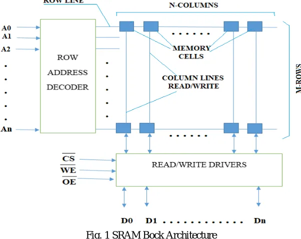
[image:2.612.155.456.148.387.2]Fig. 1 depicts architecture of SRAM block. It consists of M X N array of SRAM cells where M implies number of rows and N denotes number of columns. It also consists of row decoder and column decoder or read/write drivers. Here row decoder helps to select one among multiple words by activating appropriate address line.
Fig. 1 SRAM Bock Architecture
SRAM block has one or many memory cells which are in rectangular array form with some control circuitry to decode addresses for read and write operations. Each row contains M-cells and there are N-columns. Intersection of rows and columns contain a cell.
B. 6T SRAM
[image:2.612.121.500.500.667.2]As the name itself indicates the conventional 1-bit SRAM cell consists of 6 transistors, where the arrangement consists of two inverters which are connected back to back. The output of one inverter is fed back to the input for another one and vice-versa. There are two access transistors to facilitate read and write operation.
Fig. 2 Conventional 6T SRAM Cell
73
©IJRASET: All Rights are Reserved
1) Read Operation
a) Initially precharge the bit lines using precharge circuitry.
b) Activate word.
c) Based on the data which is stored at nodes Q and Qb the charging and discharging of bit-line capacitance takes place. Initially the capacitors are charged, if the value at node Q is 0 then the charge on bit-line BL gets discharged.
d) The sense amplifier used here senses the data bit by converting differential signal to logic level.
e) Finally word line is made low
2) Write Operation
a) Initially the word line is made low.
b) Both bit-lines are precharged to Vdd using precharge circuitry.
c) Word line is pulled high to activate access transistors.
d) The data and its complement are placed on bit-lines BL and BLB for writing.
e) Once Q and Qb overturns its state, word line is made low.
C. Peripheral Circuits
For successful read and write operation of SRAM memory, certain peripheral circuits are required they are:
1) Precharge circuit
2) Multiplexers for bit lines (BL and BLB) and
3) Sense amplifiers [2].
III.ADIABATICLOGIC
The term “Adiabatic” is derived from Greek word which signifies that it is impassable to heat. In other words no trade of heat between a system and the neighbouring environment. The fundamentals of adiabatic logic are as follows
1) When there is no voltage between the nodes, the switches are ON.
2) The switches are OFF, when there is no current passes through the node.
3) Use an active element that is able to recuperate the energy in the form of charge.
All the above fundamentals are attained by a time varying current source instead of a voltage source. Customarily, the designers underplay with the events, the node capacitances or the voltage swings to reduce the power waste [4].
Adiabatic switching circuits require non-constant, non-standard power supply with time-varying voltage. This power supply is known as “Pulsed power supplies” or “power clock”. These power supplies use circuit components capable of restoring the energy. Inverting the current supply causes the energy to flow from the load capacitance back into the power supply. So, the power supplies must be designed to retrieve the energy fed back to it.
A. Realization Of Power Clock
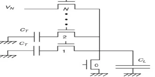
[image:3.612.185.444.581.710.2]The Fig. shown below helps to create power clock by charging the load capacitor in a stepwise manner using tank capacitors, the switches 1 to N are closed in an increasing order; here switches are applied to gate of the transistors and the steps may get vary from 2 to n-1. The charge at CL (load capacitor) vary from 0 to Vdd in steps of 0 to Vdd/n, Vdd /n to 2Vdd /n and so on. Practically overhead limitation of number of steps is 10.
74
©IJRASET: All Rights are Reserved
B. Realization of Adiabatic Gates
Adiabatic logic can be easily realized for any conventional CMOS logic by just replacing each pMOS and nMOS transistors in pull-up and pull-down networks with transmission gates (T-gates).
Since all the stimuli must be available in complementary form, both the networks in the adiabatic logic circuit are used to charge-up as well as charge-down the output capacitances. Expanded pull-up and pull-down networks to drive true and inverse output respectively[6].
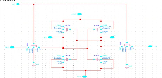
[image:4.612.51.561.196.343.2]Voltage source Vdd is replaced by a pulsed power supply with varying voltage to employ adiabatic operation. The pulsed power supply or the power clock is capable of recovering the energy back to source and hence reduces the power dissipation.
Fig 4. Conventional and Adiabatic Logic
IV.IMPLEMENTATION
All the implementations are done using ADE-L (Analog Design Environment) - which is an entry level design and simulation environment. It is product of cadence virtuoso. It is an industry leading task based environment for simulation and analysis of full custom RF design. It also has an inbuilt calculator with integrated waveform display. Here implementations are done using both 180nm and 45nm technology, however schematics of 180nm technology are given.
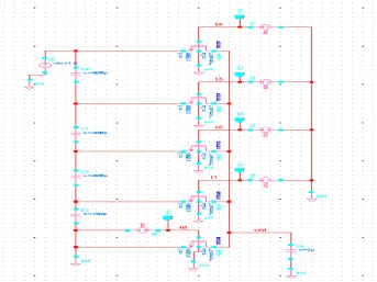
A. 6T SRAM
[image:4.612.46.574.459.714.2]75
©IJRASET: All Rights are Reserved
B. Peripheral Circuits
[image:5.612.164.499.145.337.2]1) Precharge Circuit: Precharge circuit is used to keep both bit lines in high state. The arrangement of precharge circuit is shown in Fig. 6. Here two PMOS transistors are connected in such a way that their source are connected to supply voltage and gates are connected as input as precharge, which acts as control stimuli for the circuit and both the drains of the transistor were connected to BL and BLB. The main objective of using precharge circuitry is to maintain uniformity of bit line voltages.
Fig. 6 Implementation of Precharge circuit
2) Multiplexers for BIT-lines(BL and BLB): Multiplexers are also important part in SRAM operation. It is one of the important circuitry during write operation. The Fig. 7 presents the schematic view of multiplexer circuits used for BL and BLB lines. The data to be written in cell is valid only when WE (Write Enable) signal is made high. Here in below configuration right multiplexer is connected to BL and left multiplexer is connected to BLB, it’s also connected in reverse fashion. The main difference exists between two multiplexers is, use of one additional inverter which is used to invert the data. The data and inverted data is were finally given to BL and BLB lines.
.
[image:5.612.90.512.442.718.2]76
©IJRASET: All Rights are Reserved
[image:6.612.161.481.117.324.2]3) Sense Amplifier: Sense amplifier is one of the important circuit during read operation, its objective is to sense small or low powered signal from bit lines to recognizable logic state such that the data can be interpreted easily. In this work a current mirror sense amplifier is used [4]. The schematic view of current mirror differential sense amplifier is shown in Fig 8.
Fig. 8 Implementation of Sense Amplifier
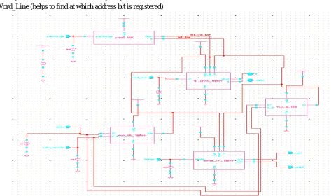
C. Single BIT Read and Write Operation
The single bit read and write operation were performed by merging all the peripheral circuits with SRAM. The below figure 9 shown is schematic view of single read write SRAM cell. The control signals given to schematic is as follows,
1) Precharge
2) Data (0 or 1)
3) Write_Enable (it gives access to write data into the memory cell)
4) Sense (verifies the bit stored in memory cell)
5) Word_Line (helps to find at which address bit is registered)
[image:6.612.64.537.441.721.2]77
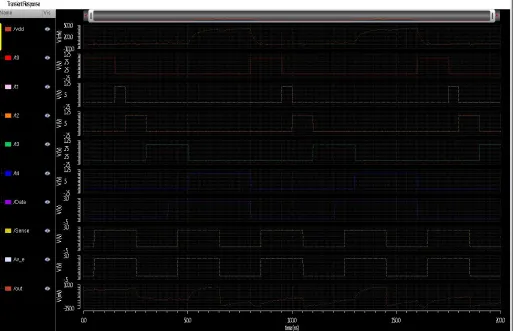
[image:7.612.75.565.76.392.2]©IJRASET: All Rights are Reserved
Fig. 10 Output Waveform for Conventional 6T SRAM
D. Implementation OF Power Clock Using Stepwise Charging Capacitor
This is an adiabatic way of generating power clock. Which is further applied to read write circuitry of SRAM cell for power reduction.
[image:7.612.142.485.453.710.2]78
©IJRASET: All Rights are Reserved
[image:8.612.46.561.82.347.2]E. Single Read and Write Operation of 6t Sram Using Adiabatic Logic
Fig. 12 Single Read and Write Operation of 6t SRAM Using Adiabatic Logic
[image:8.612.50.564.377.708.2]79
©IJRASET: All Rights are Reserved
V. RESULT
Performance analysis of different parameters using 180nm Technology.
Sl. No. Performance parameters Conventional SRAM Adiabatic SRAM
1. Static Power Consumption 420.4µW 198.81µW
2. Average Power 148.7µW 23.20µW
3. Peak Power 1640µW 616.3µW
4. Energy Consumption 73.40nW 16.29nW
5. Total Power Dissipation 82.38µW 13.42µW
6. Dynamic Power Consumption 338.02µW 185.39µW
Performance analysis of different parameters using 45nm Technology.
Sl. No. Performance parameters Conventional SRAM Adiabatic SRAM
1. Static Power Consumption 321.13µW 156.6µW
2. Average Power 66.60µW 42.74µW
3. Peak Power 129.1µW 85.1µW
4. Energy Consumption 50.27nW 8.56nW
5. Total Power Dissipation 60.67µW 38.94µW
6. Dynamic Power Consumption 260.46µW 117.66µW
VI.CONCLUSION
6T SRAM cell has been implemented using both conventional and adiabatic logic in 180nm and 45nm technology. The performance parameters like static power, dynamic power, peak power, average power, energy consumption, total power dissipation were evaluated using inbuilt calculator of cadence tool. We can observe that the power consumed by conventional SRAM is higher than that of adiabatic logic. Hence we can conclude that the circuits which mainly focus on low power consumption, adiabatic logic is the best choice.
REFERENCES
[1] Sung – Mo (Steve) Kang and Yusuf Leblebigi the authors of the book titled “CMOS Digital Integrated Circuits Analysis and Design, 3rd Edition published by Tata McGraw-Hill Education, New York, 2003.
[2] The authors Irina Vazir, Prabhjot S. Balaggan, Sumandeep Kaur and Cailan Shen, published paper on SRAM IP FOR DSP/SOC PROJECTS.
[3] Andrei Pavlov and Manoj Sachdev, the author of book CMOS SRAM Circuit Design and Parametric Test in Nano-Scaled Technologies Process – Aware SRAM Design and Test published by Springer Publications, 2008.
[4] Philip Teichmann, ADIABATIC LOGIC FUTURE TREND AND SYSTEM LEVEL PERSPECTIVE, Springer publications, 2012. [5] Jawar Singh, Saraju P.Mohanty and Dhiraj K. Pradhan, ROBUST SRAM DESIGNS AND ANALYSIS, Springer Publications, 2013
80
©IJRASET: All Rights are Reserved
BIOGRAPHIES
Irfan M. Trasgar received his B.E Degree (ECE) from Dr. AIT Bangalore, which is affiliated to VTU, Belagavi. Currently he is pursuing his postgraduate degree in M. Tech (VLSI Design and Embedded System) at K.L.E Dr. M S Sheshgiri College of Engineering and Technology, Belagavi. His research areas includes Embedded System, IoT and VLSI front and back end designing.
Dr Rajani H.P has received B.E Degree (ECE) from Karnataka University, Karnataka. She has obtained her M.Tech degree from N.I.T.K (K.R.E.C), Surathkal. She is currently heading the Department of Telecommunication Engineering at K.L.E Dr. M S Sheshgiri College of engineering and Technology, Belagavi. She has several publications in International Conferences and Journals. Her area of research includes design of low power CMOS circuits and Memories, Performance Improvement in CMOS circuits, Computer Organization, Embedded Systems etc. She has served as united member for Board of Studies (BOS), Member of Board of Examiners (BOE) and as visiting faculty at Visvesvaraya Technological University (VTU).
Suresh F. Murgod has received B.E Degree (ECE) from H R E C Nidasoshi. He has obtained his M.Tech degree (Electronics Engineering) from B M S College, Bangalore. Currently he is serving as a lecturer in E&C Department of K.L.E Dr. M S Sheshgiri College of Engineering and Technology Belagavi. His area of interest includes DSP, HDL coding for efficient utilization of FPGA resources, Embedded System.