LEABHARLANN CHOLAISTE NA TRIONOIDE, BAILE ATHA CLIATH TRINITY COLLEGE LIBRARY DUBLIN
OUscoil Atha Cliath The University of Dublin
Terms and Conditions of Use of Digitised Theses from Trinity College Library Dublin Copyright statement
All material supplied by Trinity College Library is protected by copyright (under the Copyright and Related Rights Act, 2000 as amended) and other relevant Intellectual Property Rights. By accessing and using a Digitised Thesis from Trinity College Library you acknowledge that all Intellectual Property Rights in any Works supplied are the sole and exclusive property of the copyright and/or other I PR holder. Specific copyright holders may not be explicitly identified. Use of materials from other sources within a thesis should not be construed as a claim over them.
A non-exclusive, non-transferable licence is hereby granted to those using or reproducing, in whole or in part, the material for valid purposes, providing the copyright owners are acknowledged using the normal conventions. Where specific permission to use material is required, this is identified and such permission must be sought from the copyright holder or agency cited.
Liability statement
By using a Digitised Thesis, I accept that Trinity College Dublin bears no legal responsibility for the accuracy, legality or comprehensiveness of materials contained within the thesis, and that Trinity College Dublin accepts no liability for indirect, consequential, or incidental, damages or losses arising from use of the thesis for whatever reason. Information located in a thesis may be subject to specific use constraints, details of which may not be explicitly described. It is the responsibility of potential and actual users to be aware of such constraints and to abide by them. By making use of material from a digitised thesis, you accept these copyright and disclaimer provisions. Where it is brought to the attention of Trinity College Library that there may be a breach of copyright or other restraint, it is the policy to withdraw or take down access to a thesis while the issue is being resolved.
Access Agreement
By using a Digitised Thesis from Trinity College Library you are bound by the following Terms & Conditions. Please read them carefully.
ELECTRONIC TRANSPORT AND
MAGNETIC PROPERTIES OF
ORGANIC SEMICONDUCTORS
Franklyn George Burke
School of Physics, Department of Scienee
University of Dublin
A thesis submitted to the University of Dublin in partial fulfilment of the
requirements for the degree of
Declaration
This thesis is submitted by the undersigned for examination for the degree Doctor of Philosophy at the University of Dublin. It has not been submitted as an exercise for a degree at any other university or degree issuing institution.
This thesis, apart from the advice, assistance and joint effort mentioned in the acknowledgements and in the text, is entirely my own work.
I agree that the library may lend or copy this thesis freely upon request.
J
TRINITY COLLEGE 1 9 JUL 20|1LIBRARY DUBLIN ^
-Summary
The primary aim of this research thesis is to investigate the electronic transport and magnetic properties of organic semiconducting materials. Undeniably, experimental and theoretical work is needed to conclusively study spin injection, transport and relaxation mechanisms in these types of materials. Currently, one of the major challenges that exist for organic spin electronic devices is the control and understanding of the ferromagnetic-organic interface. This lack of control is counterproductive in achieving tuneable devices with substantial reliability. In order to adequately attend to this lack of control, considerable care must be taken to fabricate organic devices with precise dimensions while maintaining reproducible material quality. If these relevant parameters are accurately tuned with an acceptable tolerance level, a wealth of information can be obtained about spin transport in these devices. The main approach of this thesis was to systematically explore the temperature and magnetic field dependence of spin electronic transport of both crystalline and amorphous organic materials incorporating various spin injecting electrodes along with unique structural configurations.
Electronic spin-polarized transport devices were fabricated using molecular
semiconducting nanowires, micro-crystals and amorphous thin films with metallic electrodes patterned by photolithography, electron beam lithography and shadow masks. These organic materials were either grown by vapour transport, synthesis or thermal evaporation. To gain a better understanding of the molecular structure of these materials that influence electron transport, structurally analysis was also performed using both destructive and non-destructive techniques. This thesis describes in detail the various techniques used as well as the distinct features that each material possess. Temperature dependent electronic tran.sport and
magnetoresistance were observed in various materials with different structural properties. Various experimental analyses were performed in order to shed some light on the possible contributions responsible for electron injection at the metal/organic interface. The work performed in this thesis will also help to provide a better understanding of the critical
mechanisms that are responsible for spin-transport in organic materials from an experimental physics point of view.
Acknowledgements
First and foremost I would like to thank Prof. J.M.D. Coey for providing me with the opportunity to work in his research group, for his professional guidance over the past few years and for creating a good environment for me to develop as a skilled researcher. Enormous thanks must be given to Dr. Mohamed Abid and Dr. Plamen Stamenov for their assistance in finding unique solutions for unique technical problems. Many thanks should also be given to Dr. M. Venkatesan and Dr. Lorena Monzon for their help with magnetization measurements and molecular synthesis, respectively. I would like to also thank Prof. Greg Szuiczewski for sharing his knowledge of organic materials. Special thanks must be given to Mr. Peter Gleeson from Intel for his help with the EBL process.
Thanks to all the past and present members of the research group for their advice and support. In alphabetical order: Adriele, Cathy, Chris, Ciaran, Damaris, Darragh, Fiona, Gabriela, Gen, Greg, Guoqiang, Huseyin K., Fluseyin T., Jiafeng, Jonathan, Kaan, Karl, Karsten, Lorenzo, Marita, Matt, Mazhar, Milena, Peter, Robbie, Sebastiaan, Simone, Xu, Zhu. The technical and administrative staff at CRANN also deserves a special thanks for their support over the years.
Table of Contents
Introduction... 1
1.1 Background... I 1.2 Organic Semiconductors and Electronics... 2
1.3 Charge Transport in Organic Materials... 5
1.3.1 Band Transport... 8
1.3.2 Hopping Transport... 9
1.3.3 Space Charge Limited Currents (SCLC)... 12
1.4 Organic Spin Electronics... 15
1.5 Organic Spin-Valves and Magnetoresistance...26
1.6 References...28
Experimental Techniques... 33
2.1 Introduction...33
2.2 Absorbent-Assisted Physical Vapor Transport...33
2.3 Organic Thermal Evaporation... 35
2.4 Shamrock Sputtering System... 36
2.5 EEI FIB Dual Beam Strata System...39
2.6 Photo-Lithography...40
2.7 X-ray Analysis... 41
2.8 Transmission Electron Microscopy(TEM)... 43
2.9 Superconducting Quantum Interference Device (SQUID)...44
2.10 Physical Property Measurement System (PPMS)... 45
2.11 Millatron System...46
2.12 Resistivity-Temperature Rig (RT-rig)... 47
2.13 Atomic Force Microscope (AFM)...48
2.14 BOC Edwards Evaporator Auto 500... 49
2.15 References... 50
Al-doped 8-hydroxyquinoline Wires and Alq3 Thin Film... 5 1 3.1 Introduction... 51
3.2 Al-doped 8-hydroxyquinoline Single Crystalline Wires...52
3.3 Magnetic Properties of Al-dopcd 8-hydroxyquinoline Wires... 61
3.4 Fabrication and Characterization of Organic Nano-wire Structures...63
3.5 Alq3 Thin Film... 70
3.6 Magnetization of CoFe/Alq3 and Co/Alq3 Bilayers... 76
3.7 References...83
Bis-(8-hydroxyquinoline) Metal (II) Materials... 85
4.1 Introduction...85
4.2 Characterization of Bis-(8-hydroxyquinoline) Metal (II) Materials...86
4.3 Magnetic Properties of Mq2 Materials... 99
4.4 Electronic Transport Properties of Mq2 Based Devices... 109
4.5 References... 113
Rubrene Single-Crystals...115
5.1 Introduction... 115
5.2 Properties of Rubrene Crystals... 117
5.3 Lateral Rubrene Crystal Based Devices... 122
5.5 References... 151
Ceo Nanorods... 153
6.1 Introduction... 153
6.2 Fabrication of Ceo Nanorods... 154
6.3 Lateral C6o Nanorod-Based Devices... 156
6.4 References... 164
Hexathiapentacene (HTP) Crystals and Pentacene Thin Films... 166
7.1 Introduction... 166
7.2 Hexathiapentacene (HTP) Crystals... 167
7.3 Lateral HTP Based Devices... 170
7.4 Pentacene Thin Films... 180
7.5 Pentacene Thin Film Based Devices... 182
7.6 References... 190
Conclusions and Future Work... 193
List of Figures
Figure 1.1: Schematic of GMR device configuration; a) parallel b) anti-parallel
Figure 1.2: Band diagram sketch of device structure [60|: model consists of two FM metal contacts with resistive interface layer sandwiching a semiconductor. The quasi-Fermi levels for the charge carriers, a) parallel polarization b) anti parallel polarization
Figure 2.1; Schematic of ab.sorbent-assistcd physical vapor transport setup Figure 2.2: Organic thermal evaporator
Figure 2.3: Side-view schematic of organic evaporator (Reprinted from Sigma Instruments Manual [3].)
Figure 2.4: Shamrock sputtering system
Figure 2.5; Top view schematic of Shamrock sputtering system
Figure 2.6: a) TFT gun with shutter b) DC clusters with independent shutters Figure 2.7: a) Ion milling gun b) Substrate heater
Figure 2.8: FEI FIB Dual Beam Strata System
Figure 2.9: Kliendiek micromanipulator mounted inside FEI system Figure 2.10: Class 100 clean room with mask aligner and wet bench Figure 2.1 I: Panalytical X’Pert Pro X-ray Diffractometer
Figure 2.12; Experimental setup for x-ray analysis Eigure 2.13: SQUID magnetometer system
Eigure 2.14: Quantum Design Physical Property Measurement System Eigure 2.15: Millatron system
Figure 2.16 a) Resistivity-temperature rig (RT-rig) system b) Sample box in the center of the magnetic field for measurement at 300 K c) Sample mounted on the crygenic head.
Figure 2.17: Asylum atomic force microscopy (AFM) system (Reprinted from Asylum Research AFM Manual[4])
Figure 2.18: BOC Edwards Evaporator Auto 500 system
Figure 3.1: Preliminary Analysis of Al-doped organic wires: a) SEM image, b) TEM image with diffraction pattern c) ETIR spectra.
Figure 3.3: Figure 3.4: Figure 3.5: Figure 3.6: Figure 3.7: Figure 3.8: Figure 3.9: Figure 3.10: Figure 3.11: Figure 3.12: Figure 3.13: Figure 3.14: Figure 3.15: Figure 3.16: Figure 3.17: Figure 3.18: Figure 3.19: Figure 3.20: Figure 3.21: Figure 3.22: Figure 3.23: Figure 3.24: Figure 3.25: Figure 3.26:
XRD patterns: a) Al-doped 8-hydroxyquinoline wires and Alq3 powder comparison b) Al-doped 8-hydroxyquinoline wires on different systems. TGA plots of Alq3 powder, 8-hydroxyquinoline wires and Al-doped 8- hydroxyquinoline wires.
TGA and first derivative TGA plots of the Al-doped 8-hydroxyquinoline wires. TGA and first derivative TGA plots of the Alq3 powder.
NMR plots of Alq3 powder, Al-doped and 8-hydroxyquinoline wires. SEM image of micro-scale Al-doped wire on patterned Au pads. EDX elemental mapping images of Al-doped 8-hydroxyquinoline wire. Conglomerated EDX elemental mapping image of Al-doped 8-
hydroxyquinoline wire on pattern Au pad.
Magnetization curves of Alq3 powder: a) M vs. H curves b) M vs. T curves. Magnetization curves for Al-doped wires: a) M vs. H curves b) M vs. T curves EPR signal of Al-doped wires at different temperatures.
SEM images: a) Top view of patterned electrodes b) Al-doped wire secured across a 120 nm gap.
I-V and dl/dV curves of NiFe/AI-doped Wire (120 nm)/NiEe device. Transport measurements for NiFe/AI-dopcd Wire (120 nm)/NiFe device: a) Resistivity vs. T curves b) MR curves.
Tran.sport measurements for Au/AI-doped Wire (I20nm)/Au device: a) 1-V curves b) MR curves.
Transport measurements of NiFe/AI-doped Wire (400 nm)/NiFe: a)MR curves at various temperatures b)Resistivity vs. temperature curves.
Transport measurements of NiFe/AI-doped Wire (700nm)/NiFe: a)MR curves at various temperatures b)Resistivity vs. temperature curves.
AFM image of Alq3 thin film grown on Si()2 substrate. FTIR spectra of as grown Alq3 thin film
Raman spectra of the Alq3 thin film grown on a Si substrate. UV-vis absorption spectra of Alq3 thin film on glass slide
Figure 3.27: a) Magnetization curves of CoFe films grown on Si/Si()2 substrates after diamagnetic correction b) Magnetic moment vs. CoFe thickness with linear fit illustrating the thickness of the dead layer.
Figure 3.28: a) Magnetization curves of CoFe films grown on Si/Si()2/Alq3(40nm) substrates after diamagnetic correction b) Magnetic moment vs. CoFe thickness with linear fit illustrating the thickness of the dead layer. Figure 3.29: a) Magnetization curves of 2nm CoFe film grown on Si/Si02 substrate at
various temperatures before diamagnetic correction.
Figure 3.30: a) Magnetization curves of Co films grown on Si substrates after diamagnetic correction b) Magnetic moment vs. Co thickness with linear fit illustrating the thickness of the dead layer.
Figure 3.31: a) Magnetization curves of Co films grown on Si substrates coated with 40nm thick Alqi film |Si/Co/Alq3(40nm)] after diamagnetic correction b) Magnetic moment vs. Co thickness with linear fit illustrating the thickness of the dead layer.
Figure 3.32: a) Magnetization curves of Co films grown on Si/Alq^ (40nm) substrates lSi/Alq3(4()nm)/Col after diamagnetic correction b) Magnetic moment vs. Co thickness with linear fit illustrating the thickness of the dead layer.
Figure 3.33: TEM images of 9 nm Co film grown on Si substrate coated with 40 nm thick Alq3 film, a) View of entire stack, b) Closer view of Co/Alq3 interface. Figure 4.1: Molecular structure of Znq2 molecule (reprinted from [ 16|)
Figure 4.2: AFM images of bis-(8-hydroxyquinoline)metal(Il) thin films on Si02 substrates with I x I pm" .scan area a)Mnq2, b)Coq2, c)Feq2, d)Znq2, c)Niq2, and f) Cuq2.
Figure 4.3: EDX spectrum of bis-(8-hydroxyquinoline)metal(II) thin films on Si()2 substrates a) Coq2, b) Feq2, c) Mnq2, and d) Niq2
Eigurc 4.4: EDX spectrum of bis-(8-hydroxyquinolinc)metal(II) thin films on Si()2 substrates a) Znq2,and b) Cuq2.
Figure 4.5: UV-vis absorption spectra of bis-(8-hydroxyquinoline)metal(II) molecules in DMSO solution.
Figure 4.6: Maximum wavelength (Zmax) vs. Ionic radii M^"^ high spin (ppm) obtained from UV-vis absorption spectra of bis-(8-
hydroxyquinoline)metal(II)molecules.
Figure 4.7: UV-vis absorption spectra of bis-(8-hydroxyquinoline)metal(II) thin films on glass slide.
Figure 4.8: PL spectra of Znq2 thin film grown on a Si02 substrate.
Figure 4.11: X-ray diffraction patterns of Mnq2, Feq2, Coq2, Niq2 and Znq2 thin films on SiOT substrate.
Figure 4.12: X-ray diffraction patterns of Cuq2 thin film and powder on Si02 substrate. Figured. 13: Molar susceptibility vs. temperature of bis-(8-hydroxyquinoline)metal(II)
powders with the reciprocal molar susceptibility in the inset.
Figure 4.14: Reciprocal molar susceptibility vs. temperature of bis-(8-hydroxyquinoline) metal(II) powders.
Figure 4.15: EPR signal of Mnq2 powder at room temperature.
Figure 4.16: Magnetization curves for Coq2 thin film: a) M vs. H curves at 300 K and 4 K with a magnified view in the inset b) M vs. T curves at IT with a linear fit of
1/X vs. T curve in the inset.
Figure 4.17: Magnetization curves for Feq? thin film: a) M vs. FI curves at 300 K and 4 K with a magnified view in the inset b) M vs. T curves at IT with a linear fit of
1/X vs. T curve in the inset.
Figure 4.18: Magnetization curves for Mnq2 thin film: a) M vs. H curves at 300 K and 4 K with a magnified view in the inset b) M vs. T curves at IT with a linear fit of l/X vs. T curve in the inset.
Figure 4.19: Magnetization curves for Niq2 thin film: a) M vs. H curves at 300 K and 4 K with a magnified view in the in.set b) M vs. T curves at IT with a linear fit of
1/X vs. T curve in the inset.
Figure 4.20: Magnetization curves for Znq2 thin film: a) M vs. H curves at 300 K and 4 Kb) M vs. T curves at I T.
Figure 4.21: Schematic of vertical multilayer Mq2 based thin film structures.
Figure 4.22: Current vs. voltage curves of bis-(8-hydroxyquinolinc)metal(II) based vertical structures with Ag electrodes.
Figure 4.23: Schematic band diagram of Ag/Mq2/Ag interfaces
Figure 5.1: Evolution of field effect mobility of OFETs (reprinted from Y. Iwasa, et. al. (51)
Figure 5.2: Schematics showing standard approaches used for the fabrication of rubrenc crystal based FETs [5].
Figure 5.3: Molecular structure of rubrene (reprinted from T. Hasegawa et. al. [9]) Figure 5.4: Schematic of absorbent-assisted physical vapour transport setup.
Figure 5.5: SEM images of rubrene based organic particles on Si02 substrate created by AA-PVT a)150 x I50um view b) 10 x 10pm view.
Figure 5.7: AFM images of rubrene crystal lop surface a) 5 x 5 pm .scan b) I x 1 pm .scan
Figure 5.8: Profile of molecular step on rubrene crystal surface
Figure 5.9: X-ray diffraction patterns of rubrene powder and micro-crystals on silicon substrates. Inset: SEM image of rubrene powder.
Figure 5. It): X-ray Diffraction pattern (Rigaku Saturn 724) of rubrene single crystal. Inset: EDX pattern.
Eigure 5.11: Stacking of rubrene molecular structure in a crystal (reprinted from T. Hasegawa et. al. [9])
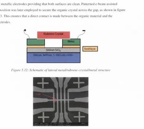
Figure 5.12: Schematic of lateral metal/rubrene-crystal/metal structure
Figure 5.13: SEM image of metallic electrodes after EIB milling of gaps
Eigure 5.14: SEM image of rubrene crystal across a 280 nm gap of Au electrodes
Eigure 5.15: I-V curves of lateral Au/Rubrene/Au structure al various temperatures. Inset: I-V at 70 K to 10 V.
Figure 5.16: Resistance vs. temperature curve of lateral Au/Rubrene/Au structure at 1V bias
Figure 5.17: SEM image of Rubrene crystal across a 300 nm gap of NiEe electrodes
Figure 5.18: I-V curves of lateral NiFe/Rubrene/NiFe structure at various temperatures. Inset: I-V at 70 K to 10 V.
Figure 5.19: Resistance vs. temperature curve of lateral NiFe/Rubrcnc/NiFe structure at 1 V bias.
Figure 5.20: Conductivity (o) vs. temperature (K) curve of lateral NiFc/Rubrene/NiFc structure.
Figure 5.21: Resistance vs. magnetic field (T) of lateral NiFc/Rubrene/NiFe structure at 80K
Figure 5.22: Resistance vs. magnetic field (T) of lateral NiFe/Rubrene/NiFe structure at 70K.
Figure 5.23: Resistance vs. magnetic field (T) curves of lateral NiFe/Rubrene/NiFe structure at different temperatures.
Figure 5.24: Magnetoresistance vs. temperature curve of lateral NiFe/Rubrene/NiFe structure at IV bias.
Figure 5.25: SEM image of lateral NiFe/Rubrene/NiEe structure with a 273 nm gap.
Figure 5.26: I-V curves of lateral NiFe/Rubrene/NiFe structure at various temperatures.
Figure 5.27: Logarithmic 1-V curves of lateral NiEe/Rubrene/NiFe structure at various temperatures.
Figure 5.29: Differential Conductance/I-V curves of NiFe/Rubrene/NiFe structure at various temperatures a) 300K b) 230K c) 155K d) lOK.
Figure 5.30: SEM image of CoFe/Rubrene/CoFe structure with a 203 nm separation between the CoFe electrodes.
Figure 5.31: I-V curves of lateral CoFe/Rubrene/CoFe structure at various temperatures. Inset: Logarithmic I-V curves.
Figure 5.32: Logarithmic conductivity (a) vs. inverse temperature (K) curve of lateral CoFe/Rubrene/CoFe structure. Inset: Resistance vs. temperature curve.
Figure 5.33: SEM image of lateral CoFe/AlOx/Rubrene/AKVCoFe structure with a 280nm separation between the electrodes.
Figure 5.34: I-V curves of lateral CoFe/AlOx/Rubrene/AIOx/CoFe structure at various temperatures.
Figure 5.35: Logarithmic I-V curves of lateral CoFe/AlOx/Rubrene/AKVCoFe structure at various temperatures.
Figure 5.36: Logarithmic conductivity (o) vs. inverse temperature (K) curve of
CoFe/AIOx/Rubrene/AlOx/CoFe structure. Inset: Resistance vs. temperature curve.
Figure 5.37: Normalized Differential Conductance/I-V curves of
CoFe/AlOx/Rubrenc/AIOx/CoFe structure at various temperatures a) 300K b) 230Kc) 2]0Kd) I OK.
Figure 5.38: Schematic of rubrene crystal FET on MgO/Co source/drain electrodes a) Cross-sectional view b) Top-view.
Eigure 5.39: SEM image of lateral Co/MgO/Rubrene/MgO/Co with a 1pm gap.
Eigure 5.40: Drain current vs. drain voltage curves at different gate voltage biases of lateral Co/MgO/Rubrene/MgO/Co structure.
Figure 5.41: A magnified view of the Drain current vs. drain voltage curves at different gate voltage biases of lateral Co/MgO/Rubrene/MgO/Co structure.
Figure 5.42: Schematic of rubrene crystal FET with tungsten source/drain electrodes and SiCT gate dielectric.
Eigure 5.43: Drain current vs. drain voltage curves at different gate voltage biases of
rubrene crystal with tungsten electrodes on Si02 gate dielectric, a) Asymmetric curves b) Magnified view of the negative bias region of the curves.
Eigure 5.44: Drain current vs. gate voltage curves at different drain voltage biases of
rubrene crystal with tungsten electrodes on Si02 gate dielectric, a) Asymmetric curves b) Magnified view of the negative bias region of the curves.
Figure 5.46: Drain current vs. drain voltage curves at different gate voltage biases of rubrene crystal with tungsten electrodes on PMMA/Si02 gate dielectric. Figure 5.47: Drain current vs. gate voltage curves at different drain voltage biases of
rubrene crystal with tungsten electrodes on PMMA/Si()2 gate dielectric. Figure 6.1: a) Schematic Ceo molecular structure b) SEM image of a single Ceo rod on
silicon substrate
Figure 6.2: TEM images of single crystal Cgo rods on carbon grid a) Image of several Cao rods with EET pattern in the inset, b) Image of segments of Cao rods at higher magnification c) HRTEM Image of the tip of one Cao rod. d) HRTEM Image of the edge of one Cao rod.
Figure 6.3: SEM images of lateral single crystal Cao device a) Image of Cao rods with Pt electrodes, b) Image of Cao rods with Au electrodes secured by Pt wire.
Eigure 6.4: Resistance vs. Temperature of lateral single crystal Cao devices with Au and Pt electrodes
Figure 6.5: SEM images of lateral single crystal Cao device with CoFe electrodes Eigure 6.6: Current vs. Voltage curves of lateral crystal Cao device with CoEe electrodes
measured at various magnetic fields.
Figure 6.7: Current vs. magnetic field (T) curve of lateral single crystal Cao-CoFe device with an applied bias of 24 V.
Figure 6.8: Current vs. magnetic field (T) curve of lateral single crystal Cao-CoFe device with an applied bias of 25 V.
Figure 6.9: Current vs. magnetic field (T) curve of lateral single crystal Cao-CoFe device with an applied bias of 27 V.
Figure 6.10: Magnetocurrent(%) vs. Bias voltage plot of lateral single crystal Cao-CoFe device at 1.8 K.
Figure 7.1: Schematic of the crystal structure illustrating the synthesis of the HTP molecule via the combination of pentacene and sulphur.
Figure 7.2: SEM image of HTP wires on a silicon substrate
Figure 7.3: TEM images of single crystal HTP nanowires on carbon grid a) Image of several nanowires, b) Image of segment of a single nanowire displaying the tip of the wire, c) HRTEM Image of the side of a nanowire, d) HRTEM Image of the edge of a nanowire with diffraction pattern in the inset.
Figure 7.4: SEM image of single crystal HTP nanowire with Pd electrodes.
Eigure 7.5: Current vs. Voltage curves of single crystal HTP nanowire with Pd electrodes measured at different temperatures.
Figure 7.7: Current vs. Voltage curves oF lateral crystal HTP_CoFe_l device measured at different temperatures.
Figure 7.8: Resistance vs. Temperature curves of lateral crystal HTP device with CoFe electrodes measured with and without magnetic field.
Figure 7.9: Logarithmic conductance vs. inverse temperature curve of lateral crystal HTP device with CoFe electrode measured at zero magnetic field.
Figure 7.10: Resistance vs. magnetic field (T) curve of lateral single crystal HTP-CoFe device with an applied bias of 50nA.
Figure 7.11: SEM image of HTP_CoFe_2 device with a 400nm gap between electrodes.
Figure 7.12: Current vs. Voltage curves of the HTP_CoFe_2 device measured at different temperatures.
Figure 7.13: Resistance vs. Temperature curves of HTP_CoFe_2 device measured at different magnetic fields.
Figure 7.14: Resistance vs. magnetic field (T) curves for the HTP_CoFe_2 device at lOK and 20K.
Figure 7.15: Resistance vs. magnetic field (T) curves for HTP_CoFe_l and HTP_CoFe_2 devices at I OK.
Figure 7.16: AFM images of crystalline pentacene thin film on oxidized silicon substrate 2 2
a) Image of 5x5pm area b) Image of 1 x 1 pm area.
Figure 7.17: XRI) pattern of pentacene thin film and powder on an oxidized silicon substrate.
Figure 7.18: a) Cross sectional view of Si membrane sandwiched by Si02 insulators, b) SEM image of Si membrane with Ga+ ion milled patterns for the shadow mask for the electrodes.
Figure 7.19: SEM images of ALO.VCo/Ag electrodes deposited on top of pentacene film a) Top view of the entire structure b) View of the separation between the two electrodes.
Figure 7.20: Schematic of pentacene film structure with spin polarized top contact electrodes a) Cross sectional view b) Top view.
Figure 7.21: SEM image of pentacene film structure with top contacts after being contacted by e-beam assisted deposition of platinum wires.
Figure 7.22: Current vs. voltage curves of pentacene film structure with top contacts measured at various temperatures. Logarithmic plot is shown in the inset.
Figure 7.23: Resistance vs. temperature curves of the pentacene film with top contacts measured at bias voltages 0. IV and 0.2V.
view of the IV curves at higher biases and the measured resistance vs. magnetic field.
Figure 7.25: SEM images of bottom contacting .source/drain electrodes a) Image of Si- membrane with Ga-i- ion milled pattern for shadow mask of asymmetric electrodes, b) Image of deposited spin polarized electrodes oxidized silicon substrate.
Figure 7.26: SEM images of fabricated bottom contacting source/drain electrodes a) Image of electrodes contacted by Ag pads, b) Close-up image of asymmetric spin polarized electrodes.
Schematic of cross sectional view of pentacene FET with spin polarized bottom contacted source/drain electrodes.
Figure 7.27:
List of Tables
Table 3.1: Composition of Al-doped wires and Alq3 powder.
Table 4.1: Summary of measured maximum wavelength and HOMO-LUMO gap of bis-(8- hydroxyquinoline)metal(II) molecules.
Table 4.2: Summary of measured and extracted magnetic parameters of Mq2 powders. Table 4.3: Summary of measured and extracted magnetic parameters of Mq2 films. Table 5.1: Summary of critical parameters associated with rubrene-based devices with
Chapter 1
Introduction
1.1 Background
The unification of spin-electronics and organic electronics has emerged as one of the most promising fields of research in recent times. Several academic and industrial
laboratories have embraced the basic idea of guiding or manipulating spin-polarized electrons through an organic medium. This new area of research has been often referred to as organic spinlronics [11. Employing organic materials as a transport medium offers several advantages. Weak intermolecular bonds present in these materials permits the creation of a wide range of structurally tlexible devices which can be incorporated into various applications such as displays. Organic systems can easily be chemically synthesized using countless techniques at a very low cost compared to inorganic systems. This also opens the pathway for the
fabrication of low-weight, versatile electronic devices. The use of organic electronics has grown tremendously over the last decade with the emergence of organic light-emitting diodes (OLEDs) [2]. Companies such as Philips, Kodak and Pioneer have successfully incorporated them as displays in products such as mobile phones, digital cameras and automobiles. Other firms are researching novel solutions for realizing organic-based transistors, solar cells, sensors and lasers. With this in mind, it has long been predicted that OLEDs will capture a significant portion of the display market mainly due to the fact that inorganic light-emitting diodes (LEDs) remain fairly expensive to fabricate in comparison |3]. In order to truly realize this forecast, the efficiency of these devices would need to improve to nearly 100%.
holes transporting through a solid. Whenever a photon is absorbed into a solid an exciton is created. An cxciton is commonly referred to as a bound state of an electron and a hole. During a typical operating state of an OLED triplet are approximately 75% of the excitons formed, while the other 25% are spin-singlets which radiatively combine to emit photons. Consequently, the maximum efficiency is restricted to only 25% because the non-radiative recombination of the triplets produces phonons and do not contribute to the overall emission of light (4J. In order to improve the efficiency of these devices with the incorporation of ferromagnetic electrodes, a clear understanding of the relevant spin relaxation mechanisms acting upon spin transport through organic materials is needed. This sets the foundation for the primary objective of this research project, which intends to study issues relating to spin injection, transport, and relaxation. Specifically recognizing the key mechanisms which are responsible for spin relaxation in organic semiconductors whether they are intrinsic or extrinsic.
1.2 Organic Semiconductors and Electronics
The earliest application for organic materials in electronics was as electrical insulation or as a dielectric material, where it was mainly used to support or separate electrical conductors from each other in capacitors (2j. As characterization techniques improved over the years, the unique electrical and optical properties of these organic materials were realized. In general, there are several types of organic semiconductors: small molecules, oligomers (short chain), polymers (long chain), etc. Conductivity in organic semiconductors is facilitated by several types of carriers depending on the material. In the case of molecules with ;r-conjugated systems, electrons travel via overlapping ;r-electron clouds. The core of many of these small molecules are created from the o-bonds which are stronger compared to these Ti-bonds [2]. Delocalization can occur in molecular systems when 7t-electrons overlap between adjacent carbon atoms. The p-orbital overlap between adjacent molecules depends on the orientation of the molecules. The bandgap which is normally in the range of 1.5 to 5eV is determined by the extent of this overlap.
compounds like ethylene (C2H2), each carbon atom is separated from its neighbor by three o bonds and a tt bond. In the case of molecules like benzene, the delocalization of the n electrons causes the extension of the orbitals around the molecule and further reduces the energy gap between the highest occupied molecular orbital (HOMO) and the lowest unoccupied molecular orbital (LUMO). The electron configuration of a single carbon atom (I s'2s^2p") has the capacity to bond with other carbon atoms and therefore creating a variety of molecular orbitals due to the modification of the electron wavefunctions. In the situation where long chains of carbon atoms exists, like in poly-para-phenylene-vinylene (PPV), a ID electronic system is created due to the delocalization of n bonds along the chain [5], The injection and transport of charge carriers in this system is mainly restricted by the transfer of electrons between molecular chains since the orbital molecular overlap is very low. In small molecules organics like tris-(8-hydroxyquinoline) aluminum (Alq3) the electron are
delocalized on the molecule but the transfer of electrons between molecules is related to the intermolecular separation.
In the event of bonding between two carbon atoms, Is orbitals are not altered but the wavefunctions associated with the 2s orbitals interact with two of the three 2p orbitals
2 creating a level of electron configuration. At a 120° angle relative to each other, the three sp orbitals lie on the molecular plane with the remaining p orbital orthogonal to the molecular plane. Additional molecular bonds can be made with these exposed hybrid sp" orbitals. Strong covalent bonds are typically made on the molecular plane, while weak covalent bonds are made orthogonal to the molecular plane. The weak bonds contribute significantly to the conductivity of the molecule due to the formation of delocalized electron density orthogonal to the molecular plane and a path for charge carriers to travel [5).
presenting some interesting challenges in integrating these materials into existing device
fabrication processes, in order not to decompose or alter the material in any way. Electrically,
a charge carrier propagating through the material can locally distort the bonds since the forces
are so weak. This type of distortion along with the carrier can be considered as a quasi
particle commonly referred to as a polaron, which only carries a half spin, A polaron is made
up of an electron with an associated local structural distortion. If two of these polarons are
close together then they form a bipolaron and enter a singlet state and will not have spin
associated with them [7],
Charge carrier transport in organic semiconductors can be described by either band or
hopping transport depending on the degree of order of the material. Highly pure molecular
crystals tend to conform to band transport. The carrier mobility at room temperature in these
crystals is in the range of 1 to 35 cm fVs [8] which is significantly less than that of crystalline
silicon. Temperature tends to play a crucial role during transport to the extent that there is a
power law dependence of the mobility. Essentially, the increase in temperature causes an
increase in thermal agitation of the semiconductor atoms, which results in an increase in the
lattice scattering [2]. The power law behaviour seen in the mobility as the temperature
decreases is denoted by n which represents the rate of decay in temperature.
^ oc T " with n = 1 ...3 (1.1)
Hopping transport dominates in amorphous organic solids with a carrier mobility of
typically lO'^’cm^A's or less. Hopping tends to occur between localized molecular states. In
this case, the mobility depends strongly on applied electric field (F) and temperature as seen
in the following relationship [2, 9],
jU{F,T) oc e\pi-AFIkgT) expi^fi-iF Ik^T) (1.2)
The electric field and temperature dependence of the carrier mobility fits directly with
the well established Gaussian Disorder Model (GDM) proposed by Bassler in order to
represent charge transport mechanisms in many amorphous organic materials [9], The model
views the organic material as a collection of transport sites for hopping conduction, while
each molecule represents a transport site for charge carriers. Each site is unique with their
own random potential energies and distances in relation to each other. Charge hopping is
For both pure crystalline and amorphous organic materials, trapping effects alter the normal behavior of these materials during transport. To date, organic thin films such as thieno[3,2-b] thiophene have demonstrated similar carrier mobility to amorphous silicon (1 cm /V s), but not anywhere near to the mobility achieved in crystalline silicon 110]. There is a similar story for the charge carrier density of organic semiconductors, where the magnitude of free charge carriers is several times larger in silicon. A shortage of free charge carriers translates into very low conductivity if the organic material is very pure, but this can be improved by controlled doping using similar methods such as electro-chemical and field-effect doping, as exploited in the microelectronics industry. This process has not proved to be as straight forward as it might seem due to the fact that the purity of organic semiconductors is not nearly as high as extrinsic inorganic semiconductors so precision doping is very difficult. In addition, organic semiconductors with a relatively low free charge density find it challenging to ionize dopants. On the other hand, ultra-pure single crystal organic materials like rubrene and pentacene have exhibited reproducible electrical properties with electric mobilities reaching 20 cmVVs and 3.5 cm'/Vs, respectively at room temperature [8, 11 ].
The injection of carriers across a typical metal-organic interface is governed heavily by the energy barrier height and the density of states at the Fermi level of the contacting metal and the organic material. Mismatch of the FIOMO or LUMO levels of an organic
semiconductor in reference to the work function of a metallic electrode can lead to a relatively high contact resistance. The Schottky barrier created at the interface results in a non-linear current-voltage (I-V) curve as seen in diodes. This has prompted researchers to incorporate metals such as aluminum and calcium with significantly lower work function to suppress the interface effects.
1.3 Charge Transport in Organic Materials
Charge-transport in conjugated materials depends heavily on the packing of the
strong interactions of small polarons with defects. These defects which have various origins and charge energies are known to produce localized electronic states in the HOMO-LUMO gap. Deep traps occur if the energy difference between the localized states and the mobility edge (energy which divides localized from extended states) is greater than keT. In the event of a deep trap situation thermal excitation cannot liberate the charge. When the energies associated with these localized states are less than keT, they are referred to as shallow traps with a finite trapping time [13J. In a standard OFET, the threshold voltage depends a great deal on the overall density of deep traps illustrated below
yth _ eN Deep Trap
C, (1.3)
The drifting of the trap states closer to the band edge with decreasing temperature exposes the strong temperature dependence of these deep traps.
The influence of traps on electronic transport is evident, but determining whether or not the observed electrical characteristic in a particular organic material is mainly due to the intrinsic properties of the material or is trap-dominated is not trivial. The common consensus is that all field-induced carriers can contribute to electron transport providing that the carrier density threshold is reached and there is an obvious decline in mobility compared to a trap-free system.
The electronic properties of small molecule organic semiconducting materials arc determined by the structure of an isolated molecule due to the fact that weak van der Waals bonding forces result in a weak intermolecular overlap of electronic orbitals which in turn causes the electronic bands to be narrow and exhibit electron-lattice coupling. The low symmetry of molecular packing in organic molecular structures is directly related to the anisotropy of the transfer integrals between adjacent molecules.
reduced the mobility is suppressed since charge transport in this regime is dominated by traps [ 13|. The herringbone packing of the molecules in these crystals tends to stack along the b- axis essentially orienting the charge transport along the ordered direction of the stack.
The intrinsic transport properties of these organic crystals can also be investigated using Hall Effect measurements, where the difference in electrical potential measured across the semiconducting channel is induced by an external perpendicular magnetic field. This effect is possible due to the fact that a charge carrier that moves through the channel in the presence of a transverse magnetic field is affected by a Lorentz force. It is believed that the trapped carriers are impervious to the Lorentz force and do not contribute to the Hall voltage, so the observed Hall Effect is intrinsic in nature 117]. These Hall Effect experiments revealed that charge transport occurred on the surface of the crystal via delocalized states over a significant temperature range.
In the case of an OEET device with p-type conductivity, the injection of holes through a interfacial Schottky barrier depends heavily on the work function of the metal, electron affinity of the semiconductor and the interfacial dipole moment due to charge transfer at the interface 113]. Although the barrier height at the interface is relatively constant if the
Schottky barrier is neglected, the application of an external electric field can alter the width. This occurs whenever a large bias voltage is applied on the gate or drain electrodes.
Alteration of the Schottky barrier allows for the injection of carrier over the barrier via thermally activated excitation, and through the barrier via tunnelling. The injection
mechanism commonly referred to as thermionic emission occurs when the contact resistance is strongly influenced by temperature and electric field. This contributes to the high Schottky contact resistance normally associated with OEETs especially in short channel devices.
carriers from the localized states in the HOMO level band. This channel conductivity o is commonly denoted as
a,'- L (1.4)
where L and W are the length and width of the channel, respectively. The carrier mobility in the semiconductor which is independent of the field-induced carrier density above the threshold voltage is denoted as 113,18]
a
H = — ^en
r 1 ^f ]
IT (1.5)
In this case, the carrier density n is defined asC, (V^ -V^'‘)le, Cj is the capacitance per unit area under the gate electrode, is the gate voltage and V^'' is the threshold voltage.
There have been some reports of single crystal OFETs which have exhibited carrier mobility independent of carrier density which contradicts the numerous other reports that show strong gate voltage dependence on carrier mobility [ 19,20,21]. In cases where the mobility is bias dependent, the Fermi level stays in the HOMO-LUMO gap even at high potentials due to the significant presence of localized states in the gap. In the alternate case where the mobility is not inlluenced by the gate voltage, it is believed that the energy states in the HOMO band edge are filled with field-induced carriers which are mobile and thermally activated.
Various models have been proposed to characterize band and hopping transport in organic materials. The common hypothesis declares that the mobility increases with rising temperature in systems where hopping transport is dominant, while in systems governed by band transport mobility decreases with increasing in temperature.
1.3.1 Band Transport
when a charge carrier is in a molecular site, the surrounding sites also become polarized. This causes the formation of a charged polarized cloud also known as a polaron to travel through the system. Intense polarization tends to occur on a ti electron formed clouds which moves towards the centre of the molecule and essentially creates an electric dipole.
High charge carrier mobilities have been observed in ultra-pure organic single crystals such as naphthalene, rubrene and perylene. These materials revealed non-ohmic transport characteristics at high fields (3kV/cm) with mobilities up to 400cm^A^s at lOK [22]. The logarithmic plot of the mobility versus temperature data typically illustrates an inverse power law dependence which is a signature characteristic of acoustic phonon scattering in band transport. At low temperatures the mobility tends to become increasingly field-dependent revealing a = v/Erelationship, where v is the carrier velocity. Interestingly, the overall relationship resembles the Schottky model for acoustic deformation potential scattering of hot charge carriers that gain energy from an applied electric field [22,23,24]. The derived
expression that represents the mobility in this case is
1+^
1/2
(1.6)
where is the low field mobility andu^ is the sound velocity.
The decline in mobility with increasing temperature implies that the organic compounds have narrow bands. In these systems, the thermal energy of the charge carriers can populate higher band states adequately. The highest of these band states normally have nonparabolic shape resulting in an increa.se in the effective mass of the carriers in the parabolic region of the energy band. The increase in temperature causes an increase in the effective mass as well as a decrease in mobility due to the increased scattering induced by thermally populated acou.stic phonons.
1.3.2 Hopping Transport
In the case where thermal lluctuations of energy levels become larger than the electronic exchange interaction, the transport of localized charged carriers takes on a hopping
across the distance of the lattice lowers the potential well depth related to the charge carrier. It has been reported by [25,26] that the applied electric field can both increase and decrease the hopping mobility due to the probability of energy-level coincidences. It was predicted that the field and temperature dependent hopping mobility of a polaron on a linear chain within the lattice is denoted as follows
A (£.7-) = m{E = O.r )exp
1 sinh e' a ' E
<E
f eaE
[2k,T (1.7)
eaE 2k,Y
where is the binding energy, is the activation energy and a is the lattice
parameter. This equation was applied to experimental results obtained from a device with the organic naphthalene and the fit could only be achieved to an approximation, revealing that significantly smaller binding energies were needed and that external inlluences other than polarons were contributing to transport.
The basic idea of thermally activated tunnelling of carriers between localized states is often used to describe hopping transport in amorphous organic materials, but in reality the transport within this regime occurs over a wide range at various energy levels. Carrier hopping depends heavily on the hopping distances between localized states as well as the energy distribution associated with these states [27]. Assuming that the system is under a low bias condition, a resistor network can be used to describe the inherent conductance
Clj = between the hopping site i and site j, where is the conductivity prefactor
and
5- - 2aR.^
\E,-E,\ + \E,-E,\ + \E,-E,\
2kJ (1.8)
The Fermi energy is denoted as £/, while the energies associated with site i and site ; arc
denoted as E- and E ■ respectively. The tunneling distance between sites is represented by
R.^ and the overlap parameter is designated as a. The first term in equation 1.8 describes the
tunnelling process associated with the overlap of the electronic wave function of
used to correlate the electronic properties of the organic semiconductor with the effective carrier mobility in a transistor.
The concept of variable-range hopping (VRH) states that a carrier with high activation energy has to hop over small distances while a carrier with low activation energy can hop a long distance in order to find a site with similar energy. The density of the localized states in this system determines the influence of the activation energy on the hopping between sites. In
1998, an expression was developed to describe the conductivity of an organic system
governed by VRH, which has an exponential density of state in contrast to Mott’s formula for VRH (cr ~ exp[-(rQ |), which is based on a constant density of state |27,28|. Electronic transport in this type of system is based on activated hopping from the Fermi energy to a specific energy level and continues to available states mainly at higher energies.
a{d, T) = fj(. m^,S^rjTY
sT„/T
(2«)^/i^r(l-777o)r(l + 777o)^ (1.9)
where the initial conductivity is represented by (Jq , is the number of the localized states per unit volume, S is the occupation of carriers at temperature T, 7q incorporates the width of the exponential distribution of states, a is the effective overlap parameter, is the percolation criterion and T represents the gamma function. The conductivity of this system shows a sublinear increase with carrier density, due to the filling of localized states.
In the event of an applied electric field as in an OFET, charge carriers fill the lowest energy states in the semiconductor and as additional charges are generated, higher energy levels will become filled. The resulting field-effect mobility expression [27] incorporating the conductivity for the VRH model is as follows
Bfet (Tn ;r(7o ri'Y
r„/r (2«r)^7),r(l-777o)r(l + r/7'J,
MI
2k J' e c\t \
(1.10)
In recent times, several organic materials have been reported to exhibit transport characteristics corresponding to the Meyer-Neldel rule (MNR), which is often observed by measuring the field effect mobility [29,30,31],
f f^FE = Mo exp
-E^ V J
(l.ll)
where the field dependent activation energy is denoted as and the prefactor mobility is represented by The inclusion of the Meyer-Neldel energy ( ) and mobility (//^^), the field effect mobility can be modified to reflect the MNR as shown
Mfe ~ \ 1
y
k T E
V
yj(1.12)
Although this model assumes an exponential distribution for the density of states, it exhibits similar characteristics to the multiple trapping and release model (MTR) often used to describe charge transport in some amorphous materials. The models are based on the trapping and detrapping of charge carriers in a narrow energy band where the concentration of carrier trapping states is relatively high.
L3.3 Space Charge Limited Currents (SCLC)
It is well known that charge carrier transport in organic systems depends on the injection from metallic electrodes into localized electronic states and the existence of deep or shallow traps at the metal organic interface. The use of space charge limited current spectroscopy has become one of the most effective ways of investigating these transport mechanisms [2]. There are four distinct transport regimes that can be observed from the current-voltage curve on a log-log scale. At low bias voltages the measured currents exhibit a linear behaviour that coincides with the ohmic regime, where the slope is I. In this regime, the transport
holes arc the main source of transport. At a significantly larger bias voltage commonly
referred to as the trap-filling voltage , all the traps will become filled and an extremely
sharp current increase will be observed [2]. The subsequent currents at even much higher voltages would not be inlluenced by the trap density. As mentioned above, the point of transition to the trap-free regime can be used to estimate the density of deep traps.
In order to obtain a better understanding of the limitations associated with the space charge limited current regime an analysis was made based on the main contribution to the current density J. The following initial conditions are carefully considered [32,33,34,35]. They are that the 1-D unipolar current How along the semiconductor path, homogenous distribution of traps at a single discrete energy level, ohmic contacts and carrier mobility independent of applied electric field. The diffusion of charge carriers is typically ignored.
Using Boltzmann statistics to define the number of holes injected along the
semiconducting channel length (£) from x - 0 io x = L, the density of free charge carriers
{ n f) is defined as follows [32,33,34]:
n j = Ny exp
£V(-^)
V j
(1.13)
while the density of the localized trapped carriers («,) incorporates the Fermi-Dirac statistics
as shown
n. = h{E)
+ exp
(1.14)
kj
where N^, is the effective density of states in the valence band, A] is the energy in the trap
state, /7(/f)the energetic distribution of localized states, and kg is the Boltzmann’s constant.
In the initial stages of the space charge limited regime, the current is suppressed due to the trapping of injected carriers. The current suppression is related to the ratio 61 between the
density of free charge carriers and the total number of carrier densities («,,/) as shown
[33,34]
6 =
where is the effective density of states in the conduction band, represents the density
of traps and represents the energy below the conduction band with a specific group of
traps. The current density is defined as
j{x) = e/Jiif {x)E{x) (1.16)
where E{x) is the electric field and /u is the charge carrier mobility. Using the following
Poisson’s equation
dE{x)
dx (1.17)
where Gq is the permittivity of free space and e,.is the dielectric constant of the material, the
current density expression has been modified to incorporate the diffusion contribution as shown [33]
J = ^ E
dx (1.18)
therefore
Jx E\x)-E^{0)
(1.19)
If the position of the injecting electrode is x = 0, the expected electric field is equal to zero. At any other point the electric field is expressed as
E{x) = 2Jx (1.20)
Integrating this equation using the initial boundary conditions reveals the current density
expression that reflects the Mott-Gurney law, JaV^ (Child’s Law in solids) [32,33]:
9
8 ° /? (1.21)
organic semiconductor where the field dependence of the mobility is apparent, the Poole- Frenkel emission theory as shown below was incorporated [32|.
/v(f:) = //o exp
V
t
:
(1.22)with the Poole Frankel coefficient =
j where is the dielectric permittivity. The resulting space charge limited current approximation of the current density is given as
/^O exp 0.89^ (1.23)
/.4 Organic Spin Electronics
Currently, there are many successful spin electronic devices on the market used in sensors, recording heads and non-volatile memory. Many of them are all-metallic structures based on giant magnetoresistance (GMR) |38], a purely spin-dependent effect. One of the most basic of these devices is the spin-valve (SV) as shown in figure 1.1. It consists of two ferromagnetic (FM) electrodes with different coercive fields (IC). One of the ferromagnetic electrodes is used as a spin injector, while the other is used as a spin detector. Both electrodes are normally separated by a non-magnetic (NM) material often called a spacer. The source of the GMR effect is due to the transport of spin from one ferromagnetic electrode to another. The purpose of the spacer is to ensure that the spins of the two electrodes are exchange decoupled. The relative orientation of the magnetic moments of the two electrodes
determines the electrical resistance. An external magnetic field is used to adjust the relative orientation between an antiparallel (AP) configuration and parallel (P) configuration [37, 38J. Originally, GMR devices were fabricated in a current-in-plane (CIP) geometry where the spin subbands in the FM electrodes are split by exchange interaction causing finite magnetization at thermal equilibrium and in turn resulting in a different density of states and Fermi velocity for both spin-up and down electrons. Due to the difference in bulk conductivity for both spin- up and down electrons, the majority of the current is carried by the electrons with the highest conductivity, which in most cases refers to the majority spin electrons. When electrons with opposite spin to the magnetization of the FM layer occur, spin scattering is very strong. This is in large contrast to weak spin scattering for electrons with spins parallel to the
magnetization of the FM layer. In order to ensure a significant change in resistance, the spacer material should be thinner than the electron mean free path for spin-scattering, while the mean free path of the majority carriers should be larger than the thickness of the FM layers [1 ].
dominated the hard disk industry within five years, providing superior performance 139]. A few years later, IBM and Motorola introduced tunnel magnetoresistance (TMR) based non volatile memory to the market. This TMR effect is normally observed in magnetic tunnel junction (MTJ) devices where the non-magnetic spacer is replaced by a thin insulating material. The inclusion of this material results in a significant change in resistance when the relative orientations of the magnetic moments of the two electrodes are tuned by an external magnetic field. For example, the highest TMR ratio obtained so far for a MgO-barrier MTJ is approximately 500% [40], compared to a typical GMR spin-valve which has a GMR ratio of approximately 8-21% [41 j.
NM
Although the term organic spin electronics implies that the spin electronic device is completely organic, this is rarely the case. The non-magnetic (metallic or insulating) spacer material of a standard GMR or TMR device which is replaced by the organic material still has two ferromagnetic electrodes for spin injection and detection. Essentially, almost all organic spin electronic devices reported to date have actually been hybrid structures
containing both organic and inorganic materials. There have been reports of certain organic materials such as [Fe”’ (C? Me5)2] [tetracyanonethylene] exhibiting ferromagnetic
characteristics |42], but they have not yet been implemented into a totally organic spin electronic device.
These hybrid organic spin electronic devices tend to pose a conductivity mismatch problem which has been studied over the last decade [43J. This obstacle basically makes it challenging to detect subtle changes in resistance within an organic spin valve device. The total resistance of these devices are typically dominated by the resistance of the organic semiconductor which has a significantly lower conductivity [ 1,43]. This can be explained further assuming that the interface between the two materials is perfect, implying that it is without spin scattering or intolerable interface resistance. This would cause in the
electrochemical potentials and current densities for the spin-up and spin-down direction to be continuous. If the current How is one-dimensional in the x-direction, the current density is directly proportional to the gradient of the electrochemical potentials. The total current density at the interface would be proportional to the splitting of the electrochemical potentials at the boundary of the two materials. The electrochemical potentials inside the material decays exponentially as the difference between them diminishes to zero. Since the spin-llip length within a semiconductor can far surpass that of a ferromagnet, the infinite spin flip limitations within the semiconductor can cause the splitting of the electrochemical potentials at the interface which is constant throughout the entire semiconductor. Therefore, the
materials should be improved significantly. In contrast to using a more common
ferromagnetic material such as cobalt where the spin polarization is around 45%, LSMO is believed to offer a better alternative for side stepping the conductivity mismatch problem.
The ability to minimize the loss of spin polarization during transport gives organic spin electronic devices an advantage over all-metallic devices because it enables the possible implementation of novel three or four terminal devices, etc. Spin relaxation time, also known as spin lifetime, is directly proportional to the average spin-flip time for an up-spin to flip to a down spin (tt,) and the average spin-flip time for a down-spin to flip to an up-spin (t^t) |45,46]. In principle, when no force is applied to the system the two spin populations are in equilibrium. In the case of a ferromagnet material, the two scattering times are not equal to each other, due to the dependence of the Fermi surface on spin [1].
1
=---+ —
r..; r
(1.24)It has been reported that the spin relaxation time in metals are of the order of lO '^-IO '^s, while the time in organic materials they are much longer in the range of 10^-10''’s [47, 48]. The fundamental reason for such long spin relaxation time in organic materials is thought to be the weak spin-orbit interaction. This is in contrast to the dominant spin relaxation
mechanism in inorganic materials, which have strong spin-orbit coupling and hyperfine interactions [49j.
In comparison with other materials, hyperfine interactions in organic materials are very weak, even when nuclear spins exist. This is due to the fact that Ti-conjugated molecules with delocalized molecular states do not overlap with hydrogen or carbon atoms. In addition, the wavefunction associated with the ;i-electrons consists of p^ orbitals which share both nodal and molecular planes [46,50,51].
susceptible to the BAP mechanism, which is strongly dependent on electron-hole exchange interaction and will directly play an important role in the spin relaxation rate |54].
The investigation of spin relaxation in semiconductor materials such as bulk silicon is a lot less exhaustive compared to III-V or II-VI materials [55]. The main reason for this is that the only technique competent to effectively detect spin relaxation in silicon is conduction- electron spin resonance (CESR) due to the indirect band-gap which makes detecting the weak spin orientation signals optically very difficult [56]. Silicon has some inherent characteristics which causes spin relaxation to be comparatively slow, one is the existence of inversion symmetry and the other is the lack of nuclear moment for the main isotope.
In the 197()’s, an extensive experimental study of spin relaxation in low-doped silicon was performed by Lepine [57]. Three distinct temperature regimes were identified in relation to samples doped with phosphorus at levels ranging from 7.5x10'“’ to SxlO'^cm '’. From 20 to 75K, spin relaxation decreased with increasing temperature. This was attributed to the
dominating hyperfine-intcraction mechanism, where ground donor states are bound by electrons but are able to jump to higher states due to thermal excitations. Spin relaxation continued to decrease with temperature between 75 and 150K which was said to be caused by spin-orbit interaction in the first excited donor state due to thermal motion. Above 150K, the spin relaxation rate increases with temperature in agreement with the Elliot-Yafet mechanism ]57]. Experiments of this nature provides valuable information about spin relaxation in semiconductors of this type, but sets the foundation for predicting the non-idealistic
behaviour obtained when incorporated within a multi-layered device with different materials. According to Zutic et ah, spin relaxation in semiconductor heterostructures are caused by random magnetic fields originating either from the base material or from the heterostructure itself [55]. Although all the spin relaxation mechanisms discussed above are still relevant for these structures, significant responses depend heavily on the type of material, doping and geometry. The length scale in which spin electronic materials loses their spin polarization is
referred to as the spin relaxation length (i^). This parameter is very important for the
functionality of a spin valve because if the distance between the ferromagnetic electrodes is
longer than thef ^, the device will not work as expected. In the case of non-degenerate
2ne (1.25)
with kg representing Boltzman constant, T the temperature and n the total number of
carriers and the resistivity of material being used as the spacer. For non-magnetic metals
and degenerate Fermi gas semiconductors, the strong dependence on the spin lifetime can be
observed from the following equation [58J.
^4e^N(E,)p, (1.26)
where NiEg) is the density of states (DOS) at the Fermi level (Eg). In a simplistic way, this
equation could be used to estimate the spin relaxation length in an organic .semiconductor, but
due to the relatively low conductivity of these materials the major contributors to spin
relaxation is entirely different and warrants a novel approach.
So far, it has been extremely challenging to accurately define a theoretical model to represent
the i in organic material, since so much is .still unknown about the spin transport
contributions, compared to inorganic materials such as II-Vl and III-V .semiconductors where
spin-orbit coupling and hyperfine interactions are the dominate contributors to spin relaxation.
Selective optical techniques used for measuring spin relaxation cannot be exploited for
organic materials due to weak spin-orbit coupling and hyperfine interactions. Experimentally,
the £ could be determined by varying the distance between the two ferromagnetic electrodes
in a spin valve configuration and measure the decay of the magnetoresistance signal. Another
approach is to extract the spin relaxation time using electron paramagnetic resonance (EPR)
measurements taking into account the temperature dependence. Assuming that the
organic/ferromagnetic interface is not very rough and will not dramatically inhibit the
injection of spin polarized electrons in the organic material, the^^ can be estimated [58].
In the case of spin-OLEDs, the spin relaxation time would need to exceed the exciton
lifetime considerably in order to guarantee that the singlets maintain their states until
recombination occurs. This is due to the fact that excitons form in one of two spin states,
singlet state (S = 0) or triplet state (S = 1). When triplet states are formed, particles
nonradiatively decay back to their ground states. The other excitons formed in a singlet state
triplet states are three times more likely to be formed than singlet states so it is crucial that the generated excitons remain long enough in order for the emission to be controlled by the magnetic field.
Organic semiconductors have been known to be limited by low intrinsic carrier density; therefore techniques such as controlled doping have been employed in order to improve the carrier density [2], At present, controlled doping of organic materials is still in its early stages so alternative solutions such as the injection of carriers are constantly being explored. Using metallic contacts, free carriers can be adequately injected into these organic materials. If the organic material is highly disordered, carrier hopping between localized sites is the main conduction mechanism behind the electron transport, compared to band transport which facilitates conducting electrons in well-ordered organic materials.
The Schottky junction formed at the metal-semiconductor interface plays an important role in the injection of carriers due to the fact that Schottky energy barrier depends heavily on the work function of the contacting metal. This effect is frequently exploited when fabricating devices where metals with low work functions are u.scd to inject electrons into the LUMO, while metals with high work functions arc used to inject holes into the HOMO. Efficient spin injection into organic semiconductors from ferromagnetic metals is thought to be difficult due to the conductivity mismatch between the two materials. Moreover, the non-equilibrium spin state directly corresponds to energy separation between Fermi levels of electrons with different spins 159]. In 2004, a model was developed by P. P. Ruden et.al.|60] to describe spin injection and transport through an organic material. The organic semiconductor is defined by band energyalong with conduction and valence states with narrow energy
b)
R.<R R.>R
Figure 1.2 Band Diagram Sketch of device structure [60]: Model consists of two FM metal contacts with resistive interface layer sandwiching a semiconductor. The quasi-Fermi levels
for the charge carriers, a) Parallel polarization h) Anti-parallel polarization
The model defined an organic semiconductor sandwiched between two ferromagnetic electrodes and assumes that only negligible spin scattering occurs at the ferromagnetic- semiconductor interface as shown in figure 1.2. This simplifies the model to some degree since both spin current and charge arc presumed consistent across the interface. The electron mobility characterized by the Poole-Frenkel principle [60] is
//(F) = //oexp[(/< (1.27)
7t
Ji =
cy
-t-a dx V
V yV dx y
(1.28)
where ihe conductivities of spin up and down electrons are denoted as = aa and = (1 -a)cr respectively. The spin polarization in the ferromagnetic bulk is denoted as« . The electroehemical potentials for the spin up and down electrons are represented as jU-^ i^nd e is the magnitude of electrons charge. The following diffusion equation illustrates the diffusion of spins in the ferromagnetic electrodes |6()].
dx^
f \
(1.29)
where is the spin diffusion length. The total charge and spin current can be represented as ./ = jf + ./1 and - y, respectively. At the interface where (x=- S ), the spin current is denoted as
j,i-S) = {2a-\)j + 2a{\-a) —- [//^(-^)-/y (-tJ)] (1.30)
The interface resistances R- , for spin up and down electrons are used to characterize the interfacial region (- S <x<0). If the ferromagnetic electrode is polarized to the extent that {a~ > cr^), then it is assumed thatf?.^ < R . This is mainly due to the fact that conductivity is
inversely proportional to resistance. Therefore, if the spin up electrons associated with the polarized ferromagnetic electrode has populated the interfacial region causing the
conductivity for spin up electrons to increase relative to the conductivity for spin down electrons, then the spin up interface resistance is expected to reduce accordingly relative to the spin down interface resistance.
emission, interface recombination (the time reversed process of thermionic emission) and tunneling (evident at high electric fields) as shown in the following term [60].
f.T.i A T^e
A T^n.^ (O')
+ J t.T.i (1.31)
where A* is Richardson’s constant, is the spin dependent Schottky barrier height, T is
the temperature, is Boltzmann’s constant, (O ’) is the electron density of carriers at the
interface, is the eff