Abstract—It is important to eliminate noise at the early stages of communication systems. The Phase-Locked Loop (PLL) is designed to simplify different tasks such as clock recovery, data retiming, frequency translation and clock smoothing applications. The output signal from a given PLL suffers from an associated jitter especially at high bit rate resulting in bit errors at the receiver side and may cause malfunctioning for the all network if this error exceeds a certain threshold level. Lots of research work has been done towards analyzing, modeling and overcoming the problem of jitter associated with clock recovery circuits. One of the most recent approaches is to use a de-jitter circuit that uses a PLL clock recovery circuit by using another PLL with quartz stabilized (Voltage Controlled Crystal Oscillator) VCXO which gives superior stability and jitter performance. In this paper, the problem of jitter in clock recovery circuits will be studied and analyzed. The main objective is to develop an improved de-jitter circuit that may add some features to the already existing VCXO technique.
Index Terms—Jitter, oscillator noise, oscillator stability, phase jitter, phase locked loops, phase noise, voltage controlled oscillators
I.INTRODUCTION
N data communication systems if several bits are to be transmitted at the same time several channels will be needed (parallel transmission), this imposes two major problems such as high cost and bit error due to channel skew; This is because not all channels have exactly the same characteristics. Using serial transmission can eliminate those problems, though some disadvantages are introduced; in serial data communication network synchronization at different points along the network is needed to ensure correct performance for information delivery from point to point. The major circuit in any synchronization scheme is the clock recovery circuit. Clock recovery circuit is a basic building block in all data communication system. Usually a Phase Locked Loop (PLL) Circuit is used to recover the clock from a given data stream [1-3]. The data coming into recovering circuit is jittered due to inter-symbol interference and other undesirable effects that happen in the real world such as power supply noise, component tolerance and any added noise at the Voltage Controlled Oscillator (VCO) input. This means that the received data edges (i.e.,
zero-This work was supported in part by Research Center of College of Engineering ,King Saud University
Dr. Ahmed Telba. is working in College of Engineering, Electrical Engineering Department ,King Saud University Riyadh 11421 Saudi Arabia; e-mail: [email protected]
crossing, transitions, etc.) are not happening at a fixed time period but are varying around the ideal. The PLL, being a narrow-band system, will tend to average out these variations and produce a clock, which is closer to the ideal. However, the clock recovery PLL must be able to track any jitter in the lower frequency ranges so that no data is lost. The ability of the PLL to retime the incoming data correctly in the face of jitter is called jitter tolerance. The jitter tolerance analysis of recovery circuit shows that the amount of incoming data jitters at low frequencies can be quite large. In addition, a very narrow-band PLL may not be able to lock on to the incoming frequency since the capture range (the range of frequencies over which the PLL can make the oscillator frequency equal the reference frequency) is a direct function of the bandwidth.
Both of the above requirements limit how low the bandwidth of the clock recovery circuit can be used for data recovery applications the 3 dB bandwidth of an integrated circuit PLL is set to less than (1/10) of the data rate [4]. Research is working in jitter problem in different areas such as: Cause of Jitter, Measurements Jitter, Jitter-analysis, modeling and simulation and Jitter minimization techniques and de-jittering circuits.
This work address the above research points while getting focusing more attention on jitter minimization techniques and de-jittering circuit’s analysis and design.
In this paper, a de-jittering circuit is proposed using two cascaded PLLs as shown in fig 2. The first one uses a voltage controlled crystal oscillator (VCXO) with a center frequency not necessarily equal to the input frequency. The second is a narrow band PLL with wide sweep range.
A. Jitter and its causes:
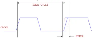
[image:1.595.349.532.678.755.2]As shown in Fig-1, jitter is the short-term variations of the significant instants of a digital signal from their ideal positions in time. The expected edges in a digital data stream never occur exactly where desired. Defining and measuring the timing accuracy of those edges (jitter) is critical to the performance of synchronous communication systems.
Fig. 1. Jitter in clock signals
Low Jitter Circuits in Digital System using
Phase Locked Loop
Ahmed Telba, Member, IAENG
Jitter is caused by several factors such as:
Power supply noise passing through a Phase Locked Loop (PLL) produces an output signal with a jitter.
The noise on the PLL’s reference frequency signal PLL in a frequency synthesizer has a dead-band associated with it, during which the phase and frequency detector does not detect small changes in the input phase. Since these changes are not detected, they do not get corrected and appear on the outputs in the form of jitter. Random and thermal noise from the crystal reference resonating device. Mechanical noise vibrations of the crystal reference.
Optical and electrical connectors for cables create switching noise. Cross-talk: as it produces phase variations in the transmitted digital signal. It arises from magnetic field generated by nearby signals.
Hence, the clock recovery PLL must be able to regenerate the time signal of the incoming data correctly and track any jitter at different frequency ranges so that no data is lost, this is called Jitter Tolerance (JT). The JT analysis of recovery circuit shows that the amount of incoming data jitters at low frequencies can be quite large. In addition, a very narrow band PLL may not be able to lock on to the incoming frequency since the capture range (the range of frequencies over which the PLL can make the oscillation frequency equal to the reference frequency) is a direct function of the bandwidth. These are the two key factors that determine the minimum bandwidth of the clock recovery circuit.
II.JITTER MEASUREMENTS
There are three famous kinds of jitter, namely cycle-cycle jitter, period jitter and long-term jitter. There are different methods for measuring them.
Measuring cycle-cycle jitter is extremely difficult. A timing interval analyzer (TIA) is required to perform this measurement. In this case, the output of the jittery clock is connected to a TIA, and the measurement to be specified is the difference of time periods of consecutive clock cycles. The maximum of this difference over multiple cycles is the cycle-cycle jitter. The cycle-cycle jitter can be measure by TIA, or by a high precision oscilloscope can be used to probe and sample the clock output, and a time interval measurement can be used to calculate jitter from the sampled data points. The time interval measurement can be used to calculate cycle-cycle jitter and peak-peak period jitter over a number of cycles. The maximum number of cycles over which this measurement can be taken is limited by the memory size of the oscilloscope. Measuring period jitter requires any wide band storage oscilloscope with some adjustments. Long-term jitter is probably the easiest to measure. It uses a measuring technique called differential phase measurement. The jittery clock is connected to an oscilloscope with a delayed time-base feature. The scope is set to trigger on the rising edge of clock. Then, using the delayed time-base feature, the same clock waveform is displayed on the screen.
To make sure that the scope calibration and characteristics can perform the jitter measurement, measure the output of a stable clock source, like a crystal oscillator. If the waveform has no blurs or bands, the scope can
correctly measure long-term jitter.
III.STATEMENT OF THE PROBLEM
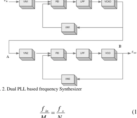
The block diagram of a dual PLL frequency Synthesizer is shown in Fig. 2. The circuit consists of two PLL connected in cascade i.e., the output generated by the first one is supplied as an input to the second PLL. The first one is a PLL which uses a Voltage Controlled Crystal Oscillator (VCXO) with a centre frequency of fx not necessarily equal to fin and the second one is a narrow band PLL with a wide sweep range [6, 7]. Bandwidths of the two PLL are carefully selected to minimize the overall output jitter.
The VCXO produces a low jitter output signal. A frequency divider producing a divide-by-N, allow the VCXO to operate at N multiples of the reference clock provided by an oscillator running at T1 carrier (1.544 MHz). The divider output signal is compared to that of the oscillator by a Phase Detector (PD). A digital-to-analogue converter (DAC) is used to convert the digital output of the PD into an analogue signal which is fed to the VCXO after being filtered by a Low Pass Filter (LPF).
[image:2.595.316.545.402.599.2]The analogue VCO output is passed through an Analogue-to-Digital Converter (ADC) before being passed to the PD through the divider. When the first loop in lock condition [6], the equation (1) shown the lock condition
Fig. 2. Dual PLL based frequency Synthesizer
1
1 N
f M
fin x (1)
Similarly, for the second loop in lock condition
2
2 M
f N fout x
(2)
Using (1) and (2), we get
)
(
2 1
2 1
M
M
N
N
f
f
out
in (3)A. Phase Detector (PD)
The heart of a PLL based frequency synthesizer is PD. The PD is a circuit that produces an output signal that is proportional to the phase difference between two input signals. The library model chosen for a PD is a simple Exclusive OR (EXOR) gate.
B. Loop filter
Loop filter is low pass filter (LPF) allows only the low frequency part of the phase difference to pass to the VCO. The high frequency part is filtered out. As a result, the PLL only tracks the low frequency variation and does not allow the high frequency variation.
LPF transfer function given in equation 4.
2 2
2
)
(
p p
w
s
Q
w
s
w
K
s
H
p
(4)where,
p
p
f
w
2
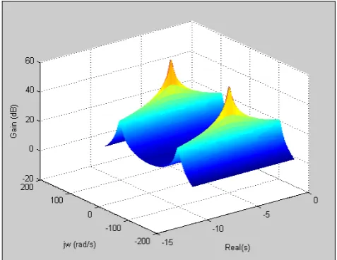
(5)The LPF is used for both PLLs but with different specifications. The first PLL uses
f
p= 5 KHz,K
= 1.0 andQ
[image:3.595.49.288.441.625.2]= 1.0, whereas the second PLL has the following design criteria:
f
p= 10 KHz,K
= 1.0 andQ
= 1.0, Fig .2 shows the loop filter response simulated in Matlab.Fig. 3. Loop filter response
Binary data generated by various systems must often be transmitted over long distances. For long distance serial data stream is usually used. Information is extracted from serial data streams by sampling the data signal at specific instants. Ideally these sampling instants would always occur at the center of a data bit time, equidistant between two adjacent edge transition points. The presence of jitter changes the edge positions with respect to the sampling point. An error will then occur when a data edge falls on the wrong side of
voltage-controlled oscillator (VCO) in terms of the statistical properties of supply noise and predicts the PLL timing jitter in response to the VCO phase noise. They design a low power, 2.5V, 0,25µ CMOS PLL clock generator with a lock range of 100MHz-400MHz, and use their mathematical model to study the jitter–induced P/G noise in this PLL. Yamaguchi, Soma, Ishida, Watanabe and Ohmi [13] classified jitter as either timing jitter or period jitter and discussed the two most popular (traditional) methods for measuring PLL jitter, namely: spectrum analyzer (phase detector method) for measuring phase noise and zero-crossing detector for measuring RMS and peak-to-peak period jitter[14-15]. Then they describe a new method for extracting both instantaneous and rms sinusoidal jitter from phase-locked loops (PLL) output signals. Their method is based on analytic signal theory and utilizes the Hilbert transform with a zero-crossing re-sampler to extract phase information from a PLL signal. With a low overall system noise and a sufficient over sampling ratio (by twice the nyquist rate), the method measures extremely small jitter in PLL signals optimally [16-17].
Fig. 4. Measured jitter using high speed oscilloscope
Zhang, Wang and Forbes [17], simulated the timing jitter in the first part of this paper due to CMOS device noise in a nine-stage CMOS differential ring oscillator and showed that the variation of absolute jitter due to flicker noise has t-dependence while for white noise it has 0.5–t-dependence.
In the second part of the paper, the authors investigate the timing jitter in silicon BJT and SiGe HBT ECL ring oscillators to show that they have lower jitter compared to their CMOS counterparts.
IV.EXPERIMENTAL RESULTS
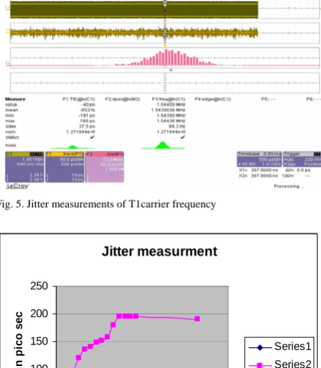
The dual loop system described above was built and tested using LeCroy oscilloscope "Wave Runner" model 6100 "1GHz sampling oscilloscope". The JTA2 software package for LeCroy oscilloscopes provides advanced jitter and timing analysis capabilities. It uses LeCroy’s long memory and zoom architecture to capture and precisely measure thousands of cycles of timing information and then present the results with three different views. By applying a high jittered signal to the system and measuring the output jitter at frequency 1.544 MHz (T1 Carrier) we can deduce the jitter behavior of the system .The output from the
[image:4.595.308.541.190.457.2] [image:4.595.46.288.322.470.2]oscilloscope is as shown in Fig.5, where the upper part shows the carrier frequency. The middle portion of the figure shows the Jitter track. The lower portion is the jitter histogram. The jitter statistics were taken mainly (cycle to cycle jitter, RMS jitter and accumulated jitter). The TIE has also been measured. It is clear from the figure that the value of the jitter was reduced dramatically from 5.6 nano seconds in input to 37.5 pico seconds in output. The test is repeated at different carrier frequencies and the output RMS is plotted versus the carrier frequency in Fig.7[19-20].
Fig. 5. Jitter measurements of T1carrier frequency
Jitter measurment
0 50 100 150 200 250
0 10 20 30
frequency in MHz
Ji
tt
er
i
n
p
ico
sec
Series1 Series2
Fig.6. Output Jitter at different carrier frequencies
V.CONCLUSION
Extensive research work has been done so far towards analyzing, modeling and overcoming the problem of jitter associated with clock recovery circuits. This helped to develop an improved de-jitter circuit that may add some features to the already existing VCXO technique which has been done by using two cascaded PLLs; the first one is low jitter using voltage controlled crystal oscillator and the second is a normal PLL .The first one uses a voltage controlled crystal oscillator (VCXO) with a center frequency not necessarily equal to the input frequency and the second is a PLL with wide sweep range.
[image:4.595.306.540.341.535.2]REFERENCES
[1] D.Wolaver, Phase-Locked Loop Circuit Design, Prentice Hall, 1991. [2] Floyed M.Gardner, Phaselock Techniques, Wiley; 2nd edition 1979. [3] Roland E. Best, Phase-Locked Loops: Design, Simulation, and
Applications,McGraw-Hill, NY 1999.
[4] DART Dejitter PLL Design and Analysis AN-531 application note DART Device TXC-02030-AN2 TranSwitch Corporation.
[5] Simulating Phase Noise in Phase-Locked Loops With a Circuit Simulator Thain, W.E.,Jr.;Connelly,J.A.;Circuits and Systems, 1995. ISCAS '95., 1995 IEEE International-Symposium-on, Volume:3, 28April-3May-1995-Pages:1760-1763 vol.3.
[6] Jitter in PLL-Based Systems: Causes, Effects and Solutions (Cypress Semiconductor Corporation 1997)
[7] A General Theory of Phase Noise in Electrical Oscillators Hajimiri, A.; Lee, T.H.;Solid-State Circuits, IEEE Journal of , Volume: 33 , Issue: 2 , Feb. 1998 Pages:179 - 194.
[8] A study of Oscillator Jitter Due to Supply and Substrate Noise Herzel, F.; Razavi, B.;Circuits and Systems II: Analog and Digital Signal Processing, IEEE Transactions on [see also Circuits and Systems II: Express Briefs, IEEE Transactions on] , Volume: 46 , Issue: 1 , Jan. 1999 Pages:56 - 62.
[9] A Novel Charge Pump PLL with Reduced Jitter Characteristics Myoung-Su Lee; Tae-Sik-Cheung;Woo-Young-Choi; VLSI and CAD, 1999. ICVC'99 6th International Conference-on-, 26-27Oct.1999 Pages:596 - 598.
[10] Jitter effects on Analog to Digital and Digital to Analog Converters (Troisi Design Limited, Application note 2000).
[11] Analysis of Jitter due to Power-Supply Noise in Phase-Locked Loops Heydari, P.; Pedram,M.;Custom Integrated Circuits Conference, 2000. CICC. Proceedings of the IEEE-2000-, 21-24-May2000-Pages: 443 - 446.
[12] Jitter-Induced Power/Ground Noise in CMOS PLLs: A Design Perspective Computer Design, Heydari, P.; Pedram, M.; 2001. ICCD 2001. Proceedings. 2001 International Conference on 23-26-Sept.2001 Pages: 209 - 213.
[13] Extraction of Instantaneous and RMS Sinusoidal Jitter Using an Analytic Signal Method (Yamaguchi, Soma, Ishida, Watanabe and Ohmi, 2002) IEEE Transactions On Circuits And Systems-Analogue And Digital Signal Processing, Vol. 50.NO 6 June 2003.
[14] Study and Simulation of CMOS LC Oscillator Phase Noise and Jitter (McCorquodale, Ding and Brown, 2003). Michael S. McCorquodale, Mei Kim Ding, and Richard B. Brown, Proceedings or the International Symposium on Circuits and Systems (ISCAS '03), Bangkok, Thailand, Vol. 1, pp. 665-668, May 25-28, 2003.
[15] Approximation Approach for Timing Jitter Characterization in Circuit Simulators Gourary,M.M.;Rusakov,S.G.;Ulyanov, S.L.; Zharov, M.M.; Gullapalli, K.K.; Mulvaney, B.J.; Design, Automation and Test in Europe Conference and Exhibition, 2003 , 2003 Pages:156 – 161. [16] T. Pialis and K. Phang, "Analysis of Timing Jitter in Ring Oscillators
Due to Power Supply Noise," IEEE International Symposium on Circuits and Systems, Bangkok, Thailand, Vol. 1, pp. 685-688, May 2003.
[17] Zhang, Wang and Forbes “Simulation technique for noise and timing jitter in electronic oscillators ”IEE Proc-circuits Devices and Syst.,Vol. 151,No.2 April 2004.
[18] M.Abou El Ela, J. M. Noras, and A. Telba “Desynchronizer Circuit in SDH System Using Digital PLL” “Proceedings of ICECS 2003 Conference IEEE Circuits and Systems Society, University of Sharjah, UAE.