Co-evolutionary Approach to Reduce Soft Error Rate of
Implemented Circuits on SRAM_based FPGA
Hadi Jahanirad
Department of electrical engineering, University of Kurdistan Pasdaran Street, Sanandaj, Iran
ABSTRACT
Soft errors such as Single Event Upset (SEU) have great effect on performance degradation of circuits implemented on SRAM_based FPGA. The soft error in configuration bits which control the logic and routing parts of the circuit, leads to permanent faults. In this paper, we have developed a co-evolutionary method to reduce the effect of soft error on the implemented circuit on FPGA. This method is based on cooperation of genetic algorithm and ant colony optimization. The efficiency of co-evolutionary method has been proved by comparison of its results with the proposed genetic algorithm and ant colony optimization. The experimental results for some MCNC benchmark circuits show up to 34% improvement compare to genetic algorithm and up to 60% improvement against ant colony optimization.
Keywords
Soft error rate, SRAM_based FPGA, Place and route, GA, ACO
1.
INTRODUCTION
The Field Programmable Gate Array (FPGA) has used in wide range of application such as aerospace. There are various types of this chip from various vendors. The conventional FPGA architecture consists of a two-dimensional (2-D) array of identical configurable Logic Blocks (LBs), surrounded by programmable Input/output Blocks (IOBs). The LB usually consists of a Lookup Table and a DFF. The LBs have been connected using a programmable interconnect network, which consists of switch matrices and wires. Almost 80% of transistors in an FPGA lay inside this programmable routing network (programmable switches and buffers). In modern FPGAs, more than fourteen layers of metal are used, most of them for routing resources [1].
Single Event Upset (SEU) is the most important source of soft error in aerospace applications. FPGAs are more vulnerable to SEUs compared to Application Specific Integrated Circuits (ASIC) [2]. In SRAM-based FPGAs, all programmable resources (particularly routing switches) are configured by SRAM cells; these devices are very susceptible to such errors [3]. The energetic particles such as neutrons from cosmic ray and alpha particles generating electron–hole pairs as they pass through a semiconductor device [4]. If the amount of accumulated charges collected at the drain of the off MOSFET in an SRAM cell is sufficient an inversion in the state of the SRAM cell may occur [4].
The effects of SEUs in an SRAM-based FPGA may lead to the following faults: (1) SEUs may alter the contents of SRAM cells used in the implemented circuit. For example, SEUs may alter the contents of DFFs used in the circuit or the control unit. (2) SEUs may alter the contents of the FPGA’s configuration memory, which defines the function of logic resources (e.g. lookup tables or LUTs) as well as their
interconnection (e.g. routing switches) [5]. Type 1 is transient because the faulty bit can be overwritten, while type 2 is permanent because the configuration bits remain unchanged until configuration bit stream re-downloaded into the FPGA [6].
Reliability is actually as important as other factors such as cost, performance, power consumption, area overhead and speed in the design of digital circuits [7], [8]. Reliability analysis of a logic circuit composed of logic gates, estimates the probability of a correct output value when the circuit is subject to an error stress such as incorrect input or internal gate failure. A common technique for reliability analysis of logic circuits is based on Monte Carlo framework which is based on fault injection into the nodes of the circuits and calculation of circuit output values by applying various input vectors [9]. The main problem of this method is its inapplicability to large circuit and large number of input vectors. References [10-14] have introduced analytical methods based on Discrete Time Markov Chains (DTMC) and Binary Decision Diagrams (BDDs). The reliability analysis based on signal probability can be found in references [15-19].
References [20] and [21] have proposed two algorithms for reliability analysis of combinational circuits. The first algorithm is called observability-based reliability analysis and the second is called single-pass reliability analysis. The concept of these algorithms is based on the fact that an error at the output of any gate is the cumulative consequent of a local error component related to that gate, and a propagated error component related to the failure of gates in its transitive fan-in cone. In [22] a reliability analysis for sequential circuits is presented based on second method.
In this paper we have presented a signal probability method for estimating soft error rate of FPGA implemented designs. In this method we have considered single fault occurrence in LUT cells and programmable routing switches. In addition, the problem of re-convergent fan-outs has been solved using 16 correlation coefficients approach which leads to accurate results.
to placement problem in FPGA in references [29-31]. All of this method define their fitness function based on bounding box which presents a weak estimation of the wirelength cost so we have introduced another fitness function based on Minimum Steiner Tree (MST) which not only has better estimation of wirelength but also as a goal in global routing estimates the congestion of wires in routing resources. Our proposed methods based on GA and ACO introduce new and more appropriate operators and adaptation approach.
This paper is organized as follows: Soft error rate estimation method has been described in section 2. In section 3 the fitness function has been introducedfor the proposed evolutionary methods. Adopted genetic algorithm and ant colony methods described in section 4 and 5 respectively. The co-evolutionary method to reduce soft error rate has been presented in section 6. Experimental results for some benchmark circuits presented in section 7 and conclusion has been drawn in section 8.
2.
Soft Error Rate Estimation
Soft errors such as SEU have great effect on FPGA memory elements in aerospace applications. There are two types of FPGA’s memory resources; first, user bits (DFFs) in which the SEU can alter the content of them directly or passing through a combinational path. This type of soft error is essentially transient and disappears after writing new data in the affected DFF. Configuration bits as the second type of memory resources, constitute more than 98% of all memory elements in the SRAM_based FPGA [32], [33]. The configuration bits configure routing switches and LUT cells as combinational logic part of implemented circuit. An SEU that upsets a configuration bit has a permanent effect until the original configuration bit-stream be re-downloaded into the FPGA.
Single fault in integrated circuits is the most probable fault type. A brief view at fault in time (FIT) and mean time to failure (MTTF) of SEU in SRAM_based FPGA from XILINX corporation declares that considering single fault model for faults leads to accurate results in soft error analysis (probability of multiple fault occurrence is negligible). Single fault can occur in the logic and routing parts of an implemented design and we model these faults as follows.
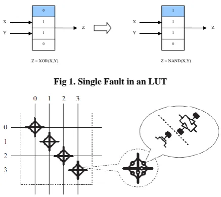
• LUT Single Fault Model: An LUT is an N×1 RAM (where N is a power of two, e.g. a 16×1 RAM) in which an arbitrary logic function of up to log2N inputs can be implemented. The contents of this N-cell RAM are determined through FPGA’s configuration operation. Single Event Upset (SEU) may change the contents of these cells temporarily or permanently (Fig. 1). Single fault occurrence in any of LUT cells may change the logic function implemented on it (e.g. in Fig. 1 the faulty cell changes the LUT function from XOR to NAND).
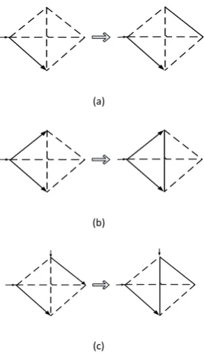
• Programmable Switch Single Fault Model: The routing resources (wire segments and bidirectional switches) occupy a large portion of the FPGA chip. Consequently, SEU induced faults have occurred in these parts more likely. The most vulnerable elements of routing resources are programmable switches, which are used to make connection between horizontal and vertical wire segments. A programmable switch can be either a buffer or a pass transistor (Fig. 2). Each programmable switch is controlled by six bits of configuration memory. A fault occurrence in these control bits may lead to a net getting misrouted or disconnected.
The programmable switches constitute switch boxes which make a flexible structure to routing affair. There are different
architectures for switch boxes in SRAM_based FPGA of various vendors. In this paper we have selected disjoint switch box architecture (Fig. 2). Disjoint switch boxes have been used in industrial FPGAs [34], in which a wire i of one box’s side can connect only to other wires i in the other three sides of switch box. If we want to connect any pairs of four wires in the four sides of switch box, we should use six programmable switches in their cross-point.
When a single fault occurred in a programmable switch, one of the following cases will arise:
• Zero to one transition in a control bit: in this case an unused switch of six switches will be on. This may have no effect on the system operation (Fig. 3-a), make a connection between two wire with same driver (Fig. 3-b) or make a connection between two wires with different drivers (Fig. 3-c). The last case leads to an unknown state in the output wires of the switch (‘X’ logic value).
• One to zero transition in a control bit: in this case a switch which is on turned off and causes a floating state (discontinuity in a path). This disconnection maybe interpreted as a logic ‘0’ or logic ‘1’ in the destination of the path, so in this case we assign “X” value to the output wire of the related switch.
The signal probability propagation is a common method in power analysis and signal activity computation. The reliability analysis of logic circuits using signal probability propagation method has been discussed in literature extensively. While in previous works only two logic levels of 0 and 1 have taken into account, in this work, we have considered three standard logic values of 0,1 and X beside an additional value of Y.
An FPGA implemented circuit seats on LBs (LUTs and DFFs) connected together by switch boxes (containing programmable switches) and wire segments. We describe our method to propagate weight values through these parts below.
0 1 1 0
1 1 1 0
Z = XOR(X,Y) Z = NAND(X,Y)
X
Y
Z
X
Y
[image:2.595.319.538.456.651.2]Z
Fig 1. Single Fault in an LUT
(a)
(b)
[image:3.595.101.248.68.322.2](c)
Fig 3. Zero to one transition in programmable switch
• Propagation weight through LUT: For each input of LUT there are four distinct weights: w0, w1, wx, wy (logic y is the invert of logic x). The output weights of this logic element can be computed using the weights of inputs and the its logic function. For example, the output weights of an XOR gate (with its inputs labeled a and b) can be computed according to Eq. 1-4. ) ( ) ( ) ( ) ( ) 1 ( ) 1 ( ) 0 ( ) 0 ( ) 0 ( Y w Y w X w X w w w w w w b a b a b a b a out (1) ) ( ) ( ) ( ) ( ) 0 ( ) 1 ( ) 1 ( ) 0 ( ) 1 ( X w Y w Y w X w w w w w w b a b a b a b a out
(2)
) 1 ( ) ( ) ( ) 1 ( ) 0 ( ) ( ) ( ) 0 ( ) ( b a b a b a b a out w Y w Y w w w X w X w w X w
(3)
) 1 ( ) ( ) ( ) 1 ( ) 0 ( ) ( ) ( ) 0 ( ) ( b a b a b a b a out w X w X w w w Y w Y w w Y w
(4)
In our method, the re-convergent fan-outs have been handled by defining correlation coefficients between a pair of fan-out branches (Cij) and propagating these coefficients to the re-convergence point. So for each LUT, the correlation coefficients considered in the derived formulas. For example, for “XOR” gate the modified formulas are as follows:
) ( ) ( ) ( ) ( ) ( ) ( ) 11 ( ) 1 ( ) 1 ( ) 00 ( ) 0 ( ) 0 ( ) 0 ( YY C Y w Y w XX C X w X w C w w C w w w ij j i ij j i ij j i ij j i out (5) ) ( ) ( ) ( ) ( ) ( ) ( ) 10 ( ) 0 ( ) 1 ( ) 01 ( ) 1 ( ) 0 ( ) 1 ( YX C X w Y w XY C Y w X w C w w C w w w ij j i ij j i ij j i ij j i out (6) ) 1 ( ) 1 ( ) ( ) 1 ( ) ( ) 1 ( ) 0 ( ) 0 ( ) ( ) 0 ( ) ( ) 0 ( ) ( Y C w Y w Y C Y w w X C w X w X C X w w X w ij j i ij j i ij j i ij j i out (7) ) 1 ( ) 1 ( ) ( ) 1 ( ) ( ) 1 ( ) 0 ( ) 0 ( ) ( ) 0 ( ) ( ) 0 ( ) ( X C w X w X C X w w Y C w Y w Y C Y w w Y w ij j i ij j i ij j i ij j i out
(8)
•Propagation Weights through Routing Switches: As mentioned before a path between an LUT or IO and another LUT contains some wire segments and programmable switches. If there is no fault in a path the weight values of the source of this path propagate to the destination of the path directly. Occurrence of single fault in the programmable switches of this path may cause a floating node in the path or a collision with other path (Fig. 3). These types of faults change the weight values of the destination as follows:
0 ) ( , 1 ) ( , 0 ) 1 ( , 0 ) 0
( w w X wY
w (9)
In the combinational circuit analysis, we divide the fault into two types: single fault in an LUT cell and single fault in a programmable switch.
Single fault in an LUT cell toggles the logic of that cell; so for each cell of the LUT we consider this change and compute w0, w1, wX and wY in the output of the circuit. The difference between these weights and the corresponding values of fault free circuit are used for error calculation:
LUT cells cntt Logic
Logic
i
Err
i
t
rr
E _ _ 1)
,
(
)
(
(10) Where:
)
(
)
(
)
(
)
(
)
,
(
i
t
w
0i
w
1i
w
i
w
i
rr
Logic X YE
(11) ) ( ) ( )
(i w _ i w i
w Fault Free Faulty
(12)
ErrLogic(i,t) is the error of primary output i caused by a toggle in cell t ,∆w0,1,X,Y(i) is the difference between weights of fault free and faulty states and ErrLogic(i) is the total error of output i caused by single fault occurrence in the logic part.
Single fault in programmable switches may cause the signals travelling from source LB to sink LB(s) to become faulty. The faulty value of switched signal is determined regarding its configuration as described in eq. 14. After modifying w0, w1, wX and wY in the inputs of sink LBs connected to faulty switch, we can propagate these values to the outputs of circuit and compute the new values of the outputs. Error caused by the faulty switch is calculated as:
control bits cntt
Routing
Routing
i
Err
i
t
rr
E _ _ 1)
,
(
)
(
(13) Where:
)
(
)
(
)
(
)
(
)
,
(
i
t
w
0i
w
1i
w
i
w
i
rr
Routing X YE
(14)
) ( )
( )
(i w _ i w i
w Fault Free Faulty
(15)
again ErrRouting(i,t) is the error of primary output i caused by a toggle in control bit t , ∆w0,1,X,Y(i)is the difference between weights of fault free and faulty states and ErrRouting(i) is the total error of output i caused by single fault occurrence in a programmable switch.
3.
FITNESS EVALUATION
circuit on FPGA decreases the number of fault sites will be decreased and the error rate will be decreased accordingly. Because of existence of very good synthesis tools we do not develop such tool but we use the “netlist” which generated by these tools, to develop more reliable place and route method.
The second factor which is very effective in reduction of the error rate is the approach which is applied to place the LUTs of the “netlist” on the FPGA and selection of the programmable switches and wire segments used in the routing process of such “netlist”. The main idea to reduce the soft error rate in this paper is optimizing the place and rout in such a way that the number of used programmable switches (most vulnerable elements to soft error) reduced as well as the congestion of switches and risky configuration of the switches be avoided.
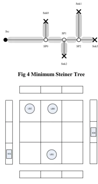
As mentioned before the routing between each node and its sinks will be done using wire segments and programmable switches. Once the nodes (LUTs) placed on the specific cells of FPGA we should construct the necessary routs in way that the minimum length will be met and the congestion be avoided. These routes are constructed using minimum Steiner Tree (MST) for the node and its sinks. The MST for node ni has been shown in Fig. 4.
To derive a straight-forward expression for the fitness function, we have defined two terms; first one is the placement cost which is the sum of MSTs’ length of all implemented circuit’s nets (eq. 16). Second term is related to congestion of routes in the implemented circuit. We have defined a congestion weight for each programmable switch and for each switch used in the MST of the node we increase this weight. After routing process, more uniformly distributed switch weights can be interpreted as less congestion and more reliable implementation. So for second term in the fitness function we have used the standard deviation as the congestion cost (eq. 18). In this equation NSW is the total number of switches used in the circuit implementation. is the mean of weights of used switches and wi is the weight of switch number i. after calculation of place_cost and congest_cost we can derive fitness of the placed and routed circuit using eq. 19.
4.
GA-BASED APPROACH FOR SOFT
ERROR RATE REDUCTION
In this section we first introduce our approach to build genetic system which is compatible with our problem and then overall procedure for optimizing the fitness function will be introduced.
• Chromosome structure: in each generation of genetic algorithm, there are N individuals each of them called a chromosome. Each chromosome can be assumed as a solution for the problem which consists of some genes. Each gene describes a part of the complete solution. In our problem we define each chromosome as a distinct placement of the netlist on the FPGA. So each gene of the chromosome will be the position of an LB or IO of the netlist.
(17)
(18)
(19)
Src
Snk0
Snk1
Snk2
Snk3 SP0
SP1
[image:4.595.344.505.71.371.2]SP2
Fig 4 Minimum Steiner Tree
LB2 LB0
LB1
IO0
IO1
Fig 5 Placement of a circuit with 2 IO and 3 LB
Common architecture of FPGA is a 2 dimensional array of LBs which surrounded by IO blocks, so for each gene there is two numbers: first number is the row index of corresponding block and the second one is its column index. As an example assume the netlist has three LBs and two IOs, one possible placement of the netlist on a 3×3 FPGA has been indicated in Fig. 5. The corresponding chromosome is as follows:
Chromn = [(3,0),(2,4),(1,2),(3,2),(1,1)]
The first element of ith pair is the row index of gene i and the second one is the column index of the gene. The first two genes correspond to IOs and the last three genes correspond to LBs.
• Genetic Operators: The key concept in the genetic algorithm is directed scanning of a big search space to find optimum results. This can be done by applying genetic operators to one generation of chromosomes in a mating pool and construct next generation using natural selection. To build a mating pool in the generation n, all chromosomes would be evaluated based on fitness function and then based on its score the number of each chromosome which go to mating pool is determined. Genetic operators will be applied to the chromosomes in the mating pool as follows.
Chroma = [(0,1),(3,0),(3,2),(1,1),(2,5),(4,3),(5,5)]
Chromb = [(6,3),(0,4),(2,5),(3,1),(5,3),(4,4),(5,1)]
Chromchild1 = [(0,1),(3,0),(3,2),(3,1),(5,3),(4,4),(5,1)]
Chromchild2 = [(6,3),(0,4),(2,5),(1,1),(2,5),(4,3),(5,5)]
In our proposed crossover operator, the above problem has been handled as follows. First of all, proposed crossover is based on single parent and lead to single child. The parent chromosome divide into IO and LB parts then for each part the number of genes which must be swapped is determined (pIO,pLB). In LB (IO) part pLB/2 (pIO/2) pair of genes has been selected randomly, then the position of genes in each pair swapped. The produced child has an acceptable similarity to its parent, moreover there is no problem such as gene replica in its structure.
Mutation: The conventional mutation operator is done by changing some genes of a chromosome randomly and produces a new chromosome. This operator extends the scope of the algorithm search and resolves trapping in local minima. Applying this operator for our problem may lead to unacceptable child. For example, in the following chromosome if we mutate fourth gene (LB position) on chromosome randomly the resulted child may have a replication (Chromchild1) or an IO position selected for that LB (Chromchild2).
Chromb = [(6,3),(0,4),(2,5),(3,1),(5,3),(4,4),(5,1)]
Chromchild1 = [(6,3),(0,4),(2,5),(5,1),(5,3),(4,4),(5,1)]
Chromchild2 = [(6,3),(0,4),(2,5),(3,6),(5,3),(4,4),(5,1)]
We modify this operator as follows: the chromosome is divided into IO and LB parts which will be mutated separately. For each part we determine the number of genes which must be mutated (pm,IO,pm,LB), then we select randomly pm,LB(pm,IO) genes from LB(IO) part randomly. The position of selected genes will be substituted with an unused position of FPGA. Since the substituted positions are not used in the parent genes this modified version of mutation does not suffer from gene replica, in addition the scope of search would be extended by using unused positions.
5.
ACO-BASED APPROACH FOR SOFT
ERROR RATE REDUCTION
Traveler Salesman Problem (TSP) is a conventional problem in computer science. The bench of this problem constitutes a connected graph in which some cities (nodes) are connected by weighted edges. Each solution for TSP is finding a tour which visits each node of graph one time and all nodes have been visited. In this section we first introduce TSP model of our problem then the optimization method will be described.
To construct the graph, we have defined a node for each IO or LB. Starting from first node we must assign it to a position on FPGA and then go to the next node. If the node is an IO (LB) we can assign it to one of the unused IO (LB) positions. This process will be terminated when the last node assigned to a specific position.
The main concern in this algorithm is the selection of the position for the node from the unused positions. ACO do this based on a probability approach. When ant k in its tour wants
to assigns a position to node i there will be Nik possible positions. The probability of selection position j would be derived from eq. 20.
(20)
In which aij could be calculated using eq. 21.
(21)
In this equation ηij is a heuristic value for assigning position j to node i. we have determined this value for node i using the position of preceding nodes. For this goal we calculate partial cost of the node (place_cost and congest_cost) using placed nodes till now and use the inverse of it as ηij. The parameter τij is the tendency of ants to select position j for node i in pervious algorithm iterations. This parameter called pheromone trail of the specified edge.
(22)
After all ants in one generation complete their tours, each ant deposits following pheromone trail on the edges which has been visited by it.
In this equation fitnessk is the cost value of the ant k and Tk is the set of all edges have been visited by it. The pheromone changing of each edge j will be calculated using eq. 23 in which m is the total number of ants.
(23)
(24)
Finally, the pheromone trail will be updated using eq. 24 for the next generation use. In this equation ρ is the pheromone decay coefficient.
6.
CO-EVOLUTIONARY APPROACH
FOR SOFT ERROR RATE REDUCTION
Precocity and Stagnation are two major problems in conventional evolutionary algorithm such as ACO and GA. These two phenomena arise when the convergence rate of algorithm becomes slow. To measure these phenomena, we have defined two criteria in ACO and GA. First of which is a convergence criterion which has been defined using eq. 25.
(25)
In this equation we use gradient of mean cost of successive generations as the convergence definition. L is the number of previous generations which convergence judged upon them. The gradient between generation i and i-1will be computed using eq. 26. When the gradient value decreases the algorithm tends to converge which maybe resulted in precocity or stagnation.
(26)
(28)
The second criterion is diversity which defined in eq. 27. In each generation of algorithm for node n (LB and IO) of the netlist the number of different position which have been used by all individuals (ants or chromosomes) is defined as dpn parameter. When this parameter becomes small the diversity will become smaller.This means that algorithm has centralized on some region of search space which may lead to local minima trapping.
The flowchart of coevolutionary optimization has been indicated in Fig. 6. In the first step m solution for our problem generated randomly. Then one of the evolutionary method introduced in previous sections started using the primary generation (in this paper we first use ACO as our initial algorithm). After completing an iteration of algorithm the convergence and diversity criteria would be computed for current generation. The decision making function which defined in eq. 28 has be evaluated then based on its value the current algorithm (1) or the other one (0) is selected for next iteration. In this equation μ1 and μ2 is adjustable parameter to determine the importance of convergence and diversity in the decision and α is the parameter which determines the border of decision. This parameter is different for various circuits.
[image:6.595.311.548.63.573.2]The solutions which are produced in iteration by one of the algorithm will be stored in an optimum register and used as the current generation in the next iteration. After storing optimum register, the stopping criteria of algorithm have been tested and the stop or continue state will be selected upon it.
Fig. 6 Flowchart of Co-Evolutionary algorithm
[image:6.595.316.547.83.309.2]Fig. 7 Architecture of an LB
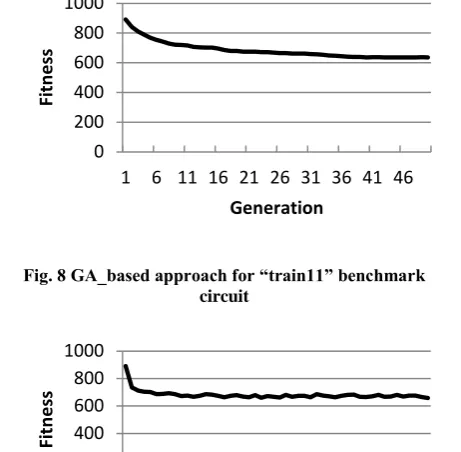
Fig. 8 GA_based approach for “train11” benchmark circuit
Fig. 9 ACO_based approach for “train11” benchmark circuit
Fig. 10 Comparison three approach for “train11” benchmark circuit
7.
Experimental Results
The FPGA architecture which has been used in this paper contains simple LBs (one 4 input LUT and a DFF as shown in Fig. 7). The LBs surrounded by IO blocks and the routing network is the main parts of the architecture. The routing network contains wire segments and switch boxes. Wire segment connects adjacent switch boxes (there are N tracks between two horizontal or vertical switch boxes). As mentioned before we use disjoint architecture for a switch box.
As an experimental result we apply our optimization method to some MCNC benchmark circuits. The MCNC benchmark circuits describe in “blif” file format in which the input, LB and output connection and the logic behavior of each LUT are presented. We use this file as “netlist” of the circuit. In the first experiment the reduction of soft error rate investigated
0 200 400 600 800 1000
1 6 11 16 21 26 31 36 41 46
Fi
tn
e
ss
Generation
0 200 400 600 800 1000
1 6 11 16 21 26 31 36 41 46
Fi
tn
e
ss
Generation
0 200 400 600 800 1000
1 6 11 16 21 26 31 36 41 46
GA ACO Coevolution
Generate m valid individual randomly
Do ACO for one iteration
Do GA for one iteration
Update optimum population Evaluate Decision
Making Function
Stopping criteria met?
Finish Next algorithm is
ACO?
YES YES
[image:6.595.65.273.431.616.2]based on our proposed genetic algorithm method. In Fig. 8 the average cost of each generation has been shown for train11 benchmark circuit. This cost reduced gradually until algorithm reaches convergence at 50th generation. In table 1 the average costs of initial and last generation (which algorithm converged at it) have been indicated for the MCNC benchmark circuits. In the second experiment the reduction of soft error rate has been investigated based on our proposed ACO method. In Fig. 9 the average cost of algorithm iteration has been shown. This cost reduced gradually until algorithm reaches convergence. In table 1 the average costs of initial and last algorithm iteration (which algorithm converged at it) have been indicated for the MCNC benchmark circuits.
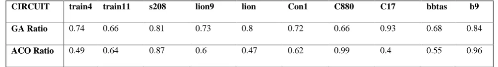
In the third experiment we have used our proposed co-evolutionary algorithm to reduce soft error rate. In Fig. 10 the average cost of iterations of algorithm has been compared to the previous results of GA and ACO based methods. It is seen that the cost of co-evolutionary method is far lower than the previous methods. In table 1 the average costs of initial and last algorithm iteration (which algorithm converged at it) have been indicated for the MCNC benchmark circuits. In table 2 we indicated the ratio of the mean cost of last generation for some MCNC benchmark circuits. In the second row this ratio calculated for co-evolutionary against GA_based method and
in the third row this ratio calculated for co-evolutionary against ACO_based method. The ratio for GA_based method starts from 0.66 in C880 and train11 to 0.93 in C17. So for all tested circuits the cost of co-evolutionary method is less than the cost of GA_based method so the error rate of co-evolutionary method is less than GA_based one. The ratio for ACO_based method starts from 0.4 in C17 and train11 to 0.99 in C880. So for all tested circuits the cost of co-evolutionary method is less than the cost of ACO_based method so the error rate of co-evolutionary method is less than GA_based one.
8.
CONCLUSION
[image:7.595.55.552.347.462.2]In this paper we develop three evolutionary methods to reduce soft error rate of implemented circuits on FPGA. First two methods are the adopted version of genetic algorithm and ant colony optimization and the third one is a co-evolution between these two methods. Applying these methods for implementing some MCNC benchmark circuits show that the cost of co-evolutionary method is smaller than the cost of the first two methods, so we can reach further reduction in soft error rate using the co-evolutionary approach. The experimental results for some MCNC benchmark circuits show up to 34% improvement compare to genetic algorithm and up to 60%.
Table 1. Mean Cost of Initial and Last Generation for Three Methods
CIRCUIT train4 train11 s208 lion9 lion Con1 C880 C17 bbtas b9
initCost 379.63 891.41 5757 680.48 346.45 644.75 40912 170.58 718.85 10920
GA Cost 176.82 636.22 5036.9 415.77 156.78 374.01 38250 63.46 461.56 9517.40
ACO Cost 264.20 657.47 4735.77 505.27 266.85 437.59 25500.32 148.16 571.90 8338.45
CoEvl Cost 130.39 420.50 4106.40 301.8 126.29 271 25306 59.18 314.32 8050.30
Table 2. Ratio of Mean Cost of GA_based and ACO_based to Co_Evolutionary Method
CIRCUIT train4 train11 s208 lion9 lion Con1 C880 C17 bbtas b9
GA Ratio 0.74 0.66 0.81 0.73 0.8 0.72 0.66 0.93 0.68 0.84
ACO Ratio 0.49 0.64 0.87 0.6 0.47 0.62 0.99 0.4 0.55 0.96
9.
REFERENCES
[1] J. Hogan, R. Weber and B. LaMeres, “Reliability Analysis of Field-Programmable Gate-Array-Based Space Computer Architectures,” J. Aerospace info. Syst., 2017, pp. 121–133.
[2] A. Sari, G. Agiakatsikas andM. Psarakis, “A soft error vulnerability analysis framework for Xilinx FPGAs,” in Proc. ACM/SIGDA int.symp. on Field-programmable gate arrays, 2014, pp. 234–240.
[3] P. McNelles, L. Lu, “Field Programmable Gate Array Reliability Analysis Using the Dynamic Flowgraph Methodology,” Nuclear Engineering and Technology, vol. 48, no. 5, Oct. 2016, pp. 1192-1205.
[4] K. A. Hoque, O. A. Mohammad, and Y. Savaria, “Formal analysis of SEU mitigation for early dependability and performability analysis of
FPGA-based space applications,” Journal of Applied Logic, vol. 25, no. 1, Dec. 2017, pp. 47–68.
[5] H.Ebrahimi, M. Saheb-Zamani, H.R. Zarandi, "Mitigating soft errors in SRAM-based FPGAs by decoding configuration bits in switch boxes", Microelectronics Journal, vol. 42, no. 1, January, 2011, pp. 12-20.
[6] H. Asadi, M.B. Tahoori, B. Mullins, D. Kaeli, K. Granlund, “Soft error susceptibility analysis of SRAM-based FPGAs in high-performance information systems”, IEEE Transaction on Nuclear Science, vol. 54, no. 6, 2007, pp 2714–2726.
[image:7.595.48.552.493.561.2][8] S. Bodapati, and K. Sridharan, “A transistor-level probabilisticapproach for reliability analysis of arithmetic circuits withapplication to emerging technologies,” IEEE Trans Reliability, vol. 66, no. 2, June 2017.
[9] C. Chen, and R Xiao, “A fast model for analysis and improvementof gate-level circuit reliability,” Integration, the VLSI Jour. vol. 50, pp. 107-115, Jun. 2015.
[10]Bhaduri D, Shukla S. NANOPRISM: “a tool for evaluating granularity versus reliability trade-offs in nano architectures”, Proceedings of the 14th ACM Great Lakes symposium on VLSI, 2004. p. 109–12.
[11]Norman G, Parker D, Kwiatkowska M, Shukla S. “Evaluating the reliability of NAND multiplexing with PRISM”. IEEE Trans Comput Aided DesIntegr Circuits Syst, vol 24, no. 10, pp1629–37, 2005
[12]Clarke E, Fujita M, McGeer P, Yang J, Zhao X, “Multiterminal binary decision diagrams: an efficient data structure for matrix representation”. Presented at the international workshop on logic synthesis (IWLS), Tahoe City, CA; 23–26, May, 1993.
[13]Akers SB. “Binary decision diagrams”. IEEE Trans Comput, 1978.
[14]Patel K, Markov IL, Hayes JP. “Evaluating circuit reliability under probabilistic gate-fault models”. Proceedings of the international workshop on logic synthesis (IWLS), 2003. pp. 59–64.
[15]Krishnaswamy S, Viamontes GF, Markov IL, Hayes JP. “Accurate reliability evaluation and enhancement via probabilistic transfer matrix”, Proceedings of the design, automation and test in Europe conference, 2005. [16]Franco DT, Vasconcelos MC, Naviner L, Naviner JF.
“Reliability analysis of logic circuits based on signal probability”, 15th IEEE international conference on electronics, circuits and systems, 2008.
[17]Franco DT, Vasconcelos MC, Naviner L, Naviner JF. “Reliability of logic circuits under multiple simultaneous faults”, 51st Midwest symposium on circuits and systems, 2008.
[18]Levin VL. “Probability analysis of combination systems and their reliability”. EngCybernet1964, pp 893–901.
[19]J. TorrasFlaquer, J.M. Daveau, L. Naviner , P. Roche. “Fast reliability analysis of combinatorial logic circuits using conditional probabilities”, Microelectronics Reliability, vol. 50, no.2, pp. 1215–1218, 2010.
[20]Choudhury MR, Mohanram K. “Accurate and scalable reliability analysis of logic circuits”. Proceedings of design automation and test in Europe (DATE), 2007. pp. 1454–9.
[21] Choudhury MR, Mohanram K. “Reliability analysis of logic circuits”. IEEE Trans Comput Aided Des Integr Circuits Syst, vol. 28, no. 3, 2009.
[22] S.J. SeyyedMahdavi , K. Mohammadi. “SCRAP: Sequential circuits reliability analysis program”, Microelectronics Reliability, vol. 49, no. 3, pp. 924–933, 2009.
[23] Marquardt A, Betz V, Rose J. “Timing-driven placement for FPGAs”. FPGA 2000: 203-213
[24] Betz V, Rose J. “VPR: A new packing, placement and routing tool for FPGA research. FPL 1997: 213-222
[25] Baruch, Z., Cret, O., Giurgiu, H., "Genetic Algorithm for FPGA Placement", in Proceedings of the 12th International Conference on Control Systems and Computer Science (CSCS-12), 1999, vol. 2, pp. 121-126. [26] Solar M, Perez J, Pulido J, Rodriguez M. “Placement and
Routing of Boolean Functions in Constrained FPGAs using a Distributed Genetic Algorithm and Local Search”. Parallel and Distributed Processing Symposium, April 2006
[27] Wang K, Ning X. “Ant colony optimization for Symmetrical FPGA Placement”. Computer-Aided Design and Computer Graphics, 2009. CAD/Graphics '09. 11th IEEE International Conference on, Aug. 2009, pp. 561 - 563
[28] Wenyao X, Kijun X, Xinmin X. “A novel Placement Algorithm for Symmetrical FPGA”. ASICON 7th International Conference on, Oct. 2007, pp. 1281 – 1284.
[29] Venayagamoorhy GK, Gudise VG. “Swarm Intelligence for Digital Circuit Implementation on Field Programmable Gate Arrays Platforms”. Evolvable Hardware, Proceedings. NASA/DoD Conference on, June 2004, pp. 83 - 86
[30] Gudise VG, Venayagamoorhy GK. “FPGA Placement and Routing Using Particle Swarm Optimization”. VLSI, Proceedings. IEEE Computer society Annual Symposium on , Feb. 2004, pp. 307 - 308
[31] El-Abd M, Hassan H,Kamel MS. “Discrete and Continuous Particle Swarm Optimization for FPGA Placement”. Evolutionary Computation, IEEE Congress on , May 2009 , pp. 706 – 711.
[32] Xilinx Corporation, San Jose, CA, “Virtex 2.5 V field programmable gate arrays,” Data Sheet DS003-1, 2001.
[33] H. Asadi, M.B. Tahoori, "Analytical techniques for soft error rate modeling and mitigation of FPGA-based designs," IEEE Transactions on Very Large Scale Integration (VLSI) Systems, Vol. 15, no. 12, December 2007.