Abstract―In this paper, a new approach for designing and implementing lifting-based VLSI architectures for two-dimensional discrete wavelet transform (2-D DWT) is introduced. As a result, two high performance VLSI architectures that perform 2-D DWT for lossless 5/3 and lossy 9/7 filters are proposed. In addition, the architectures implement symmetric extension for boundary treatment. First, two pipelined architectures consisting of two stages, the row and column processors stages, were developed for 5/3 and 9/7 filters. The internal memory between the row and the column processors is reduced to a few registers. Second, in order to speedup the computation, fully pipelined datapath architectures for row and column processors were separately developed for each 5/3 and 9/7 filters that can be incorporated into the two architectures developed in the first part. Finally, 100% hardware utilization is achieved.
Index Terms―VLSI architecture, discrete wavelets transform (DWT), JPEG2000, lifting scheme, and scan methods.
I. INTRODUCTION
The two-dimensional discrete wavelet transform (2-D DWT) has been applied as an effective and powerful tool in many
applications including image processing and compression [8], [9]. The 2-D DWT considered in this paper is part of a compression system based on wavelet such as JPEG2000. The function of the forward discrete wavelet transform (FDWT) in a compression system is to decorrelate the image pixels prior to the compression step [7]. Since the original image pixels are highly correlated, then directly applying compression algorithm to the original image pixels will not yield an efficient compression ratio. Thus, the power of DWT is to decorrelate the image pixels for effective compression. After transmitting to a remote site, the original image must be reconstructed from the decorrelated image. The tasks for reconstructing and completely recovering the original image are performed by the inverse discrete wavelet transform (IDWT).
The amount of data needs to be processed in both decorrelation and reconstruction steps is enormous that it requires very high processing power that can not be achieved by general-purpose processors, especially when real-time processing is required. Therefore, high speed and low power hardware for 2-D DWT is needed.
In this paper, two efficient and high performance VLSI
The authors are with the Electrical and Electronic Engineering Department, Universiti Teknologi PETRONAS, Perak, Tronoh, Malaysia (email: [email protected]).
architectures for 2-D DWT for 5/3 and 9/7 are presented. The two architectures are based on lifting scheme, which facilitates high speed and efficient implementation of wavelet transforms [1], [2]. Beside, it is also attractive for both high throughput and low-power applications. Therefore, the lifting-based DWT becomes the preferred scheme for VLSI implementation, and it has been selected as the transform coder for image compression in the released JPEG2000 standard. In addition, symmetric extension algorithm recommended by JPEG2000 for boundary treatment is incorporated and implemented by the two architectures.
This paper is organized as follows. In section II, the lossless 5/3 and lossy 9/7 algorithms are stated, and the data dependency graphs (DDGs) for both algorithms are established. Section III illustrates the overlapped and nonoverlapped scan methods. The two proposed architectures are presented in section IV. The performance evaluations and comparisons are discussed in sections V and VI, respectively. Conclusions are given in section VII.
II. LIFTING-BASED 5/3 AND 9/7 ALGORITHMS
The lossless 5/3 and lossy 9/7 wavelet transforms algorithms are defined by the JPEG2000 image compression standard as follow [5], [6]:
5/3 analysis algorithm
− + + + + = + + − + = + 4 2 ) 1 2 ( ) 1 2 ( ) 2 ( ) 2 ( : 2 2 ) 2 2 ( ) 2 ( ) 1 2 ( ) 1 2 ( : 1 j Y j Y j X j Y step j X j X j X j Y
step (1)
9/7 analysis algorithm
(
)
(
)
(
( )
(
)
)
( )
( )
(
(
)
(
)
)
(
)
(
)
(
( )
(
)
)
( )
( )
(
(
)
(
)
)
(
)
) 2 ( ) 2 ( : 6 1 2 1 ) 1 2 ( : 5 1 2 1 2 2 2 : 4 2 2 2 1 2 1 2 : 3 1 2 1 2 2 2 : 2 2 2 2 1 2 1 2 : 1 n Y k n Y step n Y k n Y step n Y n Y n Y n Y step n Y n Y n Y n Y step n Y n Y n X n Y step n X n X n X n Y step ′ = + ′ = + + ′ + − ′ + ′′ = ′ + ′′ + ′′ + + ′′ = + ′ + ′′ + − ′′ + = ′′ + + + + = + ′′ δ γ β α (2)The DDGs for 5/3 and 9/7 derived from the algorithms are shown in Figs 1 and 2, respectively. These graphs are very useful tools in providing guidance for architecture development and enhancement. The symmetric extension algorithm is incorporated into the DDGs to handle the boundary problems. The boundary treatment is necessary to keep the number of wavelets coefficients the same as that of the original. As shown in Figs 1 and 2, the boundary treatment is only applied at the beginning and the ending of the process [7]. That means in the 2-D images, it will be applied at the
beginning and the ending of each row or column.
Lifting-based VLSI Architectures for Two-
Dimensional Discrete Wavelet Transform for
Effective Image Compression
III. OVERLAPPED AND NONOVERLAPPED SCANNING METHODS
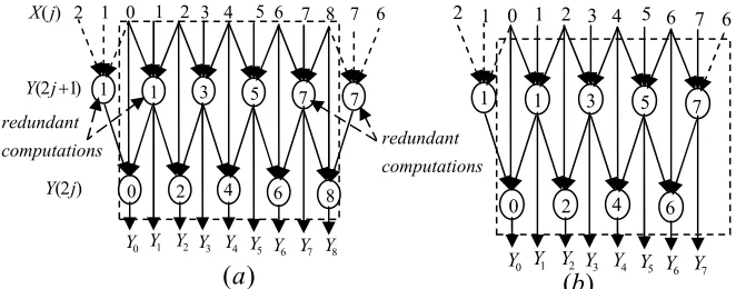
We believe that minimization of the internal memory, and hence the hardware complexity in general for 2-D DWT architectures, depends on the proper scan method adopted for scanning the external frame memory. Therefore, two scan methods, overlapped and nonoverlapped, are illustrated in Fig. 3(a) and (b), respectively. The pixels in the overlapped areas, indicated by the dark lines in Fig. 3a, are scanned twice. For an
N
×
M
image, this scan method requires
(
−1 2)
+ N M
NM clock cycles to scan the whole
image, whereas in the nonoverlapped method, the overlapped areas are eliminated to reduce the external memory access cycles to NM clock cycles only. The external memory access usually consumes the most power [4].
To ease the development of the architectures, the strategy adopted is to divide the details of the development into two steps each having small information to handle. In the first step, the DDGs are looked at from outside, which is specified by the dotted boxes, in terms of input and output requirements. We have observed that the DDGs for 5/3 and 9/7 are identical when they are looked at from outside, taking into consideration only the input and output requirements; but
differ in the internal details. Based on this observation, the first level of the architecture, call it, the external architecture, is developed. In the second step, the internal details of the DDGs are considered for the development of the processor’s datapath architectures, since DDGs internally define and specify the structure of the processors.
IV. PROPOSED ARCHITECTURES
A. External Architectures Development
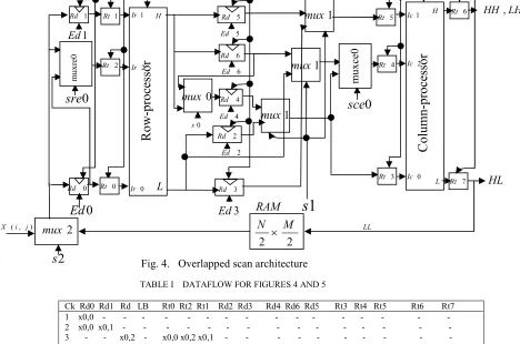
Based on the two scan methods shown in Fig. 3, and the DDGs for 5/3 and 9/7 when they are looked at from outside, the architectures shown in Figs 4 and 5 are proposed for overlapped and nonoverlapped scan methods, respectively. The architectures operate in a pipeline fashion, consisting of two stages, row-processor (RP) stage and column-processor (CP) stage. The two architectures are basically identical. The main difference is that the nonoverlapped architecture contains a line buffer (LB) of size N. In order to reduce the external memory access and hence the power consumption, the LB is added to hold N pixels that lay in each overlapped areas in Fig. 3(a). Pixels in an overlapped area such as column 2 are also required in the next N operations. According to the DDGs, each operation that performed by either RP or CP would require three inputs. For example, the input labeled 0,
1 2 5
3 1 1 3 5 7 5
2 0 2 4 6 6
1 1 3 5 7
0 2 4 6
1
Y
0
Y Y2 Y3 Y4 Y5 Y6 Y7
k k−1 k k−1 k k−1 k k−1
0 1
1 2 3
2
3 4
4 5 6 7 6 5 4
3 1 1 3 5 7 7 5
2 0 2 4 6 8 6
1 1 3 5 7 7
0 2 4 6 8
1
Y
0
Y Y2Y3Y4Y5Y6Y7Y8
k k−1k k−1k k−1k k−1k
) (n X
(2 +1)
′′ n
Y
( )n Y′′2
(2 +1)
′ n
Y
( )n Y′2
(2 1)
, ) 2 (n Y n+ Y
0 1
1 2 3
2
3 4
4 5 6 7 8 7 6 5 4
)
(
a
(
b
)
Fig. 1. 5/3 algorithm’s DDGs for (a) odd and (b) even length signals
Fig. 2. 9/7 algorithm’s DDG for odd (a) and even (b) length signals
0
Y Y1 Y2 Y3 Y4 Y5 Y6 Y7 1
1 3 5 7
7
0 0 2
2 1
1 2
4 4
3 5 6
6 6
0
Y Y1 Y2Y3 Y4 Y5 Y6 Y7 Y8
1
1 3 5 7 7
7 7
0 0
2 1
4 4
3 6
6
8 6
8 )
1 2 ( j+ Y
) 2 ( j Y
ns computatio redundant
) (j X
ns computatio redundant
)
(
a
(
b
)
[image:2.612.128.459.48.178.2] [image:2.612.112.491.218.413.2]1, and 2 in Fig.1 initiate the first operation to yield the coefficients labeled Y0 and Y1, whereas inputs 2, 3, and 4 initiate the second operation which yields Y2 and Y3 and so on. Fig.5 shows the nonoverlapped architecture from the RP side only, since its remaining parts are the same as in Fig.4.
Fig.3. Overlapped (a) and nonoverlapped (b) scan methods
In the following, the dataflow for the two architectures will be described. In the first clock cycle, the external memory’s location X(0,0) is read and is placed in register Rd0, as shown in table I. The second clock cycle reads location X(0,1) and places its contents in register Rd1 by the pulse ending the cycle. In the third clock cycle, location X(0,2) is read and is placed in the path leading to muxreo. Then by the pulse ending the cycle, contents of registers Rd1 and Rd0 including contents of location X(0,2) are transferred to the row-processor’s latches Rt1, Rt0, and Rt2, respectively. Another event also occurs during the third cycle in the nonoverlapped architecture, which is the transfer of location X(0,2) to Rd. Then, in the next cycle Rd is stored in the first location of the memory labeled LB, since it is needed in the next computation. While, in the overlapped architecture, location X (0, 2) is scanned again from the external memory. Now having the pipeline registers Rt2, Rt1, and Rt2 loaded with the required data, the RP can immediately be started to compute its first computation by the pulse ending the third cycle, which is also the beginning of the fourth cycle. This computation will last for three clock cycles, from cycle 4 to cycle 6, as indicted in Table I. The pulse ending cycle 6 transfers the results of the first operation, i.e., the first outputs of the RP, H(0,0) and L(0,0), to registers Rd4 and Rd2, respectively. In the fourth cycle, the scan moves to the second row of the external memory and repeats the process, as shown in Table I. The scanning process proceeds until it reaches the last row of the image, to complete, say, the first run. Then, returns to the first row to start the second run. This process is repeated until the whole pixels of an image are scanned, according to the scan method shown in Fig. 3.
Looking at the DDGs from outside, it can be observed that in the last high and low coefficients calculations, where the
row length of an image is even, only the last two pixels in a row, r, at locations X(r, M-2) and X(r, M-1) are read from external memory. In addition, the DDGs for even length, implementing the extension part, require the pixel located at X(r, M-2) to be considered as the first and the third inputs. And it must be passed to the RP with the second input pixel from location X(r, M-1), to compute the last high and low coefficients in row r. Thus, the function of the multiplexer labeled muxre0 is to pass pixel of location X(r, M-2), after it has been transferred to register Rd0, to the row-processor’s latch, Rt2, as the third input. Register Rd1 holds the second input, the pixel of location X(r, M-1). Similarly, the multiplexer labeled muxce0 performs the same function, when the column-processor applies DWT to columns. In other words, muxre0 and muxce0, which are extension multiplexers, are used only in the calculation of the last coefficient in even row or even column images.
On the other hand, when the row length of an image is odd, according to the DDG for the odd length, to calculate the last low coefficient, only one pixel, the last one at location X(r, M-1), should be passed to the row-processor. This pixel is loaded into Rd0 and then passed to RP where it is used in the computation of the last low coefficient.
In the architecture based on the nonoverlapped scan method, starting from the second run, the dataflow or scheduling of pixels to RP and LB should be as follows. Assume the cycle where the last three pixels that are scanned from the last row in the first run are loaded into the RP’s latches by the pulse ending, say, cycle n. Cycle n also transfers the pixel from location X(N-1,2) into Rd. In cycle n+1, the second run begins and the first pixel for the first operation is read from location X(0,3) and is loaded into Rd1 by the pulse ending the cycle. Also during cycle n +1, contents of register Rd are written into the last location of the LB. In cycle n+2, the first location of the LB is loaded into Rd0 by the pulse ending the cycle and it is the only event that takes place during the cycle. Cycle n+3 transfers the second pixel from location X(0,4) to both Rd and Rt2 and contents of Rd0 and Rd1 to Rt0 and Rt1 by the pulse ending the cycle, respectively. In cycle n+4, Rd’s contents are written in the first location of the LB. In addition, the first pixel of the second operation which is in location X(1,3) is loaded into Rd1 by the pulse ending the cycle. This pattern of scheduling is repeated until the whole image is scanned. This description completes the dataflow for the two architectures from the RP’s side.
Now, let’s take a closer look at the functions performed by the registers Rd2, Rd3, Rd4, Rd5 and Rd6 and see how data are moved through them to the column-processor’s pipeline registers. These registers function as data registers as well as pipeline registers. The three multiplexers labeled mux1 select, through the control signal s1, between the high coefficients that are in registers Rd4, Rd5, and Rd6 and the low coefficients that are in registers Rd2, Rd3 plus the coefficient in the path connecting the L output to the middle mux1 and pass the selected coefficients to the CP’s pipeline latches Rt3, Rt4, and Rt5. As shown in table 1, at the clock cycle number 6, the RP produces its first high, H(0,0), and low, L(0,0), coefficients and by the pulse ending the cycle these coefficients are stored in registers Rd4, and Rd2, respectively.
M
N
0 0
1 2
1
2
3
3
4
4
6 5
)
a
N
0 0
1 2
1
2
3
3
4
4
5 6
M
)
In clock cycle 9, the second computation results, H(1,0) and L(1,0), are transferred to Rd5 and Rd3 by the pulse ending the cycle. To this point, two high coefficients, H (0, 0) and H (1, 0), are in registers Rd4 and Rd5 and two low coefficients, L (0, 0) and L (1, 0), are in Rd2 and Rd3, respectively. The third computation results, H (2, 0) and L (2, 0), are produced in cycle 12. H (2, 0) is stored in the Rd6 whereas L (2, 0) is stored in both Rd2 and Rt4 by the pulse ending cycle 12. The same pulse also transfers contents of registers Rd2 and Rd3 to the CP’s latches Rt3 and Rt5, respectively. Now the CP’s latches hold the three data required to start its first computation. This computation takes 3 consecutive clock cycles. It begins at cycle 13 and ends by the pulse ending cycle 15, to yield LH(0,0) and LL(0,0) as outputs, which are
then transferred to Rt6 and Rt7 by the pulse ending cycle 15, respectively. The pulse ending cycle 15 also transfers contents of Rd4, Rd6, and Rd5 to the CP’s latches Rt3, Rt4, and Rt5. In addition, Rd6 is transferred to Rd4, which is needed in the next computation. Furthermore, the same pulse transfers the outputs, L (3, 0) and H (3, 0), produced by the RP to Rd3 and Rd5, respectively. The sequences of events that complete by the pulse ending cycle 15 are shown in row 15 of Table I. The clock period
τ
and hence frequency f of the proposed architectures can be determined by the following algorithm. fm is the external memory frequency of operation, fp is the processor frequency and I is the number of input pixels that are required for an operation. I = 3 for 5/3 and 9/7.TABLE I DATAFLOW FOR FIGURES 4 AND 5
Ck Rd0 Rd1 Rd LB Rt0 Rt2 Rt1 Rd2 Rd3 Rd4 Rd6 Rd5 Rt3 Rt4 Rt5 Rt6 Rt7 1 x0,0 - - - - - - - - - - - - - - - - 2 x0,0 x0,1 - - - - - - - - - - - - - - - 3 - - x0,2 - x0,0 x0,2 x0,1 - - - - - - - - - - 4 x1,0 - x0,2 - - - - - - - - - - 5 x1,0 x1,1 - - - - - - - - - - 6 - - x1,2 x1,0 x1,2 x1,1 L0,0 - H0,0 - - - - - - - 7 x2,0 - x1,2 - - - - - - - - 8 x2,0 x2,1 - - - - - - - - 9 - - x2,2 x2,0 x2,2 x2,1 L0,0 L1,0 H0,0 - H1,0 - - - - - 10 x3,0 - x2,2 - - - - - - 11 x3,0 x3,1 - - - - - - 12 - - x3,2 x3,0 x3,2 x3,1 L2,0 - H0,0 H2,0 H1,0 L0,0 L2,0 L1,0 - - 13 x4,0 - x3,2 - - 14 x4,0 x4,1 - - 15 - - x4,2 x4,0 x4,2 x4,1 L2,0 L3,0 H2,0 - H3,0 H0,0 H2,0 H1,0 LH0,0 LL0,0 16 x5,0 - x4,2
17 x5,0 x5,1
18 - - x5,2 x5,0 x5,2 x5,1 L4,0 - H2,0 H4,0 H3,0 L2,0 L4,0 L3,0 HH0,0 HL0,0 19 x6,0 - x5,2
20 x6,0 x6,1
[image:4.612.62.530.239.549.2]21 - - x6,2 x6,0 x6,2 x6,1 L4,0 L5,0 H4,0 - H5,0 H2,0 H4,0 H3,0 LH1,0 LL1,0
Fig. 4. Overlapped scan architecture
3
f
) , (i j
X LL
6 Rd
4 Ed
0
s
4
Rd 6 Ed
5 Rd
5 Ed
2 Rd
3
Rd
3
Ed 2
Ed
R
o
w
-p
ro
ce
ss
o
r
1
Ir
2
Ir
0
Ir
1
Rt
2
Rt
0
Rt
H
L
1
Ed 1
Rd
0
Rd f
1
s
C
o
lu
m
n
-p
ro
ce
ss
o
r
4
Rt
3
Rt
5
Rt Rt 6
7
Rt H
L
2
Ic
0
Ic
1
Ic HH,LH
HL
2
mux
1
mux
1
mux
1
mux
0
mux
2
2
M
N
RAM
×
m
u
x
ce
0
mu
x
re
0
2
s
0
sre
0
Ed
0
Fig. 5. Nonoverlapped scan architecture
m p
m p
m p m
t else
I t
then t I t if else Case
t
then t t If Case
= =
≥ =
≥
τ τ τ
: 2
: 1
(3)
To this point the processor critical path delay (tp = 1/fp) is expected to be much larger than that of the external frame memory scan delay, tm = 1/fm. Therefore, the processor delay tp would be the determining factor of the frequency f. In other words, case2 will be always true. The situation would change when the processor is pipelined later.
B. Processors Architectures Development
To complete the architectures for 2-D DWT, the last phase is to design the row and column processors datapath architectures for 5/3 and 9/7 algorithms separately that can fit into the two architectures shown in Figs 4 and 5. The two architectures are valid architectures for both 5/3 and 9/7 algorithms. Since they were developed based on the observation that the DDGs for 5/3 and 9/7 are identical, when they are looked at from outside, taking into consideration only the input and output requirements.
1) 5/3 Processor’s Architecture Development
Based on the algorithm (1) and the DDGs shown in Fig. 1, the 5/3 processor datapath architecture is shown in Fig. 6. The multiplexers labeled m1, m2, and m3 implement the symmetric extension. This 3-stage pipelined processor is formed by mapping the two lifting steps of the 5/3 algorithm into two pipeline stages. Stage 3 is added to reduce the critical path delay of stage 2; specifically the path connecting the adders in stage2 to the RP’s output L, to muxce0 through mux1, and end at Rt4. Suppose ta and tx denote adder and multiplexer delays, respectively. Then, the critical path of stage 2 becomes large, 3ta + 3tx, when the processor datapath
Fig. 6. 5/3 processor's datapath architecture
TABLE II EXTENSION’S CONTROL SIGNALS
a) Even length signals b) Odd length signals
is incorporated into the architecture. The addition of stage 3, which is obtained by splitting stage 2, reduces the critical path of stage 2 to 2ta + tx and that of stage 3 to ta + 2tx. Stage 1 computes the high coefficients (step1) and sends results to the output labeled H, whereas stages 2 and 3 compute the low coefficients (step2) and send results to the output labeled L. According to the DDGs in Fig 1, each high coefficient calculated in stage 1 enters not only in the calculation of the current low coefficient in stage 2 but also in the next low coefficient calculation. Therefore, register Rd is added in order to store the high coefficient for the next low coefficient calculation. Stage 2 of the pipeline is a little bit complicated because it implements part of the extension. So in the following, the dataflow of stage 2 is explained. First, based on the DDGs for 5/3 in figure 3 (a) and (b), in the calculation of the first low coefficient Y0, the high coefficient value Y1, calculated in stage1, must be allowed to pass through the multiplexers, labeled m2 and m3, to the adder in stage 2. Second, in the calculation of the last coefficient, for example, Y8 in Fig. 3(b) for odd length signals, the high coefficient (Y7) in register Rd, from the previous operation, must be allowed to pass through both m2 and m3 to the adder. During normal computations that occur between the first and last coefficients calculations, the current high coefficient calculated in stage 1 and the previous high coefficient in register Rd are allowed to pass through m2 and m3 to the adder, respectively. Note, in even length signals, the last high and low coefficients calculations occur normally. Table II (a) and (b) show the values of the control signals that have to be issued by the control unit so that the extension multiplexers perform the required functions. Note also, the shift operations that are indicated on the figure by the symbol >> are implemented in hardwire.
se0 se1 se2 First 0 0 0 Normal 0 0 1 Last 1 0 1
se0 se1 se2 First 0 0 0 Normal 0 0 1 Last 0 1 1
LB
W
R
Elb
lines
address
) , (i j
X sre0
1
Rt
2
Rt
1
Ed
1
Rd
0
Ed
0
Rd f
slb
R
o
w
-p
ro
ce
ss
o
r
1
Ir
2
Ir
0
Ir H
L
LL
0
Rt
2
mux
mux
m
x
re
0
f
Rd Ed2
s
3
f
2
H
L
0
Rt Rt
+
+
2
Rt
1
Rt Rt
Rd
+
+
Rt
+
Rt
Rt
0
se
1
se
2
se
Ed
(2j+1)
X
(2j+1)
X
( )j
X 2
1
m
2
m
3
m
1
stage
stage
2
stage
3
2
>>
1>>
0
2) 9/7 Processor’s Architecture Development
A 6-stage pipelined datapath architecture for 9/7 processor is shown in Fig. 7. It is formed using both the 9/7 algorithm stated in (2) and its DDGs shown in figure 2. In this architecture the pipeline stages 1, 2, 4, and 5 represent the first 4 steps in the 9/7 algorithm. The implementation of step5 and step6 are incorporated in stage 6 to allow the two steps to operate in parallel. Stage 3, which connects stage 2 with stage 4, is added to prevent data conflict. That occurs because stage 4 requires two successive low coefficients that must be produced by stage 2 in order to perform its task. The first coefficient produced by stage 2 takes the path labeled
Y
′′
( )
n
, the delay path, whereas the second coefficient takes the path labeledY
′′
(
2
n
+
2
)
, the forward path. Then, by the pulse ending the cycle, in which the second coefficient is produced, the data in the forward, delay1, and delay2 paths are simultaneously loaded into the pipeline latches of stage 4. The 9/7 processor shown in Fig 7, can be thought of as if it was formed by connecting together two 5/3 processors through stage 3, assuming the 5/3 is a 2-stage pipelined processor. The multiplexers in stages 2, 4 and 5 including the one labeled muxe0 implement the symmetric extension algorithm that is part of the DDGs in figure 2. Table III (a) and (b) show the appropriate values of the control signals that must be issued by the control unit to the extension multiplexers so that they perform the required functions. The extension multiplexers in stage2 and 5, function exactly the same way as that of the 5/3, described earlier. The normal function of the extension multiplexer labeled muxe0 is to pass the input signal X(2n + 2) to the latch, whereas function of the extension multiplexer labeled muxe3 in stage 4, is to pass the forward signal,Y
′′
(
2
n
+
2
)
, to the adder. Only in the even length signals and in the calculation of the last coefficient, muxe0 passes the input signal X(2n) to the latch and muxe3 passes the delay signalY
′′
( )
2
n
to the adder instead of the forward signalY
′′
(
2
n
+
2
)
. Note that multiplication operations in Fig. 7 can be implemented by adders only [3].C. Row and Column Processors for 5/3 and 9/7
The 5/3 and 9/7 processor datapath architectures shown in Figs 6 and 7 were developed assuming the external memory is scanned either row-by-row or column-by-column. The CPs in both architectures shown in Figs 4 and 5 scan the high and the low coefficients generated by RP column-by-column. But, since the CPs alternate between the high and the low coefficients calculations as indicated in Table I, two registers must be placed in each stage, stage 2 of 5/3 and stages 2 and 5 of 9/7 instead of the one labeled Rd. The two new registers are labeled RdH and RdL. Thus, the final column-processor datapath architecture that can fit into the two proposed architectures is obtained when stage 2 of 5/3 and stages 2 and 5 of 9/7 are modified as shown in Fig. 8.
On the other hand, the row-processors in the two proposed architectures scan the external frame memory according to one of the two scan methods illustrated in Fig.3. A careful examination of the scan methods and the DDGs shows that the
N high coefficients that were calculated during a run must be kept, in order to be used in the N operations of the next run. This requires the addition of a temporary line buffer (TLB) of size N in stage 2 of the 5/3 and stages 2 and 5 of the 9/7. Thus, the final RP’s datapath architecture that can fit into the two proposed architectures is obtained when a TLB is incorporated into stage 2 of the 5/3 and stages 2 and 5 of the 9/7 as shown in figure 9.The inclusion of the TLB may decrease the speed of the architectures. To maintain the speed, the TLB can be placed in a separate pipeline stage as shown in Fig. 10. In addition, inclusion of a TLB causes a problem because the same TLB’s location must be read and written in the same clock cycle. To solve this problem, the signal labeled
R
/
W
in Fig. 9 is connected to the clock f/3 so that the TLB can be read in the first half cycle and written in the second half. The register labeled TLBAR (TLB address register) generates addresses for the TLB. Initially, TLBAR is cleared to zero by asserting signal INCAR low to point at the first location. Then to address the next location, after each read and write, register TLBAR is incremented by one by asserting INCAR high.
V. EVALUATION OF ARCHITECTURES
In the previous section, it is mentioned that algorithm (3) can be used to determine thefrequency f of the architectures. Pipelining the processors to k stages changes the frequency f, which can be determined by the following algorithm which is a slight modification of (3).
m p
m p
m p m
t else
k I t
then t k I t if Else case
t then k t t If case
= ⋅ =
≥ ⋅ = ≥
τ
τ
τ
: 2
: 1
(4)
Where
τ
=
1
f
,t
m=
1
f
m andt
p=
1
f
p are the clock period, the critical path delays of the external frame memory and the processors, respectively.In the algorithm stated above either case 1 or case 2 can be true. Case 2 implies the availability of a very high speed scan that can scan the three pixels required for an operation during the specified time limit given by tp/k. If that is the case-the architectures shown in Figs 4 and 5 with their processors pipelined-the hardware utilization is 100% and the architectures are complete. Now, suppose
τ
1andτ
2denote the clock periods of the architectures before and after pipelining, respectively. Then from (3), case2
τ
1=
t
pI
. And from (4), case2
τ
2=
t
pI
⋅
k
=
I
⋅
τ
1I
⋅
k
=
τ
1k
.
The speedup factor S is then given byfaster than the architectures with nonpipelined processors with efficiency 1.
On the other hand, case 1 implies low scanning frequency. That means the time required to scan the three pixels for an operation will take 3tp/k seconds or three clock cycles, where tp/k is the stage critical path delay of the pipelined processor. In that case, the architectures with pipelined processors will be under utilized 2/3 of the time, since every three clock cycles yield one output. In addition, the speedup due to pipelining is
proportional to k. To determine that consider the following. From algorithm (3), case2,
τ
1=
t
pI
And from algorithm (4), case1,
τ
3=
t
pk
=
I
⋅
τ
1k
The speedup factor (S) is then given by
S
=
τ
1τ
3=
τ
1(
I
⋅
τ
1k
)
=
k
I
(7)Fig. 7. The 9/7 processor’s datapath architecture with extension
TABLE III SYMMETRIC EXTENSION’S CONTROL SIGNALS
a) Even length signals b) Odd length signals
Fig. 8. Modified circuit for CP Fig. 9. Incorporation of TLB in RP
step1 step2 step3 step4 se0 se1 se2 se3 se4 se5 First 0 0 0 0 0 0 Normal 0 0 1 0 0 1 Last 0 1 1 0 1 1 step1 step2 step3 step4
se0 se1 se2 se3 se4 se5 First 0 0 0 0 0 0 Normal 0 0 1 0 0 1 Last 1 0 1 1 0 1
fo
rw
ar
d
Rt
Rd Rt
Rt Rt
2
se
α
β
1
Rt
2
Rt
0
Rt
Rt
Rd Rt
Rt Rt
γ
δ
Rt
Rt
1
se
0
se
se
3
4
se
5
se
Rt
k
1 −k
H
L
(
2
n
+
1
)
X
(
2
n
+
2
)
X
)
2
(
n
X
)
2
(
n
X
)
2
(
n
Y
′′
)
2
(
n
Y
′′
)
2
(
n
Y
′′
)
1
2
(
+
′′
n
Y
Y
′′
(
2
n
+
1
)
)
2
(
n
Y
′
)
1
2
(
+
′
n
Y
Y
′
(
2
n
+
1
)
)
2
(
n
Y
)
1
2
(
n
+
Y
1
stage
stage
2
stage
3
stage
4
stage
5
stage
6
1
delay
2
delay
(
2
+
2
)
′′
n
Y
0
muxe
3
muxe
+
1se
2
se
3
s
Rt Rt
RdL
EdL
RdH
EdH
m
u
x
e2
M
u
x
e1
Rt
Rt
M
u
x
3
Rt Rt
Rt Rt
lines address
+
1
se
2
se
2
stage
N RW
TLB
Etlb Rd
Ed
M
u
x
e1
M
u
x
e2
3
/
Fig. 10. TLB in a separate pipeline stage
The efficiency
E
=
S
k
=
( )
k
I
k
=
1
I
(8) Thus, in 9/7 architectures, a gain in speedup factor of 2 can be achieved since k = 6 and I = 3 but no gain in speedup can be achieved in the case of 5/3 architectures, since k = 3, by pipelining the processors and the efficiency is very low, 1/3. The under utilization and speedup problems can be alleviated, and the entire architecture can be made to operate with frequency f = tp/k and fully utilized, producing outputs every cycle. If the architecture is allowed to read from the external memory the required three pixels for an operation in parallel every clock cycle instead of one pixel at time. Of course, that will require three buses instead of one to scan the external frame memory. The parallel scan architectures can be obtained by slight modifications of the architectures shown in Figs. 4 and 5 from RP side only and will not be shown here because of the space limitation.To compare the performances of the pipelined parallel scan architectures with the nonpipelined sequential scan architectures both of Figs 4 and 5, consider the following. In the architectures shown in Figs 4 and 5,
ρ
1=
15
clock cycles (Table I) are needed to complete the execution of the first operation. The remaining (n–1) operations require I(n-1) cycles, where I = 3 for 5/3 and 9/7. Thus, the total time required to perform (n) operations or tasks is
T
(
non
)
seq=
[
ρ
1+
I
⋅
(
n
−
1
)
]
τ
1 (9) whereτ
1`=
1
f
1is the clock period. On the other hand, the parallel scan architectures would requireρ
3=
10
cycles for 5/3 orρ
3=
15
cycles for 9/7 to complete the execution of the first task. The remaining (n–1) tasks require (n–1) cycles. The total time required to execute n tasks is given by
T
(
pipe
)
par=
[
ρ
3+
(
n
−
1
)
]
τ
3 (10) The speedup factor is then given by
(
)
(
)
[
[
3(
(
)
]
)
]
3 1 11
1
τ
ρ
τ
ρ
−
+
−
⋅
+
=
=
n
n
I
pipe
T
non
T
S
par seq
For large n, the above equation reduces to
(
)(
)
(
n
)
I
I
I
k
k
I
n
S
=
⋅
=
≅
−
⋅
−
=
1 1
3 1
3 1
1
1
τ
τ
τ
τ
τ
τ
(11)
The efficiency
E
=
S
k
=
k
k
=
1
(12)That is the parallel scan architectures are k times faster than the sequential scan architectures with efficiency 1.
The throughput, H, which is defined as the number of tasks (operations) performed per unit time, can be written as
( )
(
)
[
1
]
1(
1
)
1
1
1
+
⋅
−
=
−
⋅
+
=
n
I
nf
n
I
n
non
H
seqρ
τ
ρ
(
)
(
)
[
]
(
1
)
)]
1
(
[
1
2 1
1 2
2 2
−
⋅
+
=
−
⋅
+
=
−
⋅
+
=
n
I
nkf
n
I
nk
n
I
n
pipe
H
seqρ
τ
ρ
τ
ρ
(
)
)
1
(
/
)]
1
(
[
)]
1
(
[
3 1
1 3
3 3
−
+
=
⋅
−
+
=
−
+
=
n
I
nkf
k
I
n
n
n
n
pipe
H
parρ
τ
ρ
τ
ρ
The maximum throughput, Hmax, occur when n is very large
(
n
→
∞
)
and in these architectures the maximum throughput is attainable, since n is expected to be very large. Thus,H
(
non
)
seqmax=
f
1I
and
H
(
pipe
)
seqmax=
H
(
pipe
)
maxpar=
kf
1I
(13) The pipelined parallel and sequential scan architectures’ throughputs have increased by a factor of k as compared with the nonpipelined architectures.Based on the above evaluations, we can conclude that both pipelined sequential and parallel scan architectures achieve the same performance in terms of speedup, efficiency, throughput, and hardware utilization. In addition, it can be shown that they also consume the same power.
VI. COMPARISONS
Table IV provides a comparison of the proposed architectures with most recent architectures in the literature. The generic RAM-based architecture [11] requires a line buffer of size 4N implemented with two-port RAM. Beside, its critical path delay is large, 4Tm + 8Ta. Whereas the proposed architectures use single-port RAMs of sizes N and 2N for overlapped and nonoverlapped architectures, respectively.
M
u
x
M
u
x
Rt Rt Rt
Rd N
W R
TLB
Etlb
Rt
+
2se
1
se
3 /
f clock
TLBAR
INCAR
3
/
f
Rt
TABLE IV
COMPARISONS OF SEVERAL 1-LEVEL (9/7) ARCHITECTURES FOR 2-D DWT
Tm: The delay time of a multiplier Ta: The delay time of an adder
Flipping structure [12] provides a new method to shorten the critical path of the lifting-based architecture to one multiplier delay but requires line buffer of size 11N [9]. On the other hand, in [9], by reordering the lifting-based DWT of the 9/7 filter; the critical path of the pipelined architecture has been reduced to one multiplier delay. However, this architecture requires line buffer of size 4N, two row-processors, and a programmable multiplier. The programmable multiplier implies the use of a real multiplier with long delay that can not be implemented using the arithmetic shift method [3]. Moreover, the architecture proposed in [5], achieves critical path of one multiplier delay using very large number of pipeline registers, 52 registers, in addition to line buffer of size 6N. The architecture proposed in [8], achieves a speedup factor of 2 by employing 2 row-processors and 2 column-row-processors with line buffer of size 5.5N. However, the same performance can be achieved and with less line buffer if 4 of the proposed processors are used. In addition, note that the architectures proposed in this paper are complete and more precise than other architectures.
VII. CONCLUSIONS
In this paper, two highly efficient and novel architectures for 2-D DWT are proposed that meet the high speed, low power, and memory requirements for real-time applications. The most noticeable accomplishment is the elimination of the internal memories, between row and column processors, which dominates the hardware cost. In addition, the control logic can be derived easily. In the proposed pipelined architecture based on the nonoverlapped scan method, the power consumption due to the external frame memory access is reduced to minimum and it could be a very efficient alternative in applications where the power consumption is a serious issue. In the development of the architectures, two cases were identified based on the scanning frequencies; case1, low scan frequency and case2, high scan frequency. In case1, the optimal performances of the pipelined architectures in terms of speedup, efficiency, and hardware utilization are achieved by scanning 3 pixels in parallel each cycle. This requires slight modifications of the architectures developed in the first part that scan the external memory pixel-by-pixel. In case2, the optimal performances of the architectures are immediately obtained by pipelining the processors with no further modifications of the architectures developed in the first part. Furthermore, the critical path delay of the proposed pipelined architectures can be reduced to four adders delays when multiplications operations in the 9/7 processors are implemented by adders only. The advantage of the approach
adopted in the development of the two proposed architectures is that it can be used in developing architecture for any 2-D DWT algorithm and it is certain to yield very efficient architectures in terms of hardware complexity, speedup, and power consumption with manageable control complexity. Furthermore, the evaluation formulas established in section V including algorithms (3) and (4) are general and can be applied to all 2-D DWT algorithms.
REFRENCES
[1] Daubechies and Sweldens, “Factoring wavelet transforms into lifting schemes,” J.Fourier Analysis and Application, 1998.
[2] Sweldens, “The lifting scheme: A new philosophy in biorthogonal wavelet constructions," in proc. SPIE, 1995.
[3] Qing-ming Yi and Sheng-Li Xie,”Arithmetic shift method suitable for VLSI implementation to CDF 9/7 discrete wavelet transform based on lifting scheme,” Proceedings of the Fourth Int. Conf. on Machine Learning and Cybernetics, Guangzhou, August 2005.
[4] Chao-Tsung Huang, Po-Chih Tseng, and Liang-Gee Chen, “Analysis and VLSI Architecture for 1-D and 2-D Discrete Wavelet Transform” IEEE Trans. on Signal Processing, April 2005.
[5] Xuguang Lan, Nanning Zheng,”Low-Power and High-Speed VLSI Architecture for Lifting-Based Forward and Inverse Wavelet Transform” 2005 IEEE.
[6] Srikar Movva and Srinivasan S.,”A novel architecture for lifting-based discrete wavelet transform for JPEG2000 standard suitable for VLSI implementation,” Proceedings of the 16th International Conf. on VLSI
Design, 2003 IEEE.
[7] Gregory Dillin, Benoit Georis, Jean-Didier Legant, and Olivier Cantineau,”Combined Line-based Architecture for the 5-3 and 9-7 Wavelet Transfprm of JPEG2000,” IEEE Trans. on circuits and Systems, Sep. 2003.
[8] Cheng-Yi Xiong, Jim-Wen Tian, and Jian Liu, “Efficient high- speed/low-power line-based architecture for two-dimensional discrete wavelet transform using lifting scheme”, IEEE Trans. on Circuits & sys. For Video Tech. February 2006.
[9] Bing-Fei Wu, & Chung-Fu Lin, “ A high-Performance and Memory- Efficient Pipeline architecture for the 5/3 and 9/7 Discrete Wavelet Transform of JPEG2000 Codec”, IEEE Trans. on Circuits & Sys. for Video Technology, December 2005.
[10] Kai Hwang, “Advanced Computer Architecture: Parallelism, Scalability, Programmability,” McGraw-Hill 1993.
[11] P. C. Tseng, C. T. Huang, and L. G. Chen, “Generic RAM-baesd archit- ecture for 2-D discrete wavelet transform transform with line –based method,” IEEE Trans. on circuits and systems, July 2005.
[12] “Flipping structure: An efficient architectures for 1-D and 2-D lifting- Based wavelet transform,” IEEE Tran. Signal Process., April 2004. Architecture Multipliers Adders Line RAM Computing Critical
Buffer Time Path Generic RAM-based [11] 10 16 4N N2/4 4(1-4-j )N2/3 4Tm + 8Ta
Flipping (5 stages) [12] 10 16 11N N2/4 N/A Tm
Bing [9] 6 8 4N N2/4 4(1-4-j )N2/3 Tm
Lan [5] 12 12 6N N2/4 4(1-4-j )N2/3 Tm
Cheng [8] 18 32 5.5N N2/4 2(1-4-j )N2/3 N/A
Proposed (overlapped) 12 16 N N2/4 2(1-4-j )N2 Tm + 2Ta