InAs-based distributed feedback interband cascade lasers
Matthias Dallner, Julian Scheuermann, Lars Nähle, Marc Fischer, Johannes Koeth, Sven Höfling, and Martin
Kamp
Citation: Applied Physics Letters 107, 181105 (2015); doi: 10.1063/1.4935076
View online: http://dx.doi.org/10.1063/1.4935076
View Table of Contents: http://scitation.aip.org/content/aip/journal/apl/107/18?ver=pdfcov
Published by the AIP Publishing
Articles you may be interested in
15 Gb/s index-coupled distributed-feedback lasers based on 1.3 μm InGaAs quantum dots Appl. Phys. Lett. 105, 011103 (2014); 10.1063/1.4887063
Design and operation of distributed feedback transistor lasers J. Appl. Phys. 108, 093109 (2010); 10.1063/1.3504608
Single-mode 2.4 μ m InGaAsSb/AlGaAsSb distributed feedback lasers for gas sensing Appl. Phys. Lett. 95, 041104 (2009); 10.1063/1.3189814
Low-threshold high-quantum-efficiency laterally gain-coupled InGaAs/AlGaAs distributed feedback lasers Appl. Phys. Lett. 74, 483 (1999); 10.1063/1.123164
InAs-based distributed feedback interband cascade lasers
MatthiasDallner,1JulianScheuermann,2LarsNahle,€ 2MarcFischer,2JohannesKoeth,2
SvenH€ofling,1,3and MartinKamp1
1
Technische Physik and Wilhelm-Conrad-Rontgen Research Center for Complex Material Sytems,€
University of Wurzburg, 97074 W€ urzburg, Germany€ 2
nanoplus Nanosystems and Technologies GmbH, Oberer Kirschberg 4, 97218 Gerbrunn, Germany
3
SUPA, School of Physics and Astronomy, University of St Andrews, St Andrews KY16 9SS, United Kingdom
(Received 31 July 2015; accepted 21 October 2015; published online 2 November 2015)
Single mode emission of InAs-based interband cascade lasers using lateral metal gratings that pro-vide distributed feedback is presented. A double ridge configuration was developed, where the gra-ting is placed above the active region while a second, slightly wider ridge ensures current confinement in the active region. Side mode suppression ratios above 30 dB have been obtained, and single mode emission was observed at wavelengths around 6lm in continuous-wave operation up to a temperature of 10C. Current- and temperature-tuning rates of 0.011 nm/mA and 0.50 nm/C, respectively, have been found, and a total tuning range of 6.5 nm has been covered by one device. As a reference, ridge waveguide devices without a grating made from the same material were able to emit in pulsed mode up to 49C and in continuous-wave operation at temperatures up to 0C around 6lm.VC 2015 AIP Publishing LLC. [http://dx.doi.org/10.1063/1.4935076]
Single mode devices in the mid-infrared spectral region are of great interest for applications like tunable diode laser absorption spectroscopy.1The requirements for such appli-cations include low power consumption and continuous-wave (cw) operation, which makes interband cascade lasers (ICLs)2–4 the ideal candidates for these tasks. On GaSb-based ICLs, room-temperature cw operation has already been demonstrated in the wavelength range between 2.8lm and 5.6lm.5–8At longer wavelengths, the low thermal con-ductivity and the complex growth of the superlattice clad-dings become increasingly difficult, as the thickness of the claddings has to be increased to avoid mode leakage into the substrate. By using highly doped InAs plasmon claddings in ICLs grown on InAs substrates, a higher thermal conductiv-ity and a simplified growth can be achieved,9allowing such devices to extend the wavelength range covered by ICLs. Recent progress made on InAs-based ICL devices resulted in pulsed operation at room temperature up to wavelengths of 7.1lm (Ref.10) and cw operation at room temperature around 4.8lm.11 Quantum cascade lasers (QCLs), on the other hand, have also proven to be capable of high power cw operation at room temperature around 6lm.12 While they generally outperform ICLs in terms of output power, they tend to suffer from relatively high power consumptions due to their need for high cascade numbers following the short upper state lifetimes. The lowest threshold power den-sity reported for QCLs in this wavelength region is just below 6 kW/cm2at 300 K for an injectorless QCL emitting at 6.8lm.13
Several approaches have already been realized to achieve a single mode emission on GaSb-based ICL devices in the wavelength range between 2.8lm and 5.2lm.5,14–18 While early single mode devices were based on corrugated sidewall gratings or top gratings, more recently distributed feedback (DFB) lasers using lateral metal gratings were demonstrated on the GaSb-based ICL material.18 In these devices, a metal grating is placed on both sides of the ridges
in the GaSb-separate confinement layer (SCL) directly beneath the active region.
In this work, we present single mode DFB devices using metal gratings based on ICLs grown on InAs substrates. While investigating a configuration similar to Ref.18with the metal grating placed in the waveguide layer below the active region, the coupling of the mode to the grating turned out to be challenging, and no single mode operation could be achieved. This might be due to the different waveguide con-figuration in InAs-based ICLs. It shifts the peak of the trans-verse mode roughly into the middle of the active region - as opposed to GaSb-based ICLs, in which a high light field inten-sity is located in the SCLs surrounding the active region. Along with a higher cascade number in InAs-based ICLs, this results in a lower grating confinement factor. As the grating confinement factor decreases with the etch depth, we also examined a modified configuration with a shallowly etched ridge where the grating was placed above the active region. While sufficient coupling for single mode operation could be achieved with this structure, the severe current spreading in the active region made it impossible to achieve cw operation. Therefore, to enable cw operation while still maintaining suf-ficient coupling to the grating, we realized a double ridge approach, which is similar to the one presented in Ref.19. In this work, however, we used a metal grating instead of an index grating, which is placed on the waveguide layers above the active region, as sufficient coupling can be achieved here. For further maintaining proper current confinement, a second, slightly wider ridge is defined, which is etched through the active region and thereby inhibits current spreading. A simu-lated mode profile for this configuration is shown in the inset of Figure1. An estimate of the coupling coefficient based on the confinement factor of the grating and the absorption coef-ficient of the chromium yields values in the range of 10–20 cm1.
The presented 11-stage device was grown on an n-InAs (100) substrate in an EIKO EV-100 molecular beam epitaxy
system. Both group V elements, As and Sb, were supplied by cracker cells, while normal effusion cells were used for the group III elements. The active region was designed for an emission wavelength of 6lm. Three InAs-quantum wells were used in the electron injector, two of which were Si-doped at a concentration of 1.0 1018 cm3for carrier rebalancing.20The total layer sequence of the active region, starting with the first InAs layer in the electron injector, is 4.2 nm InAs/1.2 nm AlSb/3.6 nm InAs/1.2 nm AlSb/3.1 nm InAs/2.5 nm AlSb/2.9 nm InAs/3.0 nm Ga0.24In0.76Sb/2.5 nm
InAs/1.0 nm AlSb/3.0 nm GaSb/1.0 nm AlSb/4.5 nm GaSb/ 2.5 nm AlSb. To compensate for the compressive strain introduced by the AlSb, GaSb, and Ga0.24In0.76Sb layers, As
soak-times were inserted in the shutter sequence at the AlSb/ InAs layer transitions in the electron injector to enforce highly tensile strained AlAs interfaces. All other layer transi-tions were grown without any further growth interruptransi-tions.
Mode guiding is provided by a “plasmon enhanced waveguide,”9 consisting of highly Si-doped InAs cladding layers and undoped InAs waveguide layers. The high doping in the cladding layers reduces the refractive index and hence introduces the refractive index in contrast to the waveguide layer required for the sufficient mode confinement. To avoid high absorption losses by free carriers in the highly doped cladding regions, a thickness of 1.35lm was chosen for both waveguide layers, thus reducing the modal overlap with the cladding regions. For an initial evaluation of the grown structure, deeply etched, 45lm wide ridge waveguide (RWG) structures were processed. After the dry etch step to a depth of around 4.0lm using a BaF2/Cr-mask, 200 nm
Si3N4and 200 nm SiO2were sputtered onto the sidewalls as
passivation layers. Following the removal of the passivation on top of the ridge and the evaporation of top and bottom contacts, the sample was cleaved to 2 mm long laser bars and electro-optically characterized in pulsed operation. A short pulse width of 100 ns and a repetition rate of 1 kHz were used to avoid heating of the sample. The spectral characteri-zation of the sample was performed using a Fourier trans-form infrared spectrometer.
To further evaluate the potential of the structure with regard to cw operation, narrow ridge Fabry-Perot devices were subsequently fabricated based on the same processing procedure. For improved heat dissipation, a 5lm gold layer was additionally electroplated on top of the ridge. The cleaved laser bars were mounted epi side up on copper heat-sinks using In solder. No coating was applied to the laser facets.
The processing of the DFB structure started with the definition of a 9.3lm wide outer ridge using e-beam lithog-raphy in Polymethyl-methacrylate (PMMA) resist and a BaF2/Cr-mask. This ridge was then dry etched using an
elec-tron cycloelec-tron resonance plasma process to a depth of around 1lm. Subsequently, the inner ridge was defined in the mid-dle of the wide ridge using a Ti/Pt/BaF2/Cr-mask and other-wise the same method as before. A width of 5.3lm was used for this ridge, hence leaving a shoulder of 2lm width on both sides of the inner ridge. A second etch was then per-formed to a depth of around 2.6lm. As a result, the inner ridge was etched to a few hundred nanometers above the active region, while the outer ridge was etched through the active region. Afterwards, 10 nm Si3N4 was sputtered onto
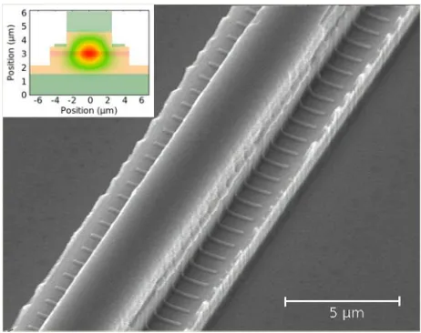
the sidewalls to prevent shorting of the cascades by metal grating stripes accidentally overlapping the shoulder edges. The 1st order grating with a duty cycle of 23% was then defined in PMMA resist on the shoulders of the lower ridge using e-beam lithography, followed by evaporation of Cr with a thickness of 110 nm. The period of the grating was varied between 864 nm and 912 nm. A scanning electron microscope image of the ridge after this step is shown in Figure 1. Afterwards, 200 nm Si3N4and 200 nm SiO2
passi-vation layers were sputtered onto the sidewalls. Following the removal of the passivation on top of the inner ridge, a Ti/ Pt/Au top contact was evaporated, and an additional 5lm of gold was electroplated on top for improved heat dissipation. After thinning the substrate to around 150lm, an AuGe/Ni/ Au bottom contact was evaporated. Subsequently, laser bars were cleaved from the sample and mounted epi-side up on copper heatsinks using In solder. The facets were left uncoated.
The measurements on the 45lm wide and 2 mm long RWG devices revealed a pulsed threshold current density of 950 A/cm2at a temperature of 20C. This is lower than our results published previously on 11 cascade ICLs grown on InAs substrates in this wavelength region,21which is mainly attributed to better carrier rebalancing in the electron injector due to the higher doping. The spectral characterization yielded emission around a central wavelength of 6.12lm at 20C. Laser emission could be measured up to a temperature of 49C.
[image:3.612.58.289.53.236.2]In Figure2, the light-current-voltage (L-I-V) character-istics of a narrow ridge Fabry-Perot device with a ridge width of 6lm and a resonator length of 2.4 mm in cw opera-tion in the temperature range between 16C and 0C are presented. With a maximum operation temperature of 0C, this marks the highest operation temperature of an InAs-based ICL in this wavelength range. Higher operation tem-peratures, even above room temperature, have only been reported below 5lm so far.11An emission spectrum of this FIG. 1. Scanning electron microscope image of the double ridge structure
after patterning of the chromium grating. The inset shows an overlay of the simulated mode profile and a cross-section of the waveguide.
device recorded at a temperature of16C is depicted in the inset.
Figure 3shows emission spectra recorded from a DFB device at a driving current of 260 mA at temperatures of 20C,15C, and10C. The dimensions of the device are 2.4 mm in length and 5.3lm and 9.3lm in width for the upper and lower ridge, respectively. The grating has a period of 875 nm. For the two lower temperatures, side mode sup-pression ratios (SMSR) of more than 30 dB can be observed, while for the spectrum recorded at10C, the side modes are buried under the noise originating from the FTIR mea-surement. No single mode emission could be measured above this temperature. Using the Bragg condition kDFB¼ 2nef fK with the grating period K and the emission wave-length of the device, an effective refractive index of 3.37 can be evaluated at 20C. This value compares well to our simulations of the waveguide structure.
The current dependent tuning behavior of the spectral mode of this device is depicted in Figure4for temperatures of 20C, 15C, and 10C. Tuning coefficients of 0.011 nm/mA with current and 0.50 nm/C with temperature
were extracted for this ridge. These values are slightly lower than those reported for a GaSb-based ICL-DFB emitting at 5.2lm.17A total tuning bandwidth of 6.5 nm, corresponding to 1.9 cm1, can be covered by this ridge in the temperature range from20C to10C.
Figure5shows the tuning behavior of another ridge with a grating period of 895 nm and a single mode emission around 6021 nm. The dimensions of this device are 3 mm5.3lm/ 9.3lm. Due to a low signal level at a temperature of10C, the signal to noise ratios were below 20 dB for these spectra, although the device was still working in cw operation. The degradation in device performance compared to the shorter wavelength ridge indicates a stronger heating of the structure with the drive current. This is supported by a much higher current-tuning coefficient of 0.024 nm/mA while the tempera-ture tuning coefficient of 0.49 nm/C stays nearly constant. This is likely to be caused by a higher thermal transfer resist-ance between the sample and the copper mount due to varia-tions in the mounting of the samples. The inset in Figure 5
[image:4.612.316.560.53.227.2]shows L-I-V characteristics of the second ridge at a tempera-ture of22C. A threshold current of 201 mA and a power FIG. 2. Light-current-voltage characteristics of a narrow ridge Fabry-Perot
device with a ridge width of 6lm and a length of 2.4 mm in cw operation at several temperatures. The device operates in the cw regime up to a tempera-ture of 0C. The inset shows an emission spectrum of this device at a tem-perature of16C.
FIG. 3. Emission spectra of a DFB device at temperatures of 20C,
15C, and10C. The spectra were recorded at a driving current of
[image:4.612.55.297.55.227.2]260 mA (device dimensions: 2.4 mm5.3lm/9.3lm).
[image:4.612.317.557.554.725.2]FIG. 4. Current dependent tuning characteristics for a 2.4 mm long and 5.3lm/9.3lm wide ridge with a grating period of 875 nm at temperatures of 20C,15C, and10C.
FIG. 5. Current dependent tuning characteristics for a 3.0 mm long and 5.3lm/9.3lm wide ridge with a grating period of 895 nm at temperatures of 20C and15C. The inset shows LI-V characteristics of this device at
[image:4.612.52.296.564.733.2]consumption at threshold of 726 mW have been measured. The latter compares very well to values reported just recently for QCL-DFBs emitting at surrounding wavelengths for devi-ces with uncoated facets and comparable lengths.22However, for short devices with optimized facet coatings, values as low as 310 mW at30C were reported at an emission wave-length of 5.25lm.
As both shown DFB devices emit rather at the edges of the gain region (see the inset in Figure 2), even better per-formances would be expected from devices emitting closer to the center of the gain. Unfortunately, no such lasers could be measured due to a low yield of working devices.
In conclusion, we realized a single mode emission from 11-stage InAs-based ICL-DFB devices based on a lateral metal grating. The narrow ridge devices showed laser emis-sion in cw operation up to temperatures of 0C. To fulfill the requirements for both, sufficient grating confinement and inhibited current spreading in the active region, a double ridge configuration was examined. In this configuration, the grating is placed above the active region on both sides of a shallowly etched ridge and a second, slightly wider, deeply etched ridge provides the current confinement. SMSRs above 30 dB have been measured in cw operation in the tempera-ture range between20C and 10C. With wavelengths up to 6024 nm in the single mode operation, we have demon-strated the longest wavelength ICL DFB.
We acknowledge the financial support from the European Commission in the frame of the FP7 project “WideLase” (Grant No. 318798). We would also like to thank S. Kuhn, A. Wolf, and M. Wagenbrenner, for assistance during sample preparation, growth, and characterization and R. Weih for fruitful discussions.
1
A. Bauer, K. R€oßner, T. Lehnhardt, M. Kamp, S. H€ofling, L. Worschech, and A. Forchel,Semicond. Sci. Technol.26, 014032 (2011).
2I. Vurgaftman, R. Weih, M. Kamp, J. R. Meyer, C. L. Canedy, C. S. Kim,
M. Kim, W. W. Bewley, C. D. Merritt, J. Abell, and S. H€ofling,J. Phys. D 48, 123001 (2015).
3R. Q. Yang, “Interband cascade (IC) lasers,” Semiconductor Lasers: Fundamentals and Applications, edited by A. Baranov and E. Tournie (Woodhead Publishing Limited, Cambridge, 2013), pp. 487–513.
4
R. Q. Yang,Superlattices Microstruct.17(1), 77 (1995).
5J. Scheuermann, R. Weih, M. V. Edlinger, L. N€ahle, M. Fischer, J. Koeth,
M. Kamp, and S. H€ofling,Appl. Phys. Lett.106, 161103 (2015).
6
I. Vurgaftman, W. W. Bewley, C. L. Canedy, C. S. Kim, M. Kim, C. D. Merritt, J. Abell, and J. R. Meyer,IEEE J. Sel. Top. Quantum Electron. 19, 1200210 (2013).
7C. L. Canedy, J. Abell, C. D. Merritt, W. W. Bewley, C. S. Kim, I.
Vurgaftman, J. R. Meyer, and M. Kim,Opt. Express22, 7702 (2014).
8
W. W. Bewley, C. L. Canedy, C. S. Kim, M. Kim, C. D. Merritt, J. Abell, I. Vurgaftman, and J. R. Meyer,Opt. Express20, 3235 (2012).
9Z. Tian, R. Q. Yang, T. D. Mishima, M. B. Santos, R. T. Hinkey, M. E.
Curtis, and M. B. Johnson,Electron. Lett.45, 48 (2009).
10
M. Dallner, F. Hau, S. H€ofling, and M. Kamp,Appl. Phys. Lett. 106, 041108 (2015).
11L. Li, Y. Jiang, H. Ye, R. Q. Yang, T. D. Mishima, M. B. Santos, and M.
B. Johnson,Appl. Phys. Lett.106, 251102 (2015).
12
J. S. Yu, S. Slivken, A. Evans, L. Doris, and M. Razeghi,Appl. Phys. Lett. 83, 2503 (2003).
13G. Boehm, S. Katz, R. Meyer, and M.-C. Amann,J. Cryst. Growth 311, 1932 (2009).
14
J. L. Bradshaw, J. D. Bruno, J. T. Pham, D. E. Wortman, S. Zhang, and S. R. J. Brueck,IEEE Proc. Optoelectron.150, 288 (2003).
15C. S. Kim, M. Kim, W. W. Bewley, J. R. Lindle, C. L. Canedy, J. Abell, I.
Vurgaftman, and J. R. Meyer,Appl. Phys. Lett.95, 231103 (2009).
16
C. S. Kim, M. Kim, J. Abell, W. W. Bewley, C. D. Merritt, C. L. Canedy, I. Vurgaftman, and J. R. Meyer,Appl. Phys. Lett.101, 061104 (2012).
17M. von Edlinger, J. Scheuermann, R. Weih, C. Zimmermann, L. N€ahle, M.
Fischer, J. Koeth, S. H€ofling, and M. Kamp, IEEE Photonics Technol. Lett.26, 480 (2014).
18R. Weih, L. N€ahle, S. H€ofling, J. Koeth, and M. Kamp,Appl. Phys. Lett.
105, 071111 (2014).
19
S. Forouhar, C. Borgentun, C. Frez, R. M. Briggs, M. Bagheri, C. L. Canedy, C. S. Kim, M. Kim, W. W. Bewley, C. D. Merritt, J. Abell, I. Vurgaftman, and J. R. Meyer,Appl. Phys. Lett.105, 051110 (2014).
20I. Vurgaftman, W. W. Bewley, C. L. Canedy, C. S. Kim, M. Kim, C. D.
Merritt, J. Abell, J. R. Lindle, and J. R. Meyer, Nat. Commun.2, 585 (2011).
21M. Dallner, M. Kamp, and S. H€ofling,Electron. Lett.49, 286 (2013). 22A. Bismuto, S. Blaser, R. Terazzi, T. Gresch, and A. Muller,Opt. Express
23, 5477 (2015).