Technical Review of Low
Dropout Voltage Regulator
Operation and Performance
August 1999
Mixed Signal Products
Application
Report
IMPORTANT NOTICE
Texas Instruments and its subsidiaries (TI) reserve the right to make changes to their products or to discontinue any product or service without notice, and advise customers to obtain the latest version of relevant information to verify, before placing orders, that information being relied on is current and complete. All products are sold subject to the terms and conditions of sale supplied at the time of order acknowledgement, including those pertaining to warranty, patent infringement, and limitation of liability.
TI warrants performance of its semiconductor products to the specifications applicable at the time of sale in accordance with TI’s standard warranty. Testing and other quality control techniques are utilized to the extent TI deems necessary to support this warranty. Specific testing of all parameters of each device is not necessarily performed, except those mandated by government requirements.
CERTAIN APPLICATIONS USING SEMICONDUCTOR PRODUCTS MAY INVOLVE POTENTIAL RISKS OF DEATH, PERSONAL INJURY, OR SEVERE PROPERTY OR ENVIRONMENTAL DAMAGE (“CRITICAL APPLICATIONS”). TI SEMICONDUCTOR PRODUCTS ARE NOT DESIGNED, AUTHORIZED, OR WARRANTED TO BE SUITABLE FOR USE IN LIFE-SUPPORT DEVICES OR SYSTEMS OR OTHER CRITICAL APPLICATIONS. INCLUSION OF TI PRODUCTS IN SUCH APPLICATIONS IS UNDERSTOOD TO BE FULLY AT THE CUSTOMER’S RISK.
In order to minimize risks associated with the customer’s applications, adequate design and operating safeguards must be provided by the customer to minimize inherent or procedural hazards.
TI assumes no liability for applications assistance or customer product design. TI does not warrant or represent that any license, either express or implied, is granted under any patent right, copyright, mask work right, or other intellectual property right of TI covering or relating to any combination, machine, or process in which such semiconductor products or services might be or are used. TI’s publication of information regarding any third party’s products or services does not constitute TI’s approval, warranty or endorsement thereof.
Contents
1 Dropout Voltage . . . 1
1.1 Application Implications. . . 4
2 Quiescent Current or Ground Current . . . 5
2.1 Application Implications. . . 6
3 LDO Topologies. . . 7
3.1 Application Implications. . . 9
4 Efficiency . . . 9
4.1 Application Implications—An Example . . . 9
5 Load Regulation . . . 10 5.1 Application Implications. . . 11 6 Line Regulation . . . 12 6.1 Application Implications. . . 13 7 Transient Response . . . 14 7.1 Application Implications. . . 14 8 Frequency Response. . . 16
9 Range of Stable ESR (Tunnel of Death) . . . 18
9.1 Application Implications. . . 20
10 Accuracy. . . 20
10.1 Reference Voltage Drift. . . 20
10.2 Error Amplifier Voltage Drift . . . 22
10.3 Tolerance of External Sampling Resistors. . . 22
10.4 Application Implications—an Example. . . 23
Figures
List of Figures
1. LDO Voltage Regulator. . . 1
2. Series Pass Element I-V Characteristic and LDO Equivalent Circuits . . . 2
3. NMOS Operation With LDO in Saturation Region . . . 3
4. NMOS Operation With LDO in Dropout Region . . . 3
5. Typical Input/Output Voltage Characteristics of a Linear Regulator . . . 4
6. Dropout Region of TI TPS76333 (3.3-V LDO) . . . 4
7. I-V Characteristic of Bipolar Transistors . . . 5
8. I-V Characteristic of MOS Transistors . . . 6
9. Quiescent Current and Output Current . . . 6
10. Linear Regulator . . . 7
11. Pass Element Structures . . . 7
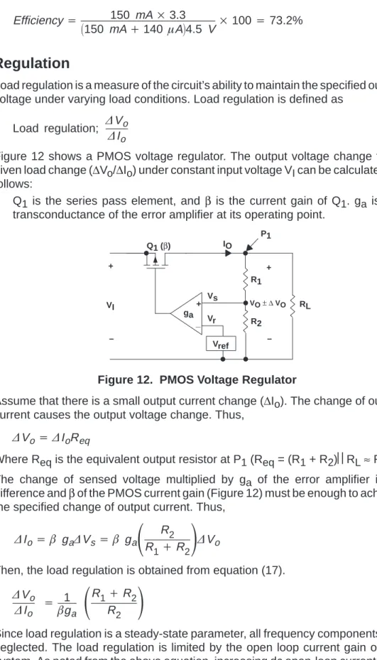
12. PMOS Voltage Regulator . . . 10
13. Load Transient Response of TPS76350 . . . 11
14. TPS76350 Output Voltage With Respect to Output Current . . . 11
15. Line Transient Response of TPS76333. . . 13
16. TPS76333 Output Voltage With Respect to Input Voltage . . . 13
17. 1.2-V, 100-mA LDO Voltage Regulator With Output Capacitor of 4.7 µF . . . 14
18. Transient Response of Step Load Change of 1.2-V, 100-mA LDO Voltage Regulator With an Output Capacitor Co=4.7 µF . . . 15
19. AC Model of a Linear Regulator . . . 16
20. Frequency Response of the LDO Voltage Regulator . . . 17
21. LDO Frequency Response Without Compensation. . . 18
22. LDO Frequency Response With External Compensation . . . 18
23. Unstable Frequency Response of LDO With too High ESR . . . 19
24. Unstable Frequency Response of LDO With too Low ESR . . . 19
25. Range of Stable ESR Values. . . 20
26. LDO With Reference Voltage Drift . . . 21
27. LDO With Error Amplifier Voltage Drift. . . 22
28. LDO With Sampling Resistors. . . 23
29. LDO Regulator . . . 24
List of Tables
1 Comparison of Pass Element Structures . . . 9Technical Review of Low Dropout Voltage Regulator Operation
and Performance
Bang S. Lee
ABSTRACT
This application report provides a technical review of low dropout (LDO) voltage regulators, and describes fundamental concepts including dropout voltage, quiescent current, and topologies. The report also includes detailed discussions of load/line regulation, efficiency, frequency response, range of stable ESR, and accuracy of LDO voltage regulators.
1
Dropout Voltage
Dropout voltage is the input-to-output differential voltage at which the circuit ceases to regulate against further reductions in input voltage; this point occurs when the input voltage approaches the output voltage. Figure 1 shows an example of a simple NMOS low dropout (LDO) voltage regulator.
Series Pass Element RO Id G + _ Control Circuit S D VO Vds Vi + _ + _
Figure 1. LDO Voltage Regulator
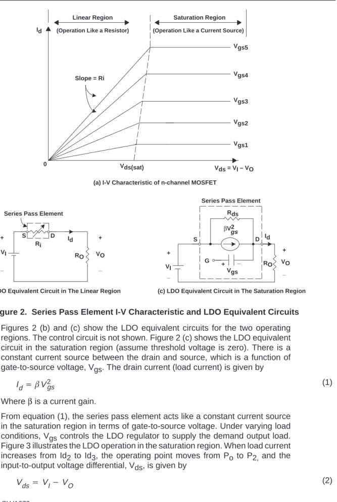
LDO operation can be explained using the NMOS series pass element I-V characteristics shown in Figure 2. NMOS devices are not widely used in LDO designs, but they simplify the explanation of LDO performance. Figure 2 (a) shows the two regions of operation—linear and saturation. In the linear region, the series pass element acts like a series resistor. In the saturation region, the device becomes a voltage-controlled current source. Voltage regulators usually operate in the saturation region.
Dropout Voltage
(Operation Like a Current Source)
Slope = Ri
0
Linear Region Saturation Region
Vgs5
(Operation Like a Resistor)
(b) LDO Equivalent Circuit in The Linear Region VI
Series Pass Element
S D G + Id gs βV2 _ Series Pass Element
S D Vgs4 Vgs3 Vgs2 Vgs1 Vds(sat) Vds = VI – VO Id Ri Id VO RO Rds VO VI Vgs RO
(a) I-V Characteristic of n-channel MOSFET
(c) LDO Equivalent Circuit in The Saturation Region + _ + _ + _ + _
Figure 2. Series Pass Element I-V Characteristic and LDO Equivalent Circuits
Figures 2 (b) and (c) show the LDO equivalent circuits for the two operating regions. The control circuit is not shown. Figure 2 (c) shows the LDO equivalent circuit in the saturation region (assume threshold voltage is zero). There is a constant current source between the drain and source, which is a function of gate-to-source voltage, Vgs. The drain current (load current) is given by
Id+ bV2gs
Where β is a current gain.
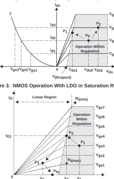
From equation (1), the series pass element acts like a constant current source in the saturation region in terms of gate-to-source voltage. Under varying load conditions, Vgs controls the LDO regulator to supply the demand output load. Figure 3 illustrates the LDO operation in the saturation region. When load current increases from Id2 to Id3, the operating point moves from Po to P2, and the input-to-output voltage differential, Vds, is given by
Vds+VI*VO
(1)
Dropout Voltage
From equation (2) and Figure 3, as the input voltage decreases, the voltage regulator pushes the operating point toward P1 (toward the dropout region). As the input voltage nears the output voltage, a critical point exists at which the voltage regulator can not maintain a regulated output. The point at which the LDO circuit begins to lose loop control is called the dropout voltage. Below the dropout voltage, the LDO regulator can no longer regulate the output.
0 Id3 Vgs4 β V(Dropout) P0 Operation Within Regulation P2 P1 Vgs3 Vgs2 Vgs1 Vds = VI – VO Vds0 Vds1 Vds2 Id2 Id1 Vgs1 Vgs3Vgs2 Vgs Ids
Figure 3. NMOS Operation With LDO in Saturation Region
Ri(max) 0 Pto Linear Region IO1 Vgs7 P3 V1 Vds = VI – VO Vgs6 Vgs5 Vgs4 Vgs3 Vgs2 Vgs1 P1 P2 V2 V3 IO Ri(min) Operation Within Regulation
Figure 4. NMOS Operation With LDO in Dropout Region
In the dropout region, the series pass element limits the load current like a resistor—as shown in Figure 2 (b). Figure 4 shows NMOS operation with the LDO regulator in the dropout region and decreasing input voltage. The equivalent resistors Ri(max) and Ri(min) are the maximum and minimum values respectively of the series pass element in the linear region. When the input voltage decreases to near the output voltage, the operating point P1 moves to the operating point P2 that is the minimum regulating point at the specific load condition (Io1) (i.e., dropout voltage). Within the dropout region, Vgs is not a function of the control loop, but of the input voltage. In other words, the regulator control loop cut off and
Dropout Voltage
voltage decreases further, the control voltage (Vgs) also decreases in proportion to the decreasing input voltage. The operating point moves down to P3 from P2. Finally, the regulator reaches the turnoff point, Pto.
Dropout Region Off Region VI V(dropout) [V] Vds VO Regulation Region
Figure 5. Typical Input/Output Voltage Characteristics of a Linear Regulator
Figure 5 shows the dropout region in relation to the off and regulation regions. Below V(dropout) , the output voltage drops with decreasing input voltage.
1.1
Application Implications
In dropout region, the magnitude of the dropout voltage depends on the load current and the on resistance (Ron) of the series pass element. It is given by
Vdo+ILoadRon
Throughout the dropout region, the output voltage is not maintained any more by the control loop since the control loop is electrically disconnected at the output of the controller (Figure 1) and then the pass device acts like a resistor. Therefore, the output voltage can be pulled down to ground by the load.
Figure 6 shows the input-output characteristics of the TPS76333 3.3-V LDO regulator. The dropout voltage of the TPS76333 is typically 300 mV at 150 mA. The LDO regulator begins dropping out at 3.6-V input voltage; the range of the dropout region is between 3.6 V and 2.0 V input voltage.
3.3 3.6 10 VI – input voltage – V 2.0 0 Dropout Region Off
Region RegulationRegion
– Output V
oltage – V
VO
Figure 6. Dropout Region of TI TPS76333 (3.3-V LDO)
Quiescent Current or Ground Current
2
Quiescent Current or Ground Current
Quiescent current, or ground current, is the difference between input and output currents. Minimum quiescent current is necessary for maximum current efficiency. Quiescent current is defined by
Iq+II*IO
Quiescent current consists of bias current (such as band-gap reference, sampling resistor and error amplifier) and drive current of the series pass element, which do not contribute to output power. The value of quiescent current is mostly determined by the series pass element, topologies, ambient temperature, etc.
Linear voltage regulators usually employ bipolar or MOS transistors as the series pass element. The collector current of bipolar transistors is given by
Ic+ bIb
where β is forward current gain and typically ranges from 20-500, Ic is the collector current, and Ib is the base current. Figure 7 shows the I-V characteristic of bipolar transistors. Vce 0 β Ib4 Ic Ic3 Ic2 Ic1 Ib3 Ib2 Ib1
Ib3 Ib2 Ib1 Ib
Figure 7. I-V Characteristic of Bipolar Transistors
Equation (5) and Figure 7 show that the base current of bipolar transistors is proportional to the collector current. As load current increases, base current also increases. Since base current contributes to quiescent current, bipolar transistors intrinsically have high quiescent currents. In addiiton, during the drop out region the quiescent current can increase due to the addiitional parasitic current path between the emitter and the base of the bipolar transistor, which is caused by a lower base voltage than that of the output voltage.
The drain-source current of MOS transistors is given by
Ids+ b1
ǒ
Vgs*VtǓ
2where β1 is a MOS transistor gain factor, Vgs is the gate-to-source voltage, and
Vt is the device threshold. Figure 8 shows the I-V characteristic of MOS
transistors.
(4)
(5)
Quiescent Current or Ground Current 0 1 β Ids Vgs4 Vds Vgs Vgs3 Vgs2 Vgs1 Ids4 Ids3 Ids2 Vgs4 Vgs3 Vgs2
Figure 8. I-V Characteristic of MOS Transistors
The drain-to-source current is a function of the gate-to-source voltage, not the gate current. Thus, MOS transistors maintain a near constant gate current regardless of the load condition.
2.1
Application Implications
Figure 9 shows the quiescent current of both transistors with respect to the load current. Bipolar Transistor MOS Transistor Iq IO 0 Standby Current
Figure 9. Quiescent Current and Output Current
For bipolar transistors, the quiescent current increases proportionally with the output current because the series pass element is a current-driven device. For MOS transistors, the quiescent current has a near constant value with respect to the load current since the device is voltage-driven. The only things that contribute to the quiescent current for MOS transistors are the biasing currents of band-gap, sampling resistor, and error amplifier. In applications where power consumption is critical or where small bias current is needed in comparison with the output current, an LDO voltage regulator employing MOS transistors is essential.
LDO Topologies
3
LDO Topologies
The regulator circuit can be partitioned into four functional blocks: the reference, the pass element, the sampling resistor, and the error amplifier as shown in Figure 10. Pass Element + _ + VDO _ IO VO Is Ir Ia II VI Idrv Vref + _ + _
Figure 10. Linear Regulator
Figure 11 shows that linear voltage regulators can be classified based on pass element structures: NPN-Darlington, NPN, PNP, PMOS, and NMOS regulators. The bipolar devices can deliver the highest output currents for a given supply voltage. The MOS-based circuits offer limited drive performance with a strong dependence on aspect ratio (width to length ratio) and to voltage-gate drive. On the positive side, however, the voltage-driven MOS devices minimize quiescent current flow. + Vsat + 2VBE – VDO – + + Vsat + VBE – – VDO + Ib – VDO + Idrv – VDO + + VGS – – VDO + Vsat – + (a) Darlington (b) NPN (c) PNP (e) NMOS (d) PMOS
Figure 11. Pass Element Structures
The Darlington requires at least 1.6 V of dropout voltage to regulate, while the LDO will typically work with less than 500 mV of input-to-output voltage differential. The dropout voltage of NPN-Darlington is given by
LDO Topologies
The NPN regulator is comprised of an NPN and a PNP transistor. The base potential of the NPN transistor should always be higher than the emitter potential to ensure proper operation of the pass element. When the input-output differential voltage is high, there is no problem. When the input voltage approaches the output voltage, the control circuit pushes the pass element toward saturation to ensure proper operation of the regulator, and the value of the transistor equivalent variable resistor decreases. However, the equivalent variable resistor can not decrease to zero because the transistor NPN needs to maintain a necessary Vbe level. Below a certain level of input voltage, the regulator cannot maintain the regulation.
The minimum voltage difference between the input and output required to maintain regulation (dropout voltage) is given by
V(dropout)+VCE(sat))VBEw0.9 V for NPN regulator
The NPN transistor receives its drive current from the input rail through the PNP transistor. The base drive circuit contributes its emitter current (Idrv) to output current (IO). Therefore, the quiescent current of the NPN regulator is small. The quiescent current for the NPN regulator is defined as follows:
Iq+Ibias for NPN regulator
Where:
Iq = quiescent current
Ibias = total bias current (Ibias = Ia + Ir + Is)
The PNP regulator shown in Figure 11 (c) operates the same as the NPN with the exception that the NPN pass transistor has been replaced by a single PNP transistor. The big advantage of the PNP regulator is that the PNP pass transistor can maintain output regulation with very little voltage drop across it.
V(dropout)+VCE(sat)^0.15X0.4 V for PNP regulator
By selecting a high-gain series transistor, dropout voltages as low as 150 mV at 100 mA are possible. However, the base drive current flows to ground and no longer contributes to the output current. The value of this ground current directly depends on the pass element transistor’s gain. Thus, the quiescent current of the PNP regulator is higher than the NPN regulator. The quiescent current is defined as follows:
Iq+Idrv)Ibias^0.8X2.6 mA for PNP regulator
Where:
Idrv = base drive current of PNP
Figures 11(d) and 11(e) show the P-MOS and N-MOS voltage regulators respectively, which employ MOSFETs as the pass element. The PMOS devices have very low dropout voltages. The NMOS can have a low dropout voltage with a charge pump. The dropout voltage is determined by saturation voltage across the pass element, and the dropout voltage is proportional to the current flowing through the pass element.
V(dropout)+IoRon^35X350 mV for PMOS regulator
(8)
(9)
(10)
(11)
Efficiency
where Ron is the on-resistance of the pass element
At light load, the dropout voltage is only a few millivolts. At full load, the typical dropout voltage is 300 mV for most of the families. The MOSFET pass element is a voltage controlled device and, unlike a PNP transistor, does not require increased drive current as output current increases. Thus, very low quiescent current is obtained (less than 1 mA).
3.1
Application Implications
Table 1 summarizes the differences of these pass element devices.[2]
Table 1. Comparison of Pass Element Structures
PARAMETER DARLINGTON NPN PNP NMOS PMOS
Io,max High High High Medium Medium
Iq Medium Medium Large Low Low
Vdropout Vsat+2Vbe Vsat+Vbe Vce(sat) Vsat+Vgs VSD(sat) Speed Fast Fast Slow Medium Medium
Traditionally, the PNP bipolar transistor has been applied to low dropout applications, primarily because it easily enables a low drop out voltage. However, it has a high quiescent current and low efficiency, which are not ideal in applications where maximizing efficiency is a priority. The NMOS pass element is most advantageous due to its low on resistance. Unfortunately, the gate drive difficulties make it less than ideal in applicaitons and as a result there are few NMOS LDOs available. PMOS devices have been highly developed and now have performance levels exceeding most bipolar devices.
4
Efficiency
The efficiency of a LDO regulator is limited by the quiescent current and input/output voltage as follows:
Efficiency+ IoVo
ǒ
Io)IqǓ
VI100
To have a high efficiency LDO regulator, drop out voltage and quiescent current must be minimized. In addition, the voltage difference between input and output must be minimized since the power dissipation of LDO regulators accounts for the efficiency
ǒ
Power Dissipation+ǒ
VI*VOǓ
IOǓ
. The input/output voltage difference is an intrinsic factor in determining the efficiency regardless of the load condition.4.1
Application Implications—An Example
What is the efficiency of the TPS76333 3.3-V LDO regulator with the following operating conditions?
•
Input voltage range is 3.8 V to 4.5 V.•
Output current range is 100 mA to 150 mA.•
Maximum quiescent current is 140 µA.Load Regulation
Efficiency+ǒ 150 mA 3.3
150 mA)140 mAǓ4.5 V 100+73.2%
5
Load Regulation
Load regulation is a measure of the circuit’s ability to maintain the specified output voltage under varying load conditions. Load regulation is defined as
Load regulation; DVo
DIo
Figure 12 shows a PMOS voltage regulator. The output voltage change for a given load change (∆Vo/∆Io) under constant input voltage VI can be calculated as follows:
Q1 is the series pass element, and β is the current gain of Q1. ga is the transconductance of the error amplifier at its operating point.
+ + – – + _ P1 IO R1 R2 VO ±∆ VO RL ga Vs Vr VI Q1 (β) Vref
Figure 12. PMOS Voltage Regulator
Assume that there is a small output current change (∆Io). The change of output current causes the output voltage change. Thus,
DVo+ DIoReq
Where Req is the equivalent output resistor at P1 (Req = (R1 + R2)RL ≈ RL).
The change of sensed voltage multiplied by ga of the error amplifier input
difference and β of the PMOS current gain (Figure 12) must be enough to achieve the specified change of output current. Thus,
DIo+ b gaDVs+ b ga
ǒ
R2R1)R2
Ǔ
DVoThen, the load regulation is obtained from equation (17).
DVo DIo + 1 bga
ǒ
R1)R2 R2Ǔ
Since load regulation is a steady-state parameter, all frequency components are neglected. The load regulation is limited by the open loop current gain of the system. As noted from the above equation, increasing dc open-loop current gain improves load regulation.
(14)
(15)
(16)
(17)
Load Regulation
5.1
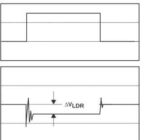
Application Implications
The worst case of the output voltage variations occurs as the load current transitions from zero to its maximum rated value or vice versa. Figure 13 shows that the load regulation is determined by the ∆VLDR. Figure 14 shows the output voltage variation with respect to the output current with the TPS76350 5-V LDO regulator. 0 100 200 150 100 0 –100 –150 t – Time – µs 0 50 100 150 ∆VLDR Output Current – mA Output V oltage Change – mV I O
Figure 13. Load Transient Response of TPS76350
50 0 30 0 60 90 120 150 180 IO – Output Current – mA 25 Output V oltage V ariation – mV
Line Regulation
6
Line Regulation
Line regulation is a measure of the circuit’s ability to maintain the specified output voltage with varying input voltage. Line regulation is defined as
Line regulation; DVo
DVI
The output voltage change for a given input voltage change (∆Vo / ∆VI) can be calculated from Figure 12 as follows;
Vo+ VIReq Rds)Req* DVo+ VIReq Rds)Req* DIoReq + VIReq Rds)Req*GǒVs*VrǓReq
where the open loop current gain G = β × ga, and Rds is the equivalent resistor between drain and source of the series pass element. Req is the equivalent output resistor at the point P1 (Req = (R1 + R2)RL ≈ RL). The sensed voltage Vs is given by
Vs+ R2
R1)R2Vo
Substituting (21) into equation (20),
Vo+
Req
ǒ
R1)R2Ǔ
Rds)Req VI)
ǒ
R1)R2Ǔ
GVrReqR1)R2)GR2Req Now in the usual case,
GVsơ1
From equations (22) and (23), the output voltage is
Vo+
ǒ
R1)R2Ǔ
GR2
ǒ
Rds)ReqǓ
VI)
ǒ
R1)R2Ǔ
R2 Vr
Now, the right hand side of the equation can be split into two parts. One is the steady state average output voltage and the another is the function of input voltage. The average steady state output voltage is then given by
Vo+
ǒ
R1)R2Ǔ
R2 Vr
Thus, the line regulation is obtained from equation (24).
DVo DVI + 1
ǒ
Rds)RLǓ
ǒ
R1)R2Ǔ
GR2 (19) (20) (21) (22) (23) (24) (25) (26)Line Regulation
Or substituting the open loop current gain G into equation (26), the line regulation can be DVo DVI +
ȧ
ȡ
Ȣ
ǒ
Rds)1RLǓ
bgaȧ
ȣ
Ȥ
ǒ
R1)R2 R2Ǔ
Like load regulation, line regulation is a steady state parameter—all frequency components are neglected. Increasing dc open loop current gain improves the line regulation.
6.1
Application Implications
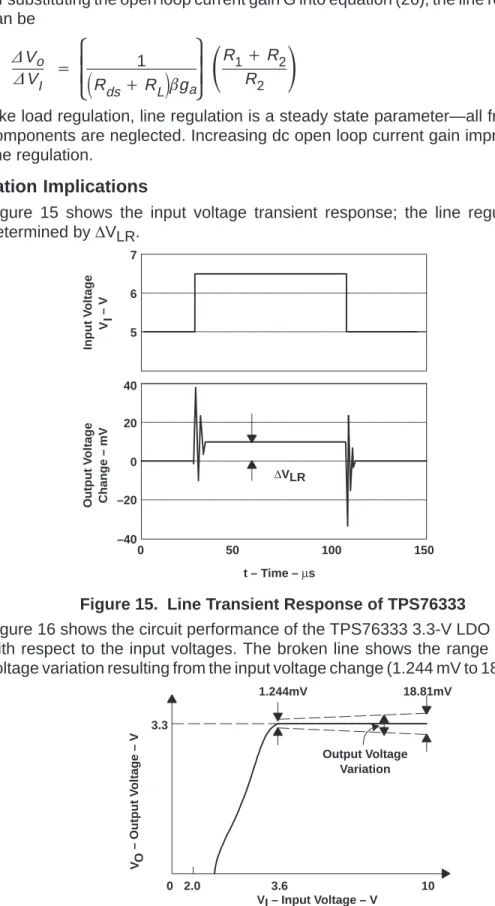
Figure 15 shows the input voltage transient response; the line regulation is determined by ∆VLR. 5 6 7 40 20 0 –20 –40 0 50 100 150 t – Time – µs Input V oltage – V Output V oltage Change – mV VI ∆VLR
Figure 15. Line Transient Response of TPS76333
Figure 16 shows the circuit performance of the TPS76333 3.3-V LDO regulator with respect to the input voltages. The broken line shows the range of output voltage variation resulting from the input voltage change (1.244 mV to 18.81 mV).
1.244mV 18.81mV 3.3 3.6 10 VI – Input Voltage – V 2.0 Output Voltage Variation 0 VO – Output V oltage – V
Figure 16. TPS76333 Output Voltage With Respect to Input Voltage
Transient Response
7
Transient Response
The transient response is an important specification, which is the maximum allowable output voltage variation for a load current step change. The transient response is a function of the output capacitor value (Co), the equivalent series resistance (ESR) of the output capacitor, the buypass capacitor (Cb), and the maximum load-current (Io,max). The application determines how low this value should be. The maximum transient voltage varitation is defined as follows[2].
DVtr, max+ Io,max
Co)Cb Dt1) DVESR
Where ∆t1 corresponds to the closed loop bandwidth. ∆VESR is the voltage variation resulting from the presence of the ESR (RESR) of the output capacitor.
∆VESR is proportional to RESR.
7.1
Application Implications
A LDO voltage regulator with output capacitor of 4.7 µF is shown in Figure 17.
Vref + _ Co = 4.7 µF RESR RL VI LDO regulator VO + _ Cb + _
Figure 17. 1.2-V, 100-mA LDO Voltage Regulator With Output Capacitor of 4.7 µF
Figure 18 illustrates the transient response of a 1.2 V, 100 mA LDO regulator with an output capacitor of 4.7 µF shown in Figure 17. A step change of load current (near 90 mA) was applied to the regulator which is shown in the upper trace of the figure. It is noted that in the lower trace the output voltage drops approximately 120 mV and then the voltage control loop begins to respond to the step load change in 1 µs (∆t1 = 1 µs). Finally, the output voltage reaches to a stble state
within 17 µs. From equation 28, the calculated maximum voltage variation is
given by:
DVtr, max+ 90 mA
4.7 mF)0 1 ms) DVESR +19 mV) DVESR+120 mV
Therefore, the output voltage variation of 101 mV is caused by the ∆VESR. The
effects of ∆VESR can be reduced by adding bypass capacitors shown in
Figure 17, which normally exhibit low ESR value.
To decrease the voltage variation resulting from the load transient, a big value of output capacitor and the low ESR of the capacitor are recommended. However, the Tunnel of Death (discussed in section 9) limits the values of output capacitor and its ESR value.
(28)
Transient Response Output Current 50 mA/div 1.2 V Output 50 mV/div (AC Coupled) ∆Vtr, max ∆t1
Figure 18. Transient Response of Step Load Change of 1.2-V, 100-mA LDO Voltage Regulator With an Output Capacitor Co=4.7 µF
Frequency Response
8
Frequency Response
Figure 19 shows the essential elements of a linear regulator.[2] The error amplifier is modeled by a transconductor (ga) with a load comprised of capacitor Cpar and resistor Rpar. The series pass element (MOS transistor) is modeled by a small signal model with transconductance gp. An output capacitor Co with an equivalent series resistor (RESR) and a bypass capacitor Cb is added.
+
_
Series Pass Element
LDO Z o S D G Vgs gp Vgs Rds gp R2 R1 VO RESR CO Cb Vref Cpar Rpar VI ga IL + _ + _
Figure 19. AC Model of a Linear Regulator
From Figure 19, the output impedance is given by
Zo+R12p
Ŧ
ǒ
RESR) 1 SCoǓ
Ŧ
1 SCb + R12pǒ
1)SRESRCoǓ
S2R 12pRESRCoCb)Sƪ
ǒ
R12p)RESRǓ
Co)R12pCbƫ
)1 Where R12p+RdsŦ
ǒ
R1)R2Ǔ
[RdsTypically, the output capacitor value Co is considerably larger than the bypass capacitor Cb. Thus, the output impedance Zo approximates to
Zo[ Rds
ǒ
1)SRESRCoǓ
ƪ
1)Sǒ
Rds)RESRǓ
Coƫ
ƪ
1)Sǒ
RdsŦ
RESRǓ
Cbƫ
From equation (32), a part of the overall open-loop transfer function for the regulator is obtained, and the zero and poles can be found. The first pole is
Po; S
ǒ
Rds)RESRǓ
Co+ *1 Therefore, ƒpo+ *1 2pǒ
Rds)RESRǓ
Co ] *1 2pRdsCoǒ
Because RdsơRESRǓ
(30) (31) (32) (33)Frequency Response
The second pole is obtained from equation (32) again, Pb; S
ǒ
RdsøRESRǓ
Cb+ *1 Therefore, ƒpb+ *1 2pǒ
RdsŦRESRǓ
Cb[ *1 2pRESRCb The zero is ZESR; SRESRCo+–1 Therefore, ƒZ(ESR)+ *1 2pRESRCoIn addition, another pole exists from the input impedance of the pass element (i.e. the output impedance of the amplifier, Rpar, Cpar). The approximated poles and the zero are then given by
Po[ 1 2pRdsCo[ IL 2pVACo Pb[ 1 2pRESRCb Pa[ 1 2pRparCpar and ZESR[ 1 2pRESRCo Where Rds[ VA IL , VA+ 1
l for MOS device, λ is the channel-length modulation
parameter. Pole Pa is the only one introduced at the input of the pass device, not at the output of the device. Figure 20 illustrates the typical frequency response of the LDO voltage regulator.
f – Frequency – Hz 0 –2 x x o x –2 Po –1 Pb Zesr –1 Gain – dB Pa
Figure 20. Frequency Response of the LDO Voltage Regulator
(34) (35) (36) (37) (38) (39) (40) (41)
Range of Stable ESR (Tunnel of Death)
9
Range of Stable ESR (Tunnel of Death)
An LDO regulator would require an output capacitor with an output equivalent series resistor (ESR) to stabilize the control loop. An LDO has two poles that can cause oscillations as shown in Figure 21 if it is not compensated. It is obvious that the linear regulator is unstable because the phase shift at unity gain frequency (UGF) is –180° due to the effects of two poles (Po, Pa) at low frequencies. To make the regulator stable, a zero must be added, which will cancel out the phase effect of one of two poles.
x x UGF 0 –2 Po –1 Gain – dB Pa f – Frequency – Hz
Figure 21. LDO Frequency Response Without Compensation
The equivalent series resistance of the output capacitor (ESR) or a compensated series resistor (CSR) is used for the zero. Figure 22 shows how the ESR (or CSR) zero stabilizes the control loop. The zero produced by the ESR locates before the UGF so that the phase shift at UGF1 will be around –90° (i.e., two poles –zero = -180°+90° = -90°). Thus, the linear regulator becomes stable. The phase shift of the control loop at UGF should always be less than –180° for system stability.
x x o x UGF UGF1 f – Frequency – Hz 0 –2 Po –1 Pb Zesr Gain – dB Pa –1
Range of Stable ESR (Tunnel of Death)
The ESR value should be maintained in the range that determines the loop stability. For most LDO regulators, minimum and maximum ESR values exist. Figures 23 and 24 show the unstable loop responses of an LDO regulator even though a zero is added. From equation (39) and (41), the zero Zesr and the pole
Pb are determined by the equivalent series resistor (ESR). When the ESR
changes, Zesr and Pb are shifted upward/downward and the loop stability is affected. x x –1 o x –2
Stable Region of ESR
f – Frequency – Hz 0 Po –1 Pb Zesr Gain – dB Pa –2
Figure 23. Unstable Frequency Response of LDO With too High ESR
Figure 23 illustrates the unstable frequency response of an LDO when too high an ESR is added, and Figure 24 illustrates the LDO frequency response when too low an ESR is used. For both cases, the total phase shift at unity gain frequency is –180°, resulting in system instability. The broken line in Figures 23 and 24 shows the stable range of Zesr.
x x o x –1 –2
Stable Region of ESR
0 Po –1 Pb Zesr Gain – dB Pa –2 f – Frequency – Hz
Accuracy
9.1
Application Implications
Since ESR can cause instability, LDO manufacturers typically provide a graph showing the stable range of ESR values. Figure 25 shows a typical range of ESR values with respect to the output currents. This curve is called tunnel of death. The curve shows that the ESR must be between 0.2 Ω and 9 Ω. Solid tantalum electrolytic, aluminum electrolytic, and multilayer ceramic capacitors are all suitable, provided they meet the ESR requirements.
10 100 1 0.1 0.01 0 50 100 150 200 250 Co = 4.7 µF IO – Output Current – mA Region of Instability Stable Region Region of Instability
Output Capacitor ESR –
Ω
Figure 25. Range of Stable ESR Values
10
Accuracy
Accuracy specifies all effects of line regulation (∆VLR), load regulation
(∆VLDR),reference voltage drift (∆Vo,ref), error amplifier voltage drift (∆Vo,a), external sampling resistor tolerance (∆Vo,r), and temperature coefficient (∆VTC). It can be defined by Accuracy[
Ť
DVLRŤ
)Ť
DVLDRŤ
) DV2 o,ref) DV 2 o,a) DV2o,r) DV2TCǸ
Vo 100Output voltage variation in a regulated power supply is due primarily to temperature variation of the constant voltage reference source and temperature variation of the difference amplifier characteristics as well as the sampling resistor tolerance. Load regulation, line regulation, gain error, and offsets normally account for 1% to 3% of the overall accuracy.
Output voltage variations resulting from the reference voltage drift, error amplifier voltage drift, and sampling resistor tolerance that are due to inter-lot and process variations are detailed in this section.
10.1
Reference Voltage Drift
Assume the LDO regulator exhibits the reference voltage drift (Vd) as shown in Figure 26. The reference voltage drift directly causes the output voltage change
(∆Vo,ref).
Accuracy Reference + _ R1 R2 VO + ∆Vo, ref RL ga Vs Vr ± Vd VI Q1 (β) + _ + _
Figure 26. LDO With Reference Voltage Drift
Thus, the resultant output voltage is
Vo) DVo,ref+
ƪ
Vs–ǒ
Vr"VdǓ
ƫ
gabRLThe sensed voltage Vs is given by
Vs+
R2
R1)R2
ǒ
Vo) DVo,refǓ
Substituting equation (44) into equation (43),
Vo) DVo,ref+
ƪ
R2
R1)R2
ǒ
Vo) DVo,refǓ
*ǒ
Vr"VdǓ
ƫ
gabRL+
ǒ
R1)R2Ǔǒ
–Vr#VdǓ
gabRLR1)R2–R2gabRL Now in the usual case,
gabVsơ1
From equation (45) and (46), the output voltage is obtained.
Vo) DVo,ref+
R1)R2
R2
ǒ
Vr"VdǓ
Now, the right hand side of the equation can be split into two parts. One is the average output voltage and the other is the function of the reference voltage drift. The average output voltage is then given by
Vo+
ǒ
R1)R2Ǔ
R2 Vr
Thus, the output voltage variation resulting from reference voltage drift is obtained from equation (47).
DVo,ref+R1)R2
R2
ǒ
"VdǓ
From equations (48) and (49), the following equation is obtained.
DVo,ref VO +" Vd Vr (43) (44) (45) (46) (47) (48) (49) (50)
Accuracy
Equation (50) shows that the output voltage variation is directly affected by the accuracy of the reference voltage. If the reference voltage accuracy is 1%, then the output voltage of the regulator will exhibit the same percentage of variation.
10.2
Error Amplifier Voltage Drift
The error amplifiers exhibit drift characteristics with temperature. Assume that an error (or drift) voltage Vd appears at the output of the amplifier as shown in Figure 27. + _ R1 R2 VO ±∆VO, a RL ga ±Vd Vr VI Q1(β) Vref Vs + _ + _
Figure 27. LDO With Error Amplifier Voltage Drift
The output change ∆Vo,a resulting from the drift voltage Vd is obtained from Figure 27.
DVo,a+ bVdRL"gabDVsRL
The sensed voltage ∆Vs is given by
DVs+
R2
R1)R2 DVo,a
Substituting equation (52) into equation (51)
DVo,a+
bVd
ǒ
R1)R2Ǔ
RL R1)R2"gabR2RLBy equation (46), the output voltage variation resulting from the error amplifier voltage drift is obtained as follows.
DVo,a+"
Vd
ǒ
R1)R2Ǔ
gaR210.3
Tolerance of External Sampling Resistors
For adjustable regulators, the output depends on the accuracy of two sampling resistors. Suppose that the sampling resistors of an LDO regulator have tolerances such as ±∆R1 and ±∆R2 as shown in Figure 28.
(51)
(52)
(53)
Accuracy + _ R1 ±∆R1 VO ±∆ VO, r RL ga Vs Vr VI Q1(β) Vref R2 ±∆R2 + _ + _
Figure 28. LDO With Sampling Resistors
The output voltage change resulting from the sampling resistor tolerance is Vo) DVo,r+gab(Vs–Vr)RL
The sensed voltage Vs is given by
Vs+
ǒ
R2" DR2Ǔ
ǒ
R1" DR1Ǔ
)ǒ
R2" DR2Ǔ
ǒ
Vo) DVo,rǓ
Substituting Vs into equation (55)Vo) DVo,r+
–gabVr
ƪ
ǒ
R1" DR1Ǔ
)ǒ
R2" DR2Ǔ
ƫ
RLǒ
R1" DR1Ǔ
)ǒ
R2" DR2Ǔ
–gabǒ
R2" DR2Ǔ
RLBy equation (46), the output voltage resulting from the tolerance of the sampling resistors is obtained as follows.
Vo) DVo,r+
ǒ
R1" DR1Ǔ
)ǒ
R2" DR2Ǔ
ǒ
R2" DR2Ǔ
Vr Thus, the average output voltage is given byVo+
R1)R2 R2" DR2 Vr
The average output voltage is a function of the resistor accuracy. Specifically, the bottom side of the resistor dominates the overall LDO accuracy. The output voltage variation due to the resistor tolerance is given by.
DVo,r+"
DR1) DR2 R2" DR2 Vr
10.4
Application Implications—an Example
What is the total accuracy of the 3.3-V LDO regulator shown in Figure 29 over the temperature span from 0° to 125° with the following operating characteristics?
•
Temperature coefficient is 100 ppm/°C.•
Sampling resistor tolerance is 0.25%.•
Output voltage change resulting from load regulation, and line regulation are±5 mV, and ±10 mV, respectively. (55) (56) (57) (58) (59) (60)
Accuracy
•
Accuracy of the reference is 1%.+ _ R R VO RL ga Vs Vref VI Q1 (β) Vref + _ + _
Figure 29. LDO Regulator
The output voltage is given by
Vo+R)R
R Vref+2 Vref
Therefore, the reference voltage Vref is half of the output voltage (i.e. Vref = 3.3/2[V]), and
DVTC+Temperature Coefficient
ǒ
Tmax*TminǓ
Vo+(100 ppmń°C) (125°C) (3.3 V) + 41.2 mV
DVo,r+(0.25% of Vo)0.25% of Vo) Vref
+(0.005) (3.3) 3.3
2 +27 mV
From equation (49), the output voltage variation resulting from the reference voltage is obtained as follows.
DVo,ref+2
ǒ
3.32
Ǔ
0.01+33 mVWhere
Vd+Vref 0.01+
ǒ
3.32
Ǔ
0.01Therefore, the overall accuracy of the LDO is obtained as follows,
Accuracy[10 mV)5 mV) (33 mV) 2 )(27 mV)2)(41.2 mV)2
Ǹ
3.3 V 100[2.25% (64) (61) (62) (63)References
11
References
1. Adel S. Sedra and K.C. Smith, Microelectronic Circuits, Oxford Univ. Press, June 1997
2. Gabriel Alfonso Rincon-Mora, Current Efficient, Low Voltage, Low Drop-Out Regulators, Ph.D Thesis, Georgia Institute of Technology, November 1996. 3. P.R. Gray and R.G.Meyer, Analysis and Design of Analog Integrated Circuits,
New York; John Wiley & Sons, Inc., 1993
4. Abraham I. Pressman,Switching and Linear Power Supply, Power Converter Design, Rochelle Park, New Jersey; Hayden Book Company, Inc., 1977 5. The Engineering Staff of Texas Instruments Semiconductor Group, The
Voltage Regulator Handbook, Dallas, Texas; Texas Instruments Incorporated, 1977


![Table 1 summarizes the differences of these pass element devices.[2]](https://thumb-us.123doks.com/thumbv2/123dok_us/1113033.2648130/13.918.169.797.340.445/table-summarizes-differences-pass-element-devices.webp)