Imperial College London
Department of Computing
Reconfigurable Architectures for
Cryptographic Systems
Adrien Le Masle
Submitted in partial fulfilment of the requirements for the degree of Doctor of Philosophy in Computing of Imperial College London
and the Diploma of Imperial College London
Declaration
I herewith certify that all material in this dissertation which is not my own work has been duly acknowledged.
Abstract
Field Programmable Gate Arrays (FPGAs) are suitable platforms for implementing cryp-tographic algorithms in hardware due to their flexibility, good performance and low power con-sumption. Computer security is becoming increasingly important and security requirements such as key sizes are quickly evolving. This creates the need for customisable hardware designs for cryptographic operations capable of covering a large design space. In this thesis we explore the four design dimensions relevant to cryptography – speed, area, power consumption and security of the crypto-system – by developing parametric designs for public-key generation and encryption as well as side-channel attack countermeasures. There are four contributions.
First, we present new architectures for Montgomery multiplication and exponentiation based on variable pipelining and variable serial replication. Our implementations of these architectures are compared to the best implementations in the literature and the design space is explored in terms of speed and area trade-offs.
Second, we generalise our Montgomery multiplier design ideas by developing a parametric model to allow rapid optimisation of a general class of algorithms containing loops with depen-dencies carried from one iteration to the next. By predicting the throughput and the area of the design, our model facilitates and speeds up design space exploration.
Third, we develop new architectures for primality testing including the first hardware ar-chitecture for the NIST approved Lucas primality test. We explore the area, speed and power consumption trade-offs by comparing our Lucas architectures on CPU, FPGA and ASIC.
Finally, we tackle the security issue by presenting two novel power attack countermea-sures based on on-chip power monitoring. Our constant power framework uses a closed-loop control system to keep the power consumption of any FPGA implementation constant. Our attack detection framework uses a network of ring-oscillators to detect the insertion of a shunt resistor-based power measurement circuit on a device’s power rail. This countermeasure is lightweight and has a relatively low power overhead compared to existing masking and hiding countermeasures.
Acknowledgements
I would like to express my greatest gratitude to my supervisor Prof. Wayne Luk for pointing at the right direction and giving me invaluable guidance throughout my research at Imperial College London. I am grateful to my second supervisor Dr. Cristian Cadar for his insightful comments on my work.
I would like to acknowledge Gary Chow for his help on designing the constant power frame-work presented in chapter 6, in particular its proposed architecture for the power consumer.
I am grateful to Professor Csaba Andras Moritz for giving me invaluable support and sug-gestions on my work, as well as all the people at BlueRISC: Sylvia Moritz, Kris Carver, Jeff Gummeson, Felipe Vilas-Boas and Alan Boulanger.
I express my gratitude to my fellow colleagues in the Custom Computing Group of Imperial College London: Dr. Tobias Becker, Brahim Betkaoui, Thomas Chau, Kit Cheung, Gary Chow, Dr. Gabriel De Figueiredo Coutinho, Stewart Denholm, Dr. Andreas Fidjeland, Gordon Inggs, Maciej Kurek, Qiwei Jin, Nicholas Ng, Xinyu Niu, Dr. Timothy Todman, Dr. Anson Tse, and Dr. Brittle Tsoi for their friendly support.
I would like to thank my family and my long-time friends Aur´elie Villaume, Emilie Dupetit-magneux, Yoann Gasque, and J´erˆome Raymond for their love and encouragement.
Special thanks to all my UK friends for providing happiness and unforgettable memories to my PhD life, in particular: Nuri Purswani, Felipe Nascimento, Sofia Galligani, Sabine Wilke, Laith Sami, Magdalena Wiktoria Sliwinska, Ian Gladman, Cindy Bhagwandin, Florence Picoli, Tiffany Boutwood, Katy Evans, Joseph K. Ansah, Edward L. Albino Torres, and Kathleen Diane Gosling.
Contents
Declaration 3 Abstract 5 Acknowledgements 7 Contents 9 List of Figures 15 List of Tables 19 List of Algorithms 21 1 Introduction 23 1.1 Motivation . . . 23 1.2 Contributions . . . 25 1.3 Thesis organisation . . . 28 1.4 Publications . . . 29 2 Background 31 2.1 Field Programmable Gate Arrays (FPGAs) . . . 312.1.1 Device structure . . . 31
2.1.2 Tools . . . 33
2.1.3 Applications . . . 34
2.2.1 Principles . . . 36
2.2.2 Cryptanalysis and brute-force attacks . . . 38
2.2.3 Data Encryption Standard (DES) . . . 40
2.2.4 Advanced Encryption Standard (AES) . . . 43
2.3 Public-key cryptography . . . 48 2.3.1 Principles . . . 48 2.3.2 Requirements . . . 50 2.3.3 Key sizes . . . 51 2.3.4 RSA . . . 51 2.4 Side-channel attacks . . . 54
2.4.1 FPGA power consumption . . . 55
2.4.2 Power analysis . . . 57
2.4.3 Countermeasures . . . 59
2.5 Summary . . . 60
3 Parametric Montgomery Multiplier Architecture 61 3.1 Motivation . . . 61
3.2 Introduction to Montgomery Arithmetic . . . 62
3.2.1 Montgomery multiplication algorithm . . . 62
3.2.2 Hardware implementations of the Montgomery algorithm . . . 66
3.2.3 Montgomery modular exponentiation . . . 69
3.3 Scalable Montgomery multiplier architecture . . . 70
3.4 Application to modular exponentiation . . . 74
3.4.1 Basic Montgomery exponentiator . . . 74
3.4.2 Adding interleaved exponentiation support . . . 75
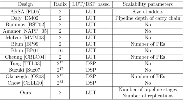
3.5 Design space exploration and comparison to existing architectures . . . 78
3.6 Summary . . . 86
4 Mapping Loop Structures onto Parametrised Hardware Pipelines 89 4.1 Motivation . . . 89
4.2 Main idea . . . 91
4.3 General bit by bit processing algorithm with loop-carried dependency . . . 93
4.4 Mapping of the algorithm to the parametric hardware description . . . 94
4.5 Modelling of the architecture . . . 98
4.5.1 Latency and throughput . . . 98
4.5.2 Frequency . . . 100
4.5.3 Area . . . 101
4.5.4 Constraints . . . 102
4.5.5 Throughput optimisation . . . 103
4.6 Optimising the design . . . 103
4.6.1 Determining the values of the parameters . . . 103
4.6.2 Design generation and optimisation process . . . 105
4.7 Accuracy and design space exploration results . . . 106
4.7.1 Accuracy of the model . . . 106
4.7.2 Design space exploration . . . 110
4.8 Summary . . . 111
5 Novel Architectures for Probabilistic Primality Testing 113 5.1 Motivation . . . 113
5.2 Probabilistic primality testing . . . 115
5.2.1 Fermat primality test . . . 115
5.2.2 Miller-Rabin primality test . . . 116
5.2.3 Lucas primality test . . . 117
5.2.4 Combining tests . . . 121
5.3 Miller-Rabin primality test architecture . . . 122
5.4 Lucas primality test . . . 123
5.4.1 Challenge 1: Jacobi symbol calculator . . . 125
5.4.2 Challenge 2: Lucas sequence calculator . . . 125
5.4.3 Challenge 3: scheduling . . . 128
5.5 Speed/Area/Power trade-off of FPGA and ASIC implementations . . . 131
5.5.1 FPGA implementation of our Miller-Rabin architecture . . . 131
5.5.2 FPGA and ASIC implementations of our Lucas architecture . . . 132
5.6 Summary . . . 136
6 Power Attacks Countermeasures Involving On-Chip Monitoring 139 6.1 Motivation . . . 139
6.2 Power attack measurement settings . . . 141
6.3 On-chip power monitoring with ring oscillators . . . 142
6.4 Constant power reconfigurable computing . . . 144
6.4.1 Principles . . . 144
6.4.2 On-chip power consumer . . . 147
6.4.3 Power controller . . . 147
6.4.4 Evaluation . . . 152
6.5 Detecting Power Attacks . . . 156
6.5.1 Principles . . . 156
6.5.2 Attack detection model . . . 157
6.5.3 Evaluation of the model . . . 162
6.5.4 Detection capabilities . . . 166
6.5.5 Alternative detection strategy . . . 172
6.6 Summary . . . 174
7 Conclusion and Future Work 175 7.1 Conclusion . . . 175
7.2 Future work . . . 179
7.2.1 Very low area end of the design space . . . 179
7.2.2 Power consumption model . . . 179
7.2.3 Speculative execution of Miller-Rabin tests . . . 180
7.2.4 Lucas instruction schedule . . . 180
7.2.6 Faster constant power control loop . . . 181
7.2.7 Improved attack detection . . . 181
Bibliography 183 A Proportional-Integral-Derivative (PID) Control 195 A.1 Algorithm . . . 195
A.2 Setpoint weighting . . . 197
A.3 Filtering . . . 197
A.4 Anti-windup . . . 198
A.5 Discretisation of the PID control algorithm . . . 198
A.6 PID control in our constant framework . . . 201
B Power Attacks on Reconfigurable Hardware 205 B.1 Comparative power attack against RSA . . . 205
B.1.1 Principles . . . 205
B.1.2 Phase Only Correlation (POC) waveform matching . . . 206
B.1.3 Implementation . . . 207
B.2 Differential power attack against DES . . . 208
B.2.1 Principles . . . 209 B.2.2 Implementation . . . 210 C Design Testing 213 C.1 Unit testing . . . 213 C.2 Integration testing . . . 213 D Experimental Parameters 217 D.1 Xilinx tools options . . . 217
D.1.1 Virtex-5 . . . 217
D.1.2 Spartan-6 . . . 218
D.2 Synopsys tools options . . . 219
D.2.2 45 nm . . . 220 D.3 Lucas test input for maximum execution time . . . 221
List of Figures
1.1 Organisation of this thesis . . . 28
2.1 Island-style architecture . . . 32
2.2 Simple logic element . . . 32
2.3 3-LUT configured as a 3-input XOR . . . 33
2.4 FPGA design flow . . . 35
2.5 Symmetric key encryption . . . 37
2.6 Stream and block ciphers . . . 38
2.7 16-round Feistel encryption and decryption . . . 41
2.8 DES encryption algorithm . . . 42
2.9 Calculation off(R, K) . . . 43
2.10 AES encryption algorithm . . . 45
2.11 Public-key encryption . . . 50
2.12 Public-key authentication . . . 50
2.13 CMOS NAND gate . . . 56
3.1 Montgomery multiplication with two ripple-carry adders . . . 66
3.2 Montgomery multiplication with one ripple-carry adder . . . 66
3.3 Montgomery multiplication with two CSAs . . . 68
3.4 Montgomery multiplication with one CSA . . . 68
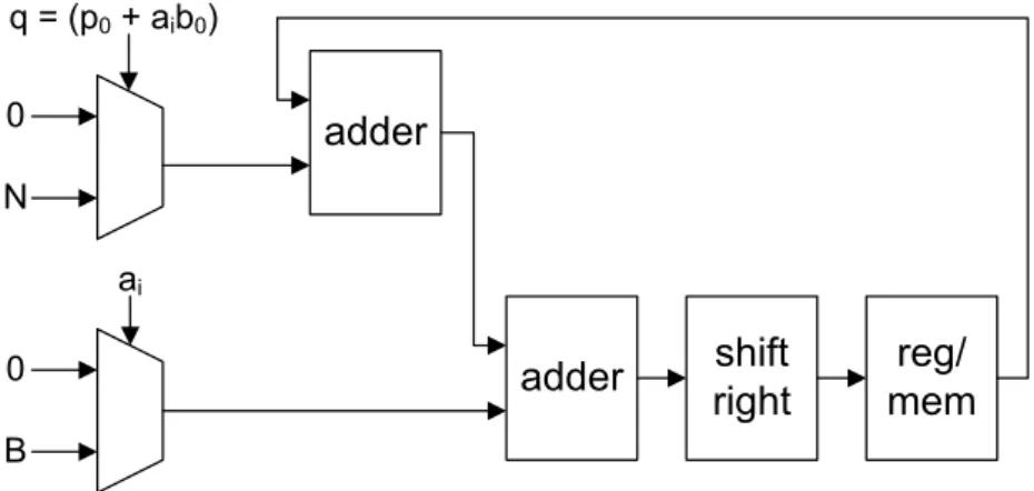
3.5 Diagram of a Montgomery multiplier cell . . . 71
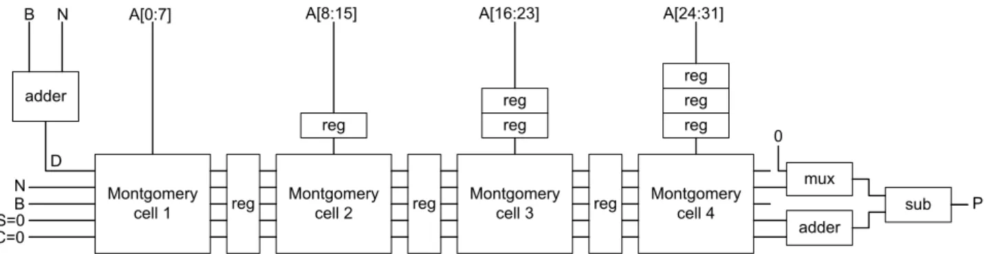
3.6 Structure of a 32 bit pipelined Montgomery multiplier with 4 pipeline stages . . 72
3.8 Montgomery exponentiator . . . 75
3.9 Modular exponentiations in a 4-stage pipeline . . . 76
3.10 Modular exponentiator with interleaved exponentiation support . . . 77
3.11 Multiplication latency after synthesis on a XC5VLX330T against p for different values of r . . . 82
3.12 Multiplication latency after synthesis on a XC5VLX330T against r for different values of p . . . 82
3.13 Multiplication throughput after synthesis on a XC5VLX330T against p for dif-ferent values of r . . . 82
3.14 Multiplication throughput after synthesis on a XC5VLX330T against r for dif-ferent values of p . . . 82
3.15 Area taken by our multiplier after synthesis on a XC5VLX330T against p for different values ofr . . . 83
3.16 Area taken by our multiplier after synthesis on a XC5VLX330T against r for different values ofp . . . 83
3.17 Exponentiation time after synthesis on a XC5VLX330T against r for different values of p . . . 85
3.18 Area taken by our exponentiator after synthesis on a XC5VLX330T against r for different values ofp . . . 85
4.1 Pipeline of the parametric hardware description . . . 96
4.2 Inside pipeline blocki . . . 96
4.3 Optimisation process . . . 105
5.1 Miller-Rabin prime tester . . . 124
5.2 Square root cell . . . 124
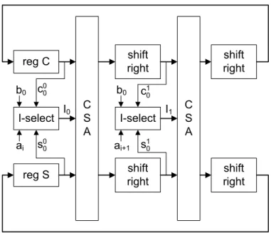
5.3 Hardware design for modular add-shift . . . 127
5.4 Analysis of the true dependencies in the Lucas sequence calculation algorithm . 129 5.5 Lucas sequence calculator schedule for a 3-stage multiplier’s pipeline . . . 129
6.2 Power monitor . . . 144
6.3 Constant-power framework . . . 145
6.4 Power control principle . . . 146
6.5 Power consumer . . . 146
6.6 Controller configuration sequence . . . 149
6.7 PID auto-tuning method . . . 149
6.8 Resolution of the attack against bandwidth . . . 156
6.9 Power attack detection framework . . . 157
6.10 Calibration and monitoring stages . . . 158
6.11 Calibration of a hardware core . . . 159
6.12 Operating conditions monitored by the attack detector . . . 161
6.13 Modified Pico E-101 FPGA board . . . 163
6.14 Frequency against supply voltage for each of the 128 ROs . . . 164
6.15 Oscilloscope power traces of modular exponentiation for different shunt resistor values REXT . . . 164
6.16 16-RO power monitor traces of modular exponentiation for different shunt resis-tor valuesREXT . . . 164
6.17 Amplitude of the shunt resistor voltage against the resistor value . . . 165
6.18 Amplitude of the power monitor reading against the resistor value . . . 165
6.19 ∆0pdistribution of 512-bit RSA for different number of ring oscillators and shunt resistor values . . . 168
6.20 ∆0pdistribution of 128-bit AES for different number of ring oscillators and shunt resistor values . . . 170
6.21 Power drop due to the attack detector for 64 ROs . . . 173
A.1 Simple PID control loop . . . 196
A.2 PID control loop with setpoint weighting, filtering and anti-windup . . . 199
A.3 Comparison of P, PI and PID controllers in our constant power framework . . . 201
A.4 RSA power trace without control . . . 202
A.6 RSA power trace with PI controller . . . 202
A.7 RSA power trace with PID controller . . . 202
B.1 Doubling attack . . . 206
B.2 Comparison of the POC functions . . . 208
B.3 Power trace of a DES encryption . . . 211
B.4 Result of the DPA attack against DES . . . 212
C.1 Verilog code for the CSA . . . 214
C.2 Wrapper for testing the CSA with MyHDL . . . 214
List of Tables
1.1 Summary of our research contributions . . . 27
2.1 Types of attacks . . . 39
3.1 Comparison of hardware implementations of Montgomery multiplication . . . 69
3.2 Performance comparison of 1024 bit multipliers . . . 80
3.3 Latency×Area and Area / Throughput normalised to our best designs for 1024 bit multiplication . . . 81
3.4 Performance comparison of 1024 bit exponentiators . . . 84
3.5 Time ×Area product normalised to our best design for 1024 bit exponentiation 84 4.1 Parameters of the general algorithm . . . 93
4.2 Specialisation of the general algorithm for three applications . . . 95
4.3 Determination of the design parameters . . . 104
4.4 Application-dependent parameters for our three applications . . . 108
4.5 Design parameters obtained after pre-synthesis . . . 108
4.6 Accuracy of our model . . . 109
4.7 Evaluation of prediction capabilities of the model . . . 109
4.8 Design constraints . . . 110
5.1 Performance comparison of 1024 bit Miller-Rabin . . . 132
5.2 Time× Area product normalised to our best design for 1024 bit Miller-Rabin test132 5.3 FPGA implementation results of 1024 bit Lucas primality testers . . . 133
6.1 Detected attacks (% of total runs - of which % of high voltage detections) . . . . 169 6.2 Attack detector power overhead for 512-bit RSA . . . 169
7.1 Summary of the key results . . . 178 7.2 Summary of limitations of this thesis and possible future work . . . 182
List of Algorithms
2.1 AES encryption algorithm . . . 44
2.2 AES decryption algorithm . . . 47
3.1 Montgomery reduction algorithm . . . 63
3.2 Radix-r Montgomery modular multiplication algorithm . . . 64
3.3 Radix-2 Montgomery modular multiplication algorithm . . . 65
3.4 Right-to-left binary exponentiation algorithm . . . 70
3.5 Carry-save Montgomery algorithm for modular multiplication . . . 71
4.1 General bit by bit processing algorithm . . . 93
5.1 Generation of large prime numbers . . . 114
5.2 Fermat primality test . . . 115
5.3 Miller-Rabin strong pseudoprime test . . . 116
5.4 Miller-Rabin strong pseudoprime test deterministic variant . . . 117
5.5 Simple Lucas test algorithm . . . 118
5.6 Lucas probabilistic primality test . . . 120
5.7 Binary integer square root algorithm . . . 122
5.8 Binary Jacobi algorithm . . . 126
5.9 Decomposition of the operations performed in the for loop of the Lucas primality test algorithm . . . 126
5.10 Modular addition with right shift . . . 127
Chapter 1
Introduction
1.1
Motivation
Field Programmable Gate Arrays (FPGAs) are suitable platforms for implementing crypto-graphic algorithms in particular, and computationally demanding applications in general – this field is known as reconfigurable computing. First, the structure of FPGAs makes them partic-ularly suitable for pipelined applications, which is the case for most of the basic cryptographic operations. Second, FPGAs can be used to embed security into low power environments keeping very good performance. Finally, a pure hardware implementation of a cryptographic algorithm is usually less vulnerable than its software counterparts which are usually run in a multi-tasking operating system.
FPGAs are quickly increasing in capability and in size, and it becomes a growing challenge to fully cover the design space available for a given budget and time to market. In parallel, as computer security is becoming increasingly important, protocols and security requirements are quickly evolving. For example an established algorithm may require increased key lengths to resist cryptanalytic attacks for a few more decades [NIS12]. How can we make use of the extra area provided by new devices or update a crypto-system with new security requirements without going through the whole design process? This question illustrates the need for parametric and customisable hardware designs for cryptographic operations capable of covering a large design space.
power consumption. The main advantages of parametric designs are their scalability and their reusability. They can be reused as IP cores in many projects with different trade-offs. However, finding the optimal values for the parameters to meet a given design goal can be difficult and time-consuming. An exhaustive approach implementing designs for all the values of the parameters in a given search interval cannot be achieved in most projects where the time-to-market is an issue. Therefore we need models that allow rapid optimisation of design parameters and facilitates design space exploration.
A fourth dimension to consider when specifically dealing with cryptographic applications is the security of the crypto-system (or its resistance to attacks). Attacks can be divided into two categories: attacks on the encryption scheme and attacks on the implementation. Encryption algorithms are designed to resist brute-force attacks and cryptanalysis, provided that a proper key size is chosen. Hence the strength of the encryption scheme relies on choosing an approved algorithm [ITLN09,NIS01] together with a suitable key size. The key size is chosen according to the time the information needs to be kept secret [NIS12]. However, the physical implementation of an encryption algorithm can leak information and create security flaws. Attacks exploiting these physical flaws are called side-channel attacks.
Since their initial publication [KJJ99], a type of side-channel attack called power attacks have been extensively studied. Power attacks recover the key of the encryption algorithm by using one or multiple power traces, which are directly correlated to the switching activity of the transistors inside the device. They have been successfully demonstrated on many common en-cryption methods, including private key enen-cryption such as DES [SOQP04] and AES [SMPQ06], finite field based public key encryption such as RSA [MDS99] and Diffie-Hellman, and elliptic curve based public key encryption [OOP03]. Theoretically, power attacks can be used to attack any crypto-system with key-dependent power consumption. Hence proper countermeasures against these attacks need to be incorporated and security of the implementation needs to be considered.
In this thesis we develop parametric designs for cryptographic applications. Our designs are especially useful for key generation and encryption in public-key cryptography. The design space is explored in terms of speed, area, power consumption and security. A technology-independent
parametric model is developed to allow rapid optimisation under speed and area constraints of a general class of algorithms, which include some of our cryptographic applications. Resistance to attacks is tackled by presenting two new power attack countermeasures based on on-chip power monitoring. The following section presents our contributions in more detail.
1.2
Contributions
The major contributions of this thesis are divided into the following parts. Our research con-tributions are also summarised in Table 1.1.
Parametric designs for public-key encryption
We present new hardware architectures for Montgomery modular multiplication and exponenti-ation. In order to explore a large design space in terms of speed-area trade-off, our Montgomery multiplier architecture uses variable pipeline stages and variable serial replications. Based on the multiplier architecture, we design a modular exponentiation circuit. Modular exponenti-ation is the main operexponenti-ation behind RSA encryption/decryption. We compare our designs to existing architectures and discuss their scalability. Our best multiplier is 13 times faster than the optimised software running on one core of a Core 2 Duo at 2.8 GHz, and is 4 times faster than the best hardware implementation in the literature. (Chapter 3)
Rapid optimisation of parametric designs
We generalise the idea used to scale our Montgomery multiplier. We present a coarse-grained method to automatically map a general class of algorithms consisting of a loop with loop depen-dencies carried from one iteration to the next to a parametric hardware design with pipelining and replication features. A technology-independent parametric model of the proposed design is developed to capture the variations of area and throughput with the number of pipeline stages and replications. Our model allows rapid optimisation of design parameters by a few pre-synthesis operations. We present an optimisation method based on the model. We show that our method facilitates design space exploration by quickly predicting the area taken by
the design as well as its maximum frequency and throughput. It is up to 96 times faster than a full search through the design space. (Chapter 4)
Novel architectures for primality testing
We present the first hardware architecture for the NIST approved Lucas primality test and an architecture for the Miller-Rabin primality test. Our architectures are based on our Mont-gomery multiplier and MontMont-gomery exponentiator. We introduce our Miller-Rabin architecture briefly before focusing on the Lucas primality test. We present a hardware architecture to com-pute the Jacobi symbol based on the binary Jacobi algorithm. We analyse the dependencies in the Lucas sequences computation and propose a schedule for the different operations. Finally we compare the performance of our Miller-Rabin and Lucas architectures with an optimised software implementation in terms of speed, area and energy efficiency. Our Lucas architectures are implemented on a Xilinx Virtex-5 FPGA, and also synthesized for TSMC 65 nm and 45 nm ASICs. The FPGA implementation is 5 times more energy efficient than the optimised software running on an Intel Xeon at 2.53 GHz. The 65 nm ASIC implementation is up to 39 times more energy efficient than the FPGA implementation. The 45 nm ASIC implementation is 420 times more energy efficient than the optimised software implementation. (Chapter 5)
Power attack prevention and detection using on-chip monitoring
We present a novel approach involving on-chip power monitoring to prevent power attacks on reconfigurable hardware. Our power monitor circuit is based on a network of evenly distributed ring-oscillators. Two power attack countermeasures are derived from this circuit. They both work under the assumption that an attacker uses a shunt resistor-based power measurement circuit to perform the attack. The first countermeasure is a general framework based on a closed-loop control system that keeps the power consumption of any FPGA implementation constant. We analyse this new idea and show that using the framework as a hiding countermeasure is not directly feasible on current commercial FPGAs. However it could be implemented as a hard IP block on an FPGA dedicated to cryptography. The second countermeasure involves detecting the insertion of a shunt resistor-based power measurement circuit onto a device’s
power rail. To our knowledge, this is the first attempt at detecting power attacks targeting reconfigurable hardware. This countermeasure is lightweight and has a relatively low power overhead. Shunt resistors as low as 2 Ω are detected with a maximum false-positive rate of 0.4% and no false-negatives. (Chapter 6)
Table 1.1: Summary of our research contributions
Research area Contributions
Parametric designs for public-key encryption (Chapter 3)
• New parametric Montgomery multiplier architecture using variable pipeline stages and variable serial replications.
• Montgomery exponentiation circuit based on our multiplier architecture with interleaved exponentiation support.
• Speed/area comparisons with existing architectures and scalability results.
Rapid optimisation of parametric
designs (Chapter 4)
• Coarse-grained method for mapping algorithms containing one loop with loop dependencies carried from one iteration to the next to a parametric design using pipelining and replication.
• Model of the design that allows predicting the throughput and area varia-tions with the number of pipeline stages and replicavaria-tions.
• General optimisation process integrating the model.
• Analysis of the accuracy and prediction capabilities of the optimisation method.
Primality testing architectures
(Chapter 5)
• The first hardware architecture for the NIST approved Lucas probabilistic primality test.
• Hardware architecture for computing the Jacobi symbol.
• Dependence analysis and scheduling of the Lucas sequence computation. • Comparison of our architectures on FPGA and ASIC with an optimised
software in terms of speed, area and energy efficiency.
Power attack prevention and detection
(Chapter 6)
• On-chip power monitor circuit based on a network of ring oscillators. • General framework based on a closed-loop control system that keeps the
power consumption of any FPGA implementation constant.
• Attack detection framework to detect the insertion of a shunt resistor-based power measurement circuit onto a device’s power rail.
• Implementation and in-depth evaluation of our constant power and attack detection frameworks.
1.3
Thesis organisation
This thesis is organised as follows. Chapter 2 introduces the general background relevant to our work. Chapter 3 presents a parametric Montgomery multiplier based on variable pipelining and serial replication and its application to modular exponentiation. Chapter 4 generalises the idea of the previous chapter by presenting a coarse-grained method to map loops with loop dependencies carried from one iteration to the next to a parametric hardware design. Chap-ter 5 presents novel architectures for probabilistic primality testing based on our Montgomery multiplication and exponentiation designs. Chapter 6 describes new power attack countermea-sures based on on-chip power monitoring using a network of ring oscillators. Finally chapter 7 summarises the contributions of this thesis and presents ideas for improvement and future work. The organisation of the thesis together with the research topics explored in each chapter are outlined in Fig. 1.1.
Chapter 1 -Introduction Chapter 2 -Background Chapter 3 -Parametric Montgomery Architectures Chapter 5 -Primality Testing Architectures Chapter 4 -Mapping Loops onto Hardware Pipelines Chapter 6 -Power Attacks Counter-measures Chapter 7 -Conclusion and Future Work Speed - Area Power Security
1.4
Publications
Journal Papers
1. Adrien Le Masle and Wayne Luk. Mapping Loop Structures onto Parametrised Hardware Pipelines. Submitted to IEEE Transactions on Very Large Scale Integration (VLSI)
Systems (under review).
2. Adrien Le Masle and Wayne Luk. Power Attack Countermeasures Involving On-Chip Power Monitoring. Submitted to IEEE Transactions on Computers (under review).
Conference Papers
1. Adrien Le Masle, Wayne Luk, Jared Eldredge, and Kris Carver. Parametric Encryp-tion Hardware Design. In ARC ’10: Proceedings of the 6th International Symposium on
Applied Reconfigurable Computing, 2010.
2. Adrien Le Masle and Wayne Luk. Design Space Exploration of Parametric Pipelined De-signs. InASAP ’10: Proceedings of the 21st IEEE International Conference on
Application-specific Systems, Architectures and Processors, 2010.
3. Adrien Le Masle, Wayne Luk, and Csaba Andras Moritz. Parametrized Hardware Ar-chitectures for the Lucas Primality Test. In SAMOS XI: Proceedings of the 11th In-ternational Conference on Embedded Computer Systems: Architectures, Modeling and
Simulation, 2011.
4. Adrien Le Masle, Gary C. T. Chow, and Wayne Luk. Constant Power Reconfigurable Computing. In FPT 2011: 2011 International Conference on Field-Programmable
Tech-nology.
5. Adrien Le Masle and Wayne Luk. Detecting Power Attacks on Reconfigurable Hard-ware. In FPL 2012: 2012 International Conference on Field Programmable Logic and
Chapter 2
Background
This chapter presents the general background relevant to our work. We first introduce Field Programmable Gate Arrays (FPGAs). Then we discuss the two main types of encryption schemes, namely symmetric-key and public-key cryptography. Finally, we present side-channel attacks and power attacks. Additional background material is given in each main chapter in order to facilitate their understanding.
2.1
Field Programmable Gate Arrays (FPGAs)
A Field Programmable Gate Arrays (FPGA) is a reconfigurable hardware device that can be programmed with any digital design after manufacturing. In this section we present the FPGA structure, the typical FPGA design flow and describe some FPGA applications. Extensive surveys of reconfigurable computing architectures and design methods are available in [Cha08, TCW+05].
2.1.1
Device structure
The three principal components of an FPGA are logic, interconnects and I/O blocks. In island-style FPGAs, logic, interconnects and I/O blocks are organised in a two-dimensional array as shown in Fig. 2.1. The logic blocks connect to the general programmable interconnects via SRAM-based programmable switch boxes (not shown in Fig. 2.1).
Logic Block Logic Block Logic Block Logic Block Logic Block Logic Block Logic Block Logic Block Logic Block Logic Block Logic Block Logic Block Logic Block Logic Block Logic Block Logic Block Programmable interconnects IO pads IO pads IO p ad s IO p ad s
Figure 2.1: Island-style architecture
a lookup table (LUT), a Flip-Flop (FF) and a multiplexer (MUX) as depicted in Fig. 2.2. The output of the LUT can be registered into the FF. The MUX selects either the output of the LUT or the output of the flip-flop.
Look Up Table
(LUT) Flip Flop (FF) MUX Output k inputs..
Figure 2.2: Simple logic element
A k-input LUT (k-LUT) can implement any logical function of k inputs by configuring 2k SRAM cells with the truth table of the function. An example of a 3-LUT performing a 3-input logical XOR is shown in Fig. 2.3. Complex functions can be implemented by combining LUTs together. Most modern FPGAs are based on 4-input or 6-input LUTs.
A logic block and a logic element are respectively called Configurable Logic Block (CLB) and Slice in Xilinx FPGA families [Xil11b] and Logic Array Block (LAB) and Adaptative Logic Module (ALM) in Altera FPGA families [Alt12]. In modern FPGAs logic elements contain
Figure 2.3: 3-LUT configured as a 3-input XOR
several LUTs, FFs and MUXes together with extra logic. The extra logic is often used for fast carry-chain addition or shift registers.
The logic element consisting of LUTs, FFs and extra logic is a fine-grained computation block. Most FPGAs contain a mix of such fine-grained blocks together with coarse-grained blocks such as Digital Signal Processors (DSPs) and memory elements. DSPs speed up opera-tions such as addiopera-tions and multiplicaopera-tions whereas embedded memory elements offer fast and low area-consuming storage.
As an example a Xilinx Spartan-6 contains two slices per CLB. Each slice contains four 6-LUTs, eight FFs and eight MUXes. In addition, one of the CLB slices contains extra logic for fast carry generation. In about half of the device’s CLBs, this slice also contains dis-tributed RAM and shift registers [Xil10a]. The Spartan-6 also contains several DSP blocks. The XC6SLX150T, which is the largest FPGA in the Spartan-6 family has 23 038 slices and 180 DSP blocks. Most recent FPGAs such as the Virtex-7 can reach more than 300 000 slices and 3000 DSP blocks [Xil12d].
2.1.2
Tools
The standard FPGA design flow is shown in Fig. 2.4. After specification, the design is pro-grammed in a Hardware Description Language (HDL). The most popular HDLs are Verilog and VHDL, which work at the Register-Transfer Level (RTL). Some approaches involving high level programming languages targeting hardware also exist. We can cite for example Handel-C [Gra10], Vivado High-Level Synthesis [Xil12a] and MaxHandel-Compiler [Tec11]. These high level
languages often generate RTL code. They usually speed up design time but are less flexible than standard HDLs. One way of verifying HDL designs is by behavioural testing. Testbenches are written in order to verify each component of the design. Then the design is synthesized. This step takes the RTL design and turns it into a logic gate netlist. After synthesis we obtain useful estimates of the area consumption and the speed of the design. The logic gate netlist is tested again usually using the same behavioural testbenches. The mapping process maps the logic gate netlist to FPGA primitives such as LUTs, FFs, RAMs and DSPs. If not enough resources are available on the device, the mapping fails and the user has to modify the RTL design. The place-and-route process takes user constraints, places the primitives and routes the design. User constraints are typically timing constraints and optional placement and routing constraints. The placer and router try to match these constraints and output a timing report. If the timing is not met, the user can choose to relax the constraints or to modify the HDL design. Post-place and route tests can be performed at that stage using accurate timing in-formation generated by the place-and-route process. Then the bitstream for the configuration SRAMs of the FPGA is generated. Finally the FPGA is programmed with the bitstream of the design which can be tested on chip. A common FPGA design cycle iterates through all these steps until a functional implementation meeting timing and area requirements is found.
2.1.3
Applications
The structure of an FPGA makes it naturally suited to parallel and pipelined applications. Many FPGA applications exist in a wide variety of areas such as networking [SP03], video processing [LAD+98], high-performance computing [HVG+07], software-defined radio [BLC09], industrial control systems [Liu11] and cryptography [BP99]. FPGAs can also be used as rapid-prototyping platforms for application-specific integrated circuits (ASICs) and microprocessors. ASICs are faster and consume less power than FPGAs. However, FPGAs have many advantages that can influence a designer to choose an FPGA over an ASIC implementation. In particular the time-to-market of a project using an FPGA is much shorter than the same project using an ASIC. As a matter of fact, unlike ASICs FPGAs are standard devices which have already been fabricated, packaged and tested by the vendor. FPGAs can also be less expensive than
Specifications
HDL design
Synthesis
Place & Route
Bitstream generation FPGA programming Behavioural tests Post-synthesis tests Post-Place & Route tests On-chip tests Mapping
Figure 2.4: FPGA design flow
ASICs, especially in lower volumes since no user-specific fabrication is involved.
FPGAs are suitable platforms for implementing cryptographic algorithms. First, the struc-ture of FPGAs makes them particularly suitable for pipelined applications, which is the case for most of the basic cryptographic operations. Second, FPGAs can be used to embed security into low power environments keeping very good performance. Finally, a pure hardware imple-mentation of a cryptographic algorithm is usually less vulnerable than its software counterparts which are usually run in a multi-tasking operating system.
2.2
Symmetric-key cryptography
In this section we give an overview of symmetric-key cryptography and we present the two most common symmetric-key encryption algorithms.
2.2.1
Principles
Generalities
Symmetric-key cryptography was the only encryption scheme until the invention of public-key cryptography in the 70s. It usually has five main components [Sta11, p. 57]:
• The plaintext P which is the non-encrypted message.
• The encryption algorithmE used to encrypt the plaintext by applying a set of substitu-tions and transformasubstitu-tions.
• The secret keyK used both for encryption and decryption. The operations performed by the algorithm depend on the key.
• The ciphertext C which is the encrypted message produced by the encryption algorithm.
• The decryption algorithmD used to decrypt the ciphertext using the secret key.
The main feature of symmetric-key cryptography is the use of the same keyK for encryption and decryption. The key has to be shared between the sender and the receiver in a secure way and must be kept safe. The encryption algorithm is often required to be designed so that an attacker having access to a number of ciphertexts together with the corresponding plaintexts cannot decrypt any other ciphertext and/or recover the key. Note that the security of a well-designed cryptographic system should not depend on the secrecy of the algorithm, but only on the secrecy of the key. In other words a cryptosystem should be secure even if everything about the system, except the key, is publicly available. This principle, known as Kerckhoffs’s principle, was stated by Auguste Kerckhoffs in 1883 [Ker83].
Encryption algorithm E Decryption algorithm D Symmetric key K Symmetric key K Output Plaintext P Input Plaintext P Ciphertext C Alice Bob
Figure 2.5: Symmetric key encryption
1. A secret key K is generated and shared between Alice and Bob over a secure channel. This can be done using public-key encryption, which is presented in section 2.3.
2. If Alice wants to send a confidential message P to Bob, Alice encrypts the message using the secret key K. The ciphertext is therefore:
C =E(K, P) (2.1)
3. After receiving the message, Bob can decrypt it using the same key K as follows:
P =D(K, C) (2.2)
The encryption process is summarised in Fig. 2.5.
Block Cipher and Stream Cipher
A block cipher is an encryption/decryption algorithm which processes a fixed-size plaintext block and produces a ciphertext block of the same size. Longer plaintexts/ciphertexts can be processed using several modes of operation (electronic codebook, cipher block chaining, cipher feedback mode, output feedback mode or counter mode, etc) approved by the National Institute of Standards and Technology (NIST) [NIS].
A stream cipher encrypts a data stream one bit or one byte at a time, usually combining the data stream with a cryptographic bit-stream. The cryptographic bit-stream is generated
Bit-stream generation algorithm Key (K) Cryptographic bit-stream (ki) Plaintext (pi) Bit-stream generation algorithm Key (K) Cryptographic bit-stream (ki) Ciphertext (ci) Plaintext (pi) Encryption Decryption
(a) Stream cipher
Encryption algorithm Key (K) Plaintext (P) Ciphertext (C) Encryption Decryption algorithm Plaintext (P) Decryption Key (K) (b) Block cipher
Figure 2.6: Stream and block ciphers (adapted from [Sta11, p. 93])
by a bit-stream generation algorithm using the secret key.
The differences between a block and a stream cipher are shown in Fig. 2.6. Widely used symmetric encryption algorithms such as DES and AES are all block ciphers.
2.2.2
Cryptanalysis and brute-force attacks
Cryptanalytic attacks exploit knowledge about the cryptographic algorithm and optionally some plaintexts or plaintext-ciphertext pairs, in order to recover a given plaintext or the se-cret key. Several types of cryptanalytic attacks exist according to how much information the attacker can obtain from the cryptographic system. The five main types of attacks are shown in Table 2.1.
In every case, we suppose that the attacker knows the encryption algorithm and has ac-cess to the ciphertext, which constitutes the ciphertext-only attack type. In a known-plaintext scenario, the attacker is able to capture some plaintext messages and their corresponding cipher-texts. A chosen-plaintext attack is possible if the attacker can encrypt any plaintext using the crypto-system. The chosen-ciphertext attack is the symmetric of the chosen-plaintext attack.
Table 2.1: Types of attacks (adapted from [Sta11, p. 60]) Attack type Additional information available to attacker
(encryption algorithm and ciphertext known by default) Ciphertext-only • None
Known-plaintext • Some plaintext-ciphertext pairs
Chosen-plaintext • Plaintext chosen by attacker and access to corresponding ci-phertext encrypted with secret key
Chosen-ciphertext • Ciphertext chosen by attacker and access to corresponding plaintext decrypted with secret key
Chosen-text
• Plaintext chosen by attacker and access to corresponding ci-phertext encrypted with secret key
• Ciphertext chosen by attacker and access to corresponding plaintext decrypted with secret key
The chosen-text attack assumes that the attacker can encrypt/decrypt any plaintext/cipher-text with the crypto-system and obtain the corresponding cipherplaintext/cipher-text/plainplaintext/cipher-text. Encryption algorithms are usually designed to withstand at least known-plaintext attacks.
Brute-force attacks enumerate every possible key until an intelligible plaintext is recovered from the ciphertext. For a key of size n, there are 2n possible keys. If n is large enough, such an attack is not computationally feasible in practice.
Two common definitions try to quantify the security of an encryption scheme [Sta11, p. 61]. We say that an encryption scheme is unconditionally secure if not enough information is present in the ciphertext to determine the plaintext, no matter how much ciphertext can be obtained. An unconditionally secure encryption algorithm must use keys with the same security requirements as the one-time pad. For each message, the one-time pad uses a new random key of the same length as the message for encryption and decryption. This scheme produces random ciphertexts with no statistical relationship to the corresponding plaintexts and is therefore unbreakable. However it is limited by the fact that creating a large quantity of truly random keys as well as distributing and protecting all these keys is impractical. Hence
none of the widely used encryption algorithms is unconditionally secure. An encryption scheme is computationally secure if the cost of breaking the cipher is higher than the value of the encrypted information, or if the time required to break the cipher is higher than the time the information needs to be kept secret. It can be hard to estimate whether a crypto-system is computationally secure. NIST gives recommended key sizes and lifetimes for their approved encryption ciphers [NIS12] in order to guide the design of a crypto-system.
2.2.3
Data Encryption Standard (DES)
Algorithm
The Data Encryption Standard (DES) is one of the best known symmetric-key encryption schemes. It was adopted in 1977 by the NIST [NIS99]. DES is a block cipher encrypting 64-bit blocks using a 56-bit key1. DES is based on a Feistel cipher structure that alternates between substitutions and permutations. The Feistel cipher structure is shown in Fig. 2.7. The data are divided into a right and a left half. Roundi takes the left part Li−1, the right part of the data Ri−1 and Ki as inputs. Ki is derived from the key K through a subkey generation algorithm. The output data are computed as:
Li =Ri−1 (2.3)
Ri =Li−1⊕f(Ri−1, Ki) (2.4)
A substitution is performed on the left halfLi−1 of the data by taking the exclusive or ofLi−1
with the round function f applied to the right half Ri−1 and the round key Ki. Then the two halves of the data are permuted. As shown in Fig. 2.7, the encryption and decryption processes are very similar. The ciphertext is decrypted by swapping its two halves and performing the same round operations using the round keys in reverse order. The output of these operations give the plaintext (with its left and right halves swapped).
The DES encryption algorithm is shown in Fig. 2.8. DES has 16 rounds following the Feistel structure with an extra permutation at the beginning and at the end. In the key schedule, the
LE0 RE0 f LE1 RE1 K1 f LE2 RE2 K2 f LE16 RE16 K16 LE15 RE15
.
.
.
Plaintext Ciphertext LD0=RE16 RD0=LE16 f LD1=RE15 RD1=LE15 K16 f LD2=RE14 RD2=LE14 K15 f LD16=RE0 RD16=LE0 K1 LD15=RE1 RD15=LE1.
.
.
Ciphertext PlaintextInitial permutation Round 1 Round 2 Round 16 Swap halves Inverse initial permutation Permuted choice 1
Left circular shift
Left circular shift
Left circular shift Permuted choice 2 Permuted choice 2 Permuted choice 2 64 64 64 64 64 64 48 48 48 56 56 56 64 56 56 K1 K16 K2 Plaintext Ciphertext Key Key schedule Encryption
Figure 2.8: DES encryption algorithm
64-bit key is initially truncated and permuted (Permuted choice 1) to obtain a 56-bit key. In each round the key is rotated using a predefined shift schedule. The shifted key is truncated to 48-bit and permuted again (Permuted choice 2) to form the round key Ki.
The Feistel function used for DES encryption/decryption is shown in Fig. 2.9. The 32-bit right half R is expanded to 48 bits using an expansion permutationE and combined with the 48-bit round key K using exclusive or. The 48-bit result is dispatched to a series of S-boxes
S1 to S8. Each S-box performs a substitution on a 6-bit input and returns a 4-bit output. Finally the 32-bit output of the set of S-box is permuted using a permutation functionP. The decryption algorithm is similar to the encryption algorithm with the key schedule performed in reverse order.
The operations of each permutations box, expansion box and S-box are defined precisely by the standard in [NIS99].
R K S1 E P S2 S3 S4 S5 S6 S7 S8 48 48 48 32 32 32 Figure 2.9: Calculation of f(R, K) Security
The relatively short key size of DES makes it vulnerable to brute-force attacks. In 1998, a custom machine that is able to crack DES in a few days for less than $250,000 was built by the Electronic Frontier Foundation [Fou98]. Since then much cheaper machines have been built such as the Copacobana machine made of 120 low-cost FPGAs that can break DES in less than nine days on average for $10,000 [KPP+06]. DES is still approved by NIST in the triple-DES mode, which uses a larger 112-bit key [NIS12]. However, in new applications DES is superseded by the Advanced Encryption Standard (AES).
2.2.4
Advanced Encryption Standard (AES)
The Advanced Encryption Standard (AES) was published by NIST in 2001 as a symmetric block cipher to replace DES [NIS01]. AES is not a Feistel cipher. In AES, all operations are performed on byte-wide data represented as polynomials over GF(28) with the irreducible
polynomial (x8+x4+x3+x+ 1). The plaintext block size is 128 bits and the key can be 128,
192 or 256 bits. The cipher consists of N rounds, depending on the key size: 10 rounds for a 128-bit key, 12 rounds for a 196-bit key and 14 rounds for a 256-bit key. A key expansion mechanism creates a round key for each of the N rounds. The round keys are always 128-bit
long for any of the three secret key sizes. In the first (N-1) rounds, four transformations are performed in the following order: SubBytes, ShiftRows, MixColumns, AddRoundKey.
An initial AddRoundKey transformation is performed before the first round. The last round consists only of three operations (SubBytes, ShiftRows, AddRoundKey). During the encryption/decryption process, the intermediate data (state) and the round keys are represented as 4x4 matrices of bytes. The state is initialised column by column with the 16-byte plaintext. The SubBytes, ShiftRows and MixColumns operations only take the state as inputs, whereas the AddRoundKey operation uses both the state and the round key. The final state is returned as the ciphertext. Each column of the state matrix is considered as a polynomial of degree 4 whose coefficients are finite field elements in GF(28). The AES encryption process is shown in
Fig. 2.10 and the encryption algorithm is shown in Algorithm 2.1.
In the following, we give an overview of each of the four AES transformations. These transformations as well as the key expansion mechanism are explained in more detail in [NIS01, Sta11].
Algorithm 2.1: AES encryption algorithm
Input: plaintext, roundkey, number of rounds ROU N DS
Output: ciphertext 1 state =plaintext
2 state =AddRoundKey(state, roundkey[0]) 3 for round= 1 to ROU N DS do
4 state=SubBytes(state) 5 state=Shif tRows(state)
6 if round < ROU N DS then state =M ixColumns(state) state=AddRoundKey(state, roundkey[round])
7 end
Initial transformation Round 1 (4 transformations) Round N-1 (4 transformations) Round N (3 transformations) K ey e xp an si on
Plaintext (16 bytes) Key (M bytes)
Input state (16 bytes) Key (M bytes) Round 0 key (16 bytes) Round 1 key (16 bytes) Round N-1 key (16 bytes) Round N key (16 bytes) Round 1 input state (16 bytes) Round 1 output state (16 bytes) Round N-1 output state (16 bytes) Final state (16 bytes) Ciphertext (16 bytes) . . .
SubBytes
The SubBytes transformation changes each byte of the state with a corresponding byte from an SBOX as follows [DH10]:
New State[Row, Col] =SBOX[X, Y] (2.5)
X =Old State[Row, Col]div 16 (2.6)
Y =Old State[Row, Col] mod16 (2.7)
SBOX is a 16x16 byte array which is indexed by the hexadecimal digits (0..F,0..F) as:
SBOX[X, Y] =AffineTransformation({XY}−1) (2.8)
{XY}−1 is the multiplicative inverse of byte{XY}inGF(28). AffineTransformation performs
a matrix multiplication followed by a vector addition and is described in detail in [Sta11, pp. 180–185].
ShiftRows
ShiftRows cyclically rotates left the last 3 rows of the state matrix by 1, 2 and 3 bytes respec-tively as follows: a b c d e f g h i j k l m n o p Shif tRows −−−−−−→ a b c d f g h e k l i j p m n o (2.9) MixColums
The MixColums transformation multiplies each column, considered as a word-polynomial, by
following transformation on the 4 bytes of each column: m n p q M ixColumn −−−−−−−→ {02} •m⊕ {03} •n⊕p⊕q m⊕ {02} •n⊕ {03} •p⊕q m⊕n⊕ {02} •p⊕ {03} •q {03} •m⊕n⊕p⊕ {02} •q (2.10)
where ⊕ and • represent respectively addition and multiplication inGF(28).
AddRoundKey
In the AddRoundKey stage, the round key is simply combined with the state using an exclusive or operation. The expansion mechanism of the secret key to the different round keys is explained in [Sta11, pp. 190–193].
Decryption
The AES decryption performs the inverse of the four main transformations on the ciphertext, using the round keys in reverse order. InvShiftRows rotates the last 3 rows of the state right instead of left. InvSubBytes uses the inverse SBOX. An inverse SBOX is constructed by taking the inverse of Af f ineT ransf ormation and then the multiplicative inverse in GF(28). In-vMixColums multiplies the columns by a(x)−1 = {0B}x3 +{0D}x2+{09}x+{0E}. Finally AddRoundKey is its own inverse. The AES decryption algorithm is shown in Algorithm 2.2.
Algorithm 2.2: AES decryption algorithm
Input: ciphertext, roundkey, number of rounds ROU N DS
Output: plaintext 1 state =ciphertext
2 state =AddRoundKey(state, roundkey[ROU N DS]) 3 for round=ROU N DS−1 downto 0 do
4 state=InvShif tRows(state) 5 state=InvSubBytes(state)
6 state=AddRoundKey(state, roundkey[round]) 7 if round >0 then state=InvM ixColumns(state)
8 end
Security
Given the long key lengths for AES (128 bits, 192 bits or 256 bits), a brute-force attack is not computationally feasible as of today. A related-key attack (requiring ciphertext obtained by encrypting some plaintext under several keys related to each others) can break the full 12 rounds of 192-bit AES with time complexity of 2176 and data complexity of 2123, and another attack
can break the full 14 rounds of 256-bit AES with 299.5 time and data complexity [BK09]. 256-bit AES is more vulnerable to related-key attacks than 192-256-bit AES due to weaknesses in the 256-bit AES key schedule. The first key-recovery attack better than brute-force was published in 2011 [BKR11]. It has a time complexity of 2126.1 for 128-bit AES, 2189.7 for 192-bit AES and
2254.4 for 256-bit AES. These improved cryptanalytic attacks are still computationally infeasible.
However practical side-channel attacks such as timing attacks [Ber05,OST06] and power attacks [OGOP04] have been demonstrated against AES. Side-channel attacks are described in section 2.4.
2.3
Public-key cryptography
This section presents public-key cryptography and in particular the RSA algorithm, which is commonly used for key management and digital signature.
2.3.1
Principles
Public-key cryptography was publicly introduced by Diffie and Hellman in 1976 [DH76a,DH76b]. It has two main features that differentiate it from conventional cryptography [Sta11, pp. 291– 299]:
• It is based on mathematical problems rather than on substitution and permutation ci-phers.
• It is asymmetric which involves the use of two separate keys, as opposed to symmetric encryption which only uses one key.
• The plaintext P which is the non-encrypted message.
• The encryption algorithmE used to encrypt the plaintext.
• The public key KU and the private key KR. The public key is made public and is used for encryption. The private key is kept secret and is used for decryption.
• The ciphertext C which is the encrypted message produced by the encryption algorithm.
• The decryption algorithmD used to decrypt the ciphertext.
The main steps of public-key encryption are the following:
1. Each user generates a public/private key pair for encryption and decryption.
2. Each user makes its public key accessible in a public register and keeps its private key secret. Therefore, each user maintains a public-key ring containing the public keys of the other users.
3. If Alice wants to send a confidential message P to Bob, Alice encrypts the message using Bob’s public key. The ciphertext is therefore:
C =E(KUb, P) (2.11)
4. After receiving the message, Bob can decrypt it using its private key as follows:
P =D(KRb, C) (2.12)
The message can only be decrypted by Bob as he is the only one who knows the required private key. This encryption process is summarised in Fig. 2.11.
Public-key encryption can also be used to provide authentication. As a matter of fact, Alice can sign a message P she wants to send to Bob with her private key KRa:
Encryption algorithm E Decryption algorithm D Bob’s public key KUb Bob’s private key KRb Output Plaintext P Input Plaintext P Ciphertext C Alice Bob
Figure 2.11: Public-key encryption
Encryption algorithm E Decryption algorithm D Alice’s private key KRa Alice’s public key KUa Output Plaintext P Input Plaintext P Signed text S Alice Bob
Figure 2.12: Public-key authentication
Then Bob can verify the signed message using Alice’s public key:
P =D(KUa, S) (2.14)
As the message was encrypted using Alice’s private key, only Alice could have prepared it. Moreover, nobody can alter the message without access to Alice’s private key. Then this process provides authentication in terms of source and data integrity. It is depicted in Fig. 2.12.
2.3.2
Requirements
A public-key crypto-system must fulfil the following requirements [DH76b]:
1. It is computationally easy to generate a pair (public keyKUx, private key KRx).
2. Knowing the public key and the message to be encrypted, it is computationally easy to generate the corresponding ciphertext.
3. Knowing the private key it is computationally easy to decrypt the ciphertext.
4. It is computationally infeasible, knowing the public key, to determine the private key.
5. It is computationally infeasible, knowing the public key and the ciphertext, to recover the original message.
Hence a public-key crypto-system relies on the discovery of a trap-door one-way function, that is a family of invertible function fk such that:
Y =fk(X) is easy to compute, if k and X are known
X =fk−1(Y) is easy to compute, if k and Y are known
X =fk−1(Y) is infeasible to compute, if Y is known butk is not known
2.3.3
Key sizes
To prevent brute-force attacks, the keys used in public-key encryption have to be large. How-ever, the public-key crypto-system relies on an invertible mathematical function that can be complex to compute. Hence, the key size must also be small enough to allow encryption and decryption to be performed in a reasonable amount of time. In practice, the key sizes needed to prevent brute-force attacks make public-key encryption too slow to be used for general en-cryption. The main applications of public-key cryptography are therefore key management and digital signature which only require encryption of short messages.
2.3.4
RSA
RSA (Rivest-Shamir-Adleman) [RSA78] is a public-key encryption algorithm whose strength relies on the difficulty of solving the following number-theoretic problems:
- Given N =p.q with p and q two large primes, try to factorise N.
- Find P such that PE =C mod N given integers N, E, and C such that N =p.q where
p and q are two large primes, 1 < E <(p−1)(q−1) is coprime to (p−1)(q−1), and 0≤C < N.
The RSA algorithm consists of three parts: key generation, encryption and decryption.
RSA key generation
To compute the public key used for encryption and the private key used for decryption the following steps are performed [Sta11, pp. 302-303]:
1. Select two large prime numbersp and q such that p6=q and keep them secret.
2. CalculateN =p.q.
3. Calculate the Euler’s totient function2 φ(N) = (p−1)(q−1) and keep it secret.
4. Select integerE such thatgcd(φ(N), E) = 1 and 1< E < φ(N). We often choose a small value for E (common values are 3, 5, 17 or 65537 [FSK10]) to facilitate encryption.
5. CalculateD such that E.D= 1 modφ(N).
The public key is (E, N) and the private key is (D, N).
Encryption/Decryption
The ciphertextC corresponding to the encryption of the plaintextP with the public key (E, N) is:
C =PE modN (2.15)
To decrypt the ciphertextC, one has to own the private key (D, N). C can then be decrypted as follows:
P =CD mod N (2.16)
As a matter of fact, Euler proved that:
P =Pk.φ(p.q)+1 modp.q for k ∈N (2.17)
As E and D are chosen so that E.D = k.φ(p.q) + 1 (step 5 of the RSA key generation), we have:
CD modN = (PE)D mod N
=PE.D modN
=Pk.φ(p.q)+1 mod N =P
Chinese Remainder Theorem (CRT)
The Chinese Remainder Theorem (CRT) is a useful tool to simplify RSA encryption/decryption. The CRT states that it is possible to reconstruct integers from their residues modulo a set of pairwise relatively prime numbers [Sta11, pp. 278–281]. More formally, let:
M =
k
X
i=1
mi (2.18)
where gcd(mi, mj) = 1 for 1≤i, j ≤ k and i6=j, that is the mi are pairwise relatively prime. Any integerxinZM (ring of integers moduloM) can be represented by the tuple (x1, x2, ..., xk) where:
xi =x modmi (2.19)
Moreover, x can be reconstructed from the xi as follows:
x= k X i=1 xici ! mod M (2.20) ci =Mi.(Mi−1 modmi) (2.21) Mi =M/mi (2.22)
Note that (Mi−1 mod mi) is well defined as Mi is relatively prime tomi.
Applied to RSA, the CRT shows that in order to compute PE mod N, we can compute
The reduction of the exponent comes from Fermat’s theorem, which states thatap−1 modp= 1 if p and a are relatively prime. If P, E and N are n-bit long, the computation of PE mod N requires about 3n/2 multiplications modulo N, assuming that around half of the bits of E
are 1 and that the square-and-multiply exponentiation algorithm is used. The computation of
PE mod (p−1) modpandPE mod (q−1) modqrequires 2.3n/4 = 3n/2 multiplications modulo one
of the primes of size n/2. This saves at least a factor of 2 in computing time.
Key size
As of today a key size of at least 2048 bits is recommended. More precisely in [Lab04, FSK10, NIS12], the use of a 2048 bit key is stated to be secure at least until 2030. For data that need to be protected beyond 2031 a 3072 bit key is recommended. Most of the experiments involving RSA encryption and key generation in this thesis are performed for 1024-bit inputs. This is equivalent to 2048-bit security using the CRT.
2.4
Side-channel attacks
A side-channel attack is an attack based on the information gained from the physical implemen-tation of a cryptosystem. It differs from brute-force or theoretical weaknesses that are based on the analysis of the algorithm itself. A side-channel attack is implementation-dependent whereas conventional cryptanalytic attacks are algorithm-dependent. Side-channel attacks are classified in different categories according to the side-channel exploited.
Timing attacks are one of the most common side-channel attacks together with power attacks, which are studied in more detail in the following sections. Timing attacks are based on measuring the time various computations take to complete. All encryption algorithms perform operations which depend on the value of the key. A common example is modular exponentiation in a naive implementation of RSA. If the exponentiation algorithm uses the square-and-multiply algorithm as shown in Algorithm 3.4, only a squaring operation is performed if the key bit is 0 whereas a squaring followed by a multiplication are performed if the key bit is 1. Hence the execution time for modular exponentiation depends linearly on the number of bits at 1 in the key. Repeated executions with the same key and different inputs can be used to recover the key
completely using statistical analysis as shown in [Koc96]. Cache-timing attacks exploit timing variability or inter-process leakage of memory access patterns created by cache misses. They are particularly efficient on lookup-table based implementations of encryption algorithms and have been successfully demonstrated against AES [Ber05, OST06].
Electromagnetic (EM) attacks are based on the leaked electromagnetic radiations of a device. The analysis techniques for EM attacks are very similar to what is used in power analysis. EM attacks have been successfully demonstrated on implementations of DES, RSA and Elliptical Curve Cryptography among others [QS01, GMO01, DMOPV07].
Other less common side-channel attacks exist. For instance, differential fault analysis tries to discover secrets by introducing faults in the circuit whereas acoustic cryptanalysis exploits sound produced during computation.
The following sections focus on power attack.
2.4.1
FPGA power consumption
Complementary Metal-Oxide Semiconductor (CMOS)
The most popular logic style is Complementary Metal-Oxide Semiconductor (CMOS), which is used to implement logic cells in most FPGAs. CMOS technology is based on NMOS and PMOS transistors which are arranged in a complementary structure. The PMOS transistors are located between VDD and the output of the cells and form a pull-up network. The NMOS transistors are located between the ground and the output of the cells and form a pull-down network. CMOS gates are built so that the pull-up and pull-down networks are never conducting at the same time. The diagram of a CMOS NAND gate is shown in Fig. 2.13. If at least one of the inputs AorB is low (GND), at least one transistor of the pull-up network is conducting and one transistor of the pull-down network is insulating. Hence the output out is high. If bothA and B are high (VDD), both transistors of the pull-up network are insulating and both transistors of the pull-down network are conducting. Hence the output outis low.
VDD VDD GND A B A B out
Figure 2.13: CMOS NAND gate
Static Power Consumption
The power consumption of an FPGA is the sum of the static and dynamic power consumption of all its transistors. The static power is caused by the leakage current Ileak flowing through the MOS transistors that are turned off. The static power consumption is therefore:
Pstat =Ileak.VDD (2.23)
Dynamic Power Consumption
The dynamic power consumption is mainly caused by the switching of the output signal of a logic cell. The dynamic power consumption is data-dependent. It is often the dominant factor in the total power consumption even if static power is catching up because of process shrinking. Two factors contribute to the dynamic power consumption: the output capacitance of the cell and the temporary short circuit that occurs during the switching of the output.
The output capacitance of a cell CL depends on the physical properties of the process technology, the length of the wires to the following cells and the number of following cells (fanout). When a 0 → 1 output transition occurs, CL charges which causes a current to flow from the power supply. It can be shown that the average charging power consumption
is [MOP07]:
Pchrg =α0→1.f.CL.VDD2 (2.24)
f is the clock frequency and α0→1 is the average number of 0→1 transitions occurring at the
output of the cell per clock cycle.
Short-circuit current is due to the finite rise and fall times of PMOS and NMOS transistors. Hence for both 0 →1 and 1→ 0 transitions, there is a period of time during which a current flows from VDD to ground. The short-circuit power consumption can be approximated by:
Psc = (α0→1+α1→0).f.VDD.Ipeak.tsc (2.25)
Ipeak is the current peak caused by the short-circuit and tsc is the time of the short circuit. To obtain this result, we make the simple assumption that the short-circuit current for one switching event is a triangle with base tsc and height Ileak.
The dynamic power consumption Pd is the sum of the charging power consumption Pchrg and the short-circuit power consumption Psc:
Pd =Pchrg+Psc (2.26)
2.4.2
Power analysis
Power analysis relies on the fact that the dynamic power consumption of a circuit depends on the switching activity of its transistors as shown in equations 2.24 and 2.25. Hence, by measuring the power consumed by a chip performing a given cryptographic operation, an attacker can recover information about the data being processed and the secret keys used.
Simple power analysis (SPA) proceeds by direct observation of a power trace. An implemen-tation whose power consumption is different depending on which bit of the secret key is being processed is vulnerable to SPA. This is for instance the case for some implementations of the square-and-multiply modular exponentiation algorithm used in RSA or in the Diffie-Hellman key exchange protocol. The power trace of an unsecured implementation of this algorithm,
in which squaring and multiplication operations have significantly different power signatures, is presented in [Roh10]. In this example, the private key can be recovered easily with only a single power measurement. Scalar multiplication in elliptic curve cryptography (ECC) is also vulnerable to SPA. In this algorithm, either a point doubling or a point addition operation is performed, depending on the value of the key.
Differential power analysis (DPA) performs statistical analyses of multiple power traces for different inputs. This method is introduced in [KJJ99] where a DPA on a smartcard implementation of the DES algorithm is successfully performed. DPA is generally more powerful than SPA. The secret key is partitioned into smaller subkeys. Intermediate values or transitions depending on the analysed subkey and known inputs or outputs (message m) are mapped into estimated power consumptions (hm) using a power model. The attacker usually has a limited knowledge of the device attacked and he cannot perform precise simulations at the anal
![Figure 2.6: Stream and block ciphers (adapted from [Sta11, p. 93])](https://thumb-us.123doks.com/thumbv2/123dok_us/762356.2596463/38.892.151.750.80.524/figure-stream-block-ciphers-adapted-sta-p.webp)