1. General
description
The LPC11Cx2/Cx4 are an ARM Cortex-M0 based, low-cost 32-bit MCU family, designed for 8/16-bit microcontroller applications, offering performance, low power, simple
instruction set and memory addressing together with reduced code size compared to existing 8/16-bit architectures.
The LPC11Cx2/Cx4 operate at CPU frequencies of up to 50 MHz.
The peripheral complement of the LPC11Cx2/Cx4 includes 16/32 kB of flash memory, 8 kB of data memory, one C_CAN controller, one Fast-mode Plus I2C-bus interface, one RS-485/EIA-485 UART, two SPI interfaces with SSP features, four general purpose counter/timers, a 10-bit ADC, and up to 40 general purpose I/O pins.
On-chip C_CAN drivers and flash In-System Programming tools via C_CAN are included. In addition, the LPC11C22 and LPC11C24 parts include an on-chip, high-speed CAN transceiver.
2. Features and benefits
System:
ARM Cortex-M0 processor, running at frequencies of up to 50 MHz.
ARM Cortex-M0 built-in Nested Vectored Interrupt Controller (NVIC).
Serial Wire Debug.
System tick timer.
Memory:
32 kB (LPC11Cx4) or 16 kB (LPC11Cx2) on-chip flash program memory.
8 kB SRAM data memory.
In-System Programming (ISP) and In-Application Programming (IAP) via on-chip bootloader software.
Flash ISP commands can be issued via UART or C_CAN.
Digital peripherals:
General Purpose I/O (GPIO) pins with configurable pull-up/pull-down resistors.
40 GPIO pins on the LPC11C12/C14 parts; 36 GPIO pins on the LPC11C22/C24 parts.
GPIO pins can be used as edge and level sensitive interrupt sources.
High-current output driver (20 mA) on one pin.
High-current sink drivers (20 mA) on two I2C-bus pins in Fast-mode Plus.
Four general purpose counter/timers with a total of four capture inputs and 13 (LPC11C12/C14) or 12 (LPC11C22/C24) match outputs.
SRAM; C_CAN
Programmable WatchDog Timer (WDT).
Analog peripherals:
10-bit ADC with input multiplexing among 8 pins.
Serial interfaces:
UART with fractional baud rate generation, internal FIFO, and RS-485 support.
Two SPI controllers with SSP features and with FIFO and multi-protocol capabilities.
I2C-bus interface supporting full I2C-bus specification and Fast-mode Plus with a data rate of 1 Mbit/s with multiple address recognition and monitor mode.
C_CAN controller. On-chip C_CAN and CANopen drivers included.
On-chip, high-speed CAN transceiver (parts LPC11C22/C24 only).
Clock generation:
12 MHz internal RC oscillator trimmed to 1 % accuracy that can optionally be used as a system clock.
Crystal oscillator with an operating range of 1 MHz to 25 MHz.
Programmable watchdog oscillator with a frequency range of 7.8 kHz to 1.8 MHz.
PLL allows CPU operation up to the maximum CPU rate without the need for a high-frequency crystal. May be run from the system oscillator or the internal RC oscillator.
Clock output function with divider that can reflect the system oscillator, IRC, CPU clock, or the Watchdog clock.
Power control:
Integrated PMU (Power Management Unit) to minimize power consumption during Sleep, Deep-sleep, and Deep power-down modes.
Three reduced power modes: Sleep, Deep-sleep, and Deep power-down.
Processor wake-up from Deep-sleep mode via a dedicated start logic using 13 of the GPIO pins.
Power-On Reset (POR).
Brownout detect with four separate thresholds for interrupt and forced reset.
Unique device serial number for identification.
Single 3.3 V power supply (1.8 V to 3.6 V).
Available as 48-pin LQFP package.
3. Applications
eMetering Industrial and sensor based networks
4. Ordering
information
4.1 Ordering options
Table 1. Ordering information
Type number Package
Name Description Version
LPC11C12FBD48/301 LQFP48 LQFP48: plastic low profile quad flat package; 48 leads; body 7 7
1.4 mm
SOT313-2
LPC11C14FBD48/301 LQFP48 LQFP48: plastic low profile quad flat package; 48 leads; body 7 7
1.4 mm
SOT313-2
LPC11C22FBD48/301 LQFP48 LQFP48: plastic low profile quad flat package; 48 leads; body 7 7
1.4 mm
SOT313-2
LPC11C24FBD48/301 LQFP48 LQFP48: plastic low profile quad flat package; 48 leads; body 7 7
1.4 mm
SOT313-2
Table 2. Ordering options
Type number Flash Total SRAM
UART RS-485
I2C/
Fast+
SPI C_CAN C_CAN with on-chip CAN transceiver GPIO pins ADC channels Package LPC11C12FBD48/301 16 kB 8 kB 1 1 2 1 no 40 8 LQFP48 LPC11C14FBD48/301 32 kB 8 kB 1 1 2 1 no 40 8 LQFP48 LPC11C22FBD48/301 16 kB 8 kB 1 1 2 1 yes 36 8 LQFP48 LPC11C24FBD48/301 32 kB 8 kB 1 1 2 1 yes 36 8 LQFP48
5. Block
diagram
(1) CT16B1_MAT0 not available on parts LPC11C22/C24.
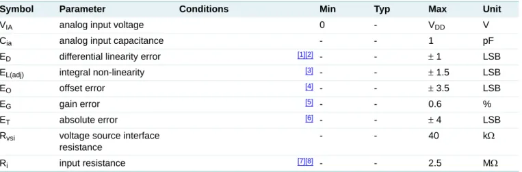
Fig 1. LPC11Cx2/Cx4 block diagram
SRAM 8 kB ARM CORTEX-M0 TEST/DEBUG INTERFACE FLASH 16/32 kB HIGH-SPEED GPIO AHB TO APB BRIDGE CLOCK GENERATION, POWER CONTROL, SYSTEM FUNCTIONS XTALIN XTALOUT RESET clocks and controls SWD LPC11Cx2/Cx4 002aaf265 slave slave slave slave ROM slave AHB-LITE BUS GPIO ports PIO0/1/2/3 CLKOUT IRC POR SPI0 10-bit ADC UART 32-bit COUNTER/TIMER 0 I2C-BUS WDT IOCONFIG CT32B0_MAT[3:0] AD[7:0] CT32B0_CAP0 SDA SCL RXD TXD DTR, DSR, CTS, DCD, RI, RTS SYSTEM CONTROL PMU 32-bit COUNTER/TIMER 1 CT32B1_MAT[3:0] CT32B1_CAP0 16-bit COUNTER/TIMER 1 CT16B1_MAT[1:0](1) CT16B1_CAP0 C_CAN (LPC11C12/C14) CAN_TXD CAN_RXD C_CAN/ ON-CHIP TRANSCEIVER (LPC11C22/C24) CANL, CANH STB VCC, VDD_CAN 16-bit COUNTER/TIMER 0 CT16B0_MAT[2:0] CT16B0_CAP0 SCK0, SSEL0 MISO0, MOSI0 SCK1, SSEL1 MISO1, MOSI1 SPI1 system bus
6. Pinning
information
6.1 Pinning
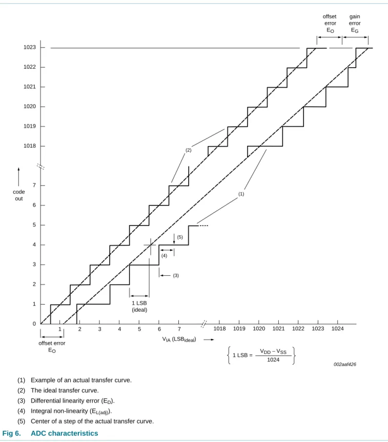
Fig 2. Pin configuration (LPC11C12/C14)
LPC11C12FBD48/301 LPC11C14FBD48/301 PIO2_6 PIO3_0/DTR PIO2_0/DTR/SSEL1 R/PIO1_2/AD3/CT32B1_MAT1 RESET/PIO0_0 R/PIO1_1/AD2/CT32B1_MAT0 PIO0_1/CLKOUT/CT32B0_MAT2 R/PIO1_0/AD1/CT32B1_CAP0 VSS R/PIO0_11/AD0/CT32B0_MAT3 XTALIN PIO2_11/SCK0 XTALOUT PIO1_10/AD6/CT16B1_MAT1 VDD SWCLK/PIO0_10/SCK0/CT16B0_MAT2 PIO1_8/CT16B1_CAP0 PIO0_9/MOSI0/CT16B0_MAT1 PIO0_2/SSEL0/CT16B0_CAP0 PIO0_8/MISO0/CT16B0_MAT0 PIO2_7 PIO2_2/DCD/MISO1 PIO2_8 PIO2_10 PIO2_1/DSR/SCK1 PIO3_3/RI PIO0_3 PIO1_7/TXD/CT32B0_MAT1 PIO0_4/SCL PIO1_6/RXD/CT32B0_MAT0 PIO0_5/SDA PIO1_5/RTS/CT32B0_CAP0 PIO1_9/CT16B1_MAT0 VDD PIO2_4 PIO3_2/DCD CAN_RXD PIO1_11/AD7 CAN_TXD VSS PIO2_5 PIO1_4/AD5/CT32B1_MAT3/WAKEUP PIO0_6/SCK0 SWDIO/PIO1_3/AD4/CT32B1_MAT2 PIO0_7/CTS PIO2_9 PIO2_3/RI/MOSI1 PIO3_1/DSR 002aaf266 1 2 3 4 5 6 7 8 9 10 11 12 36 35 34 33 32 31 30 29 28 27 26 25 13 14 15 16 17 18 19 20 21 22 23 48 47 46 45 44 43 42 41 40 39 38 37 24
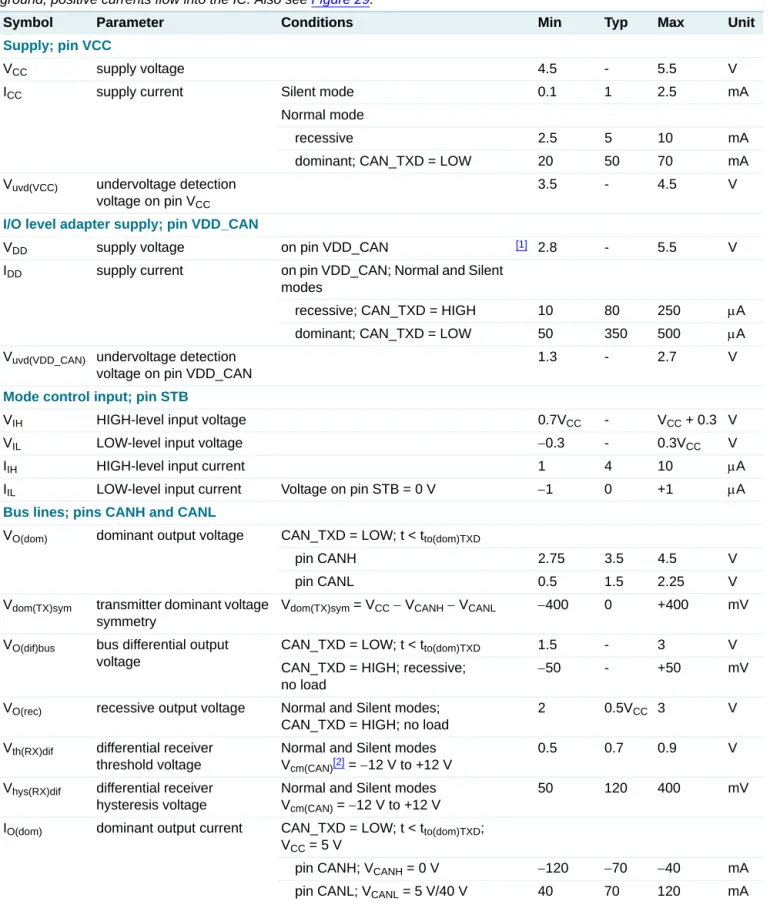
Fig 3. Pin configuration (LPC11C22/C24) LPC11C22FBD48/301 LPC11C24FBD48/301 PIO2_6 PIO3_0/DTR PIO2_0/DTR/SSEL1 R/PIO1_2/AD3/CT32B1_MAT1 RESET/PIO0_0 R/PIO1_1/AD2/CT32B1_MAT0 PIO0_1/CLKOUT/CT32B0_MAT2 R/PIO1_0/AD1/CT32B1_CAP0 VSS R/PIO0_11/AD0/CT32B0_MAT3 XTALIN PIO2_11/SCK0 XTALOUT PIO1_10/AD6/CT16B1_MAT1 VDD SWCLK/PIO0_10/SCK0/CT16B0_MAT2 PIO1_8/CT16B1_CAP0 PIO0_9/MOSI0/CT16B0_MAT1 PIO0_2/SSEL0/CT16B0_CAP0 PIO0_8/MISO0/CT16B0_MAT0 PIO2_7 PIO2_2/DCD/MISO1 PIO2_8 PIO2_10 PIO2_1/DSR/SCK1 PIO3_3/RI PIO0_3 PIO1_7/TXD/CT32B0_MAT1 PIO0_4/SCL PIO1_6/RXD/CT32B0_MAT0 PIO0_5/SDA PIO1_5/RTS/CT32B0_CAP0 VDD_CAN VDD CANL PIO3_2/DCD CANH PIO1_11/AD7 VCC VSS GND PIO1_4/AD5/CT32B1_MAT3/WAKEUP STB SWDIO/PIO1_3/AD4/CT32B1_MAT2 PIO0_6/SCK0 PIO0_7/CTS PIO2_3/RI/MOSI1 PIO3_1/DSR 002aaf909 1 2 3 4 5 6 7 8 9 10 11 12 36 35 34 33 32 31 30 29 28 27 26 25 13 14 15 16 17 18 19 20 21 22 23 48 47 46 45 44 43 42 41 40 39 38 37 24
6.2 Pin description
Table 3. LPC11C12/C14 pin description table
Symbol Pin Start logic inputs Type Reset state [1] Description
PIO0_0 to PIO0_11 Port 0 — Port 0 is a 12-bit I/O port with individual direction and
function controls for each bit. The operation of port 0 pins depends on the function selected through the IOCONFIG register block.
RESET/PIO0_0 3[2] yes I I; PU RESET — External reset input with 20 ns glitch filter. A LOW-going
pulse as short as 50 ns on this pin resets the device, causing I/O ports and peripherals to take on their default states, and processor execution to begin at address 0.
I/O - PIO0_0 — General purpose digital input/output pin with 10 ns glitch filter.
PIO0_1/CLKOUT/ CT32B0_MAT2
4[3] yes I/O I; PU PIO0_1 — General purpose digital input/output pin. A LOW level on
this pin during reset starts the flash ISP command handler via UART (if PIO0_3 is HIGH) or via C_CAN (if PIO0_3 is LOW).
O - CLKOUT — Clockout pin.
O - CT32B0_MAT2 — Match output 2 for 32-bit timer 0. PIO0_2/SSEL0/
CT16B0_CAP0
10[3] yes I/O I; PU PIO0_2 — General purpose digital input/output pin.
I/O - SSEL0 — Slave Select for SPI0.
I - CT16B0_CAP0 — Capture input 0 for 16-bit timer 0.
PIO0_3 14[3] yes I/O I; PU PIO0_3 — General purpose digital input/output pin. This pin is
monitored during reset: Together with a LOW level on pin PIO0_1, a LOW level starts the flash ISP command handler via C_CAN and a HIGH level starts the flash ISP command handler via UART.
PIO0_4/SCL 15[4] yes I/O I; IA PIO0_4 — General purpose digital input/output pin (open-drain).
I/O - SCL — I2C-bus, open-drain clock input/output. High-current sink only
if I2C Fast-mode Plus is selected in the I/O configuration register.
PIO0_5/SDA 16[4] yes I/O I; IA PIO0_5 — General purpose digital input/output pin (open-drain).
I/O - SDA — I2C-bus, open-drain data input/output. High-current sink only
if I2C Fast-mode Plus is selected in the I/O configuration register.
PIO0_6/SCK0 22[3] yes I/O I; PU PIO0_6 — General purpose digital input/output pin.
I/O - SCK0 — Serial clock for SPI0.
PIO0_7/CTS 23[3] yes I/O I; PU PIO0_7 — General purpose digital input/output pin (high-current
output driver).
I - CTS — Clear To Send input for UART. PIO0_8/MISO0/
CT16B0_MAT0
27[3] yes I/O I; PU PIO0_8 — General purpose digital input/output pin.
I/O - MISO0 — Master In Slave Out for SPI0.
O - CT16B0_MAT0 — Match output 0 for 16-bit timer 0. PIO0_9/MOSI0/
CT16B0_MAT1
28[3] yes I/O I; PU PIO0_9 — General purpose digital input/output pin.
I/O - MOSI0 — Master Out Slave In for SPI0.
O - CT16B0_MAT1 — Match output 1 for 16-bit timer 0. SWCLK/PIO0_10/
SCK0/
CT16B0_MAT2
29[3] yes I I; PU SWCLK — Serial wire clock.
I/O - PIO0_10 — General purpose digital input/output pin. I/O - SCK0 — Serial clock for SPI0.
R/PIO0_11/ AD0/
CT32B0_MAT3
32[5] yes - I; PU R — Reserved. Configure for an alternate function in the IOCONFIG
block.
I/O - PIO0_11 — General purpose digital input/output pin. I - AD0 — A/D converter, input 0.
O - CT32B0_MAT3 — Match output 3 for 32-bit timer 0.
PIO1_0 to PIO1_11 Port 1 — Port 1 is a 12-bit I/O port with individual direction and
function controls for each bit. The operation of port 1 pins depends on the function selected through the IOCONFIG register block. R/PIO1_0/AD1/
CT32B1_CAP0
33[5] yes - I; PU R — Reserved. Configure for an alternate function in the IOCONFIG
block.
I/O - PIO1_0 — General purpose digital input/output pin. I - AD1 — A/D converter, input 1.
I - CT32B1_CAP0 — Capture input 0 for 32-bit timer 1. R/PIO1_1/AD2/
CT32B1_MAT0
34[5] no - I; PU R — Reserved. Configure for an alternate function in the IOCONFIG
block.
I/O - PIO1_1 — General purpose digital input/output pin. I - AD2 — A/D converter, input 2.
O - CT32B1_MAT0 — Match output 0 for 32-bit timer 1. R/PIO1_2/AD3/
CT32B1_MAT1
35[5] no - I; PU R — Reserved. Configure for an alternate function in the IOCONFIG
block.
I/O - PIO1_2 — General purpose digital input/output pin. I - AD3 — A/D converter, input 3.
O - CT32B1_MAT1 — Match output 1 for 32-bit timer 1. SWDIO/PIO1_3/
AD4/
CT32B1_MAT2
39[5] no I/O I; PU SWDIO — Serial wire debug input/output.
I/O - PIO1_3 — General purpose digital input/output pin. I - AD4 — A/D converter, input 4.
O - CT32B1_MAT2 — Match output 2 for 32-bit timer 1. PIO1_4/AD5/
CT32B1_MAT3/ WAKEUP
40[5] no I/O I; PU PIO1_4 — General purpose digital input/output pin with 10 ns glitch
filter.
I - AD5 — A/D converter, input 5.
O - CT32B1_MAT3 — Match output 3 for 32-bit timer 1.
I - WAKEUP — Deep power-down mode wake-up pin with 20 ns glitch filter. This pin must be pulled HIGH externally to enter Deep power-down mode and pulled LOW to exit Deep power-down mode. A LOW-going pulse as short as 50 ns wakes up the part.
PIO1_5/RTS/ CT32B0_CAP0
45[3] no I/O I; PU PIO1_5 — General purpose digital input/output pin.
O - RTS — Request To Send output for UART.
I - CT32B0_CAP0 — Capture input 0 for 32-bit timer 0. PIO1_6/RXD/
CT32B0_MAT0
46[3] no I/O I; PU PIO1_6 — General purpose digital input/output pin.
I - RXD — Receiver input for UART.
O - CT32B0_MAT0 — Match output 0 for 32-bit timer 0.
Table 3. LPC11C12/C14 pin description table
Symbol Pin Start logic inputs Type Reset state [1] Description
PIO1_7/TXD/ CT32B0_MAT1
47[3] no I/O I; PU PIO1_7 — General purpose digital input/output pin.
O - TXD — Transmitter output for UART.
O - CT32B0_MAT1 — Match output 1 for 32-bit timer 0. PIO1_8/
CT16B1_CAP0
9[3] no I/O I; PU PIO1_8 — General purpose digital input/output pin.
I - CT16B1_CAP0 — Capture input 0 for 16-bit timer 1. PIO1_9/
CT16B1_MAT0
17[3] no I/O I; PU PIO1_9 — General purpose digital input/output pin.
O - CT16B1_MAT0 — Match output 0 for 16-bit timer 1. PIO1_10/AD6/
CT16B1_MAT1
30[5] no I/O I; PU PIO1_10 — General purpose digital input/output pin.
I - AD6 — A/D converter, input 6.
O - CT16B1_MAT1 — Match output 1 for 16-bit timer 1.
PIO1_11/AD7 42[5] no I/O I; PU PIO1_11 — General purpose digital input/output pin.
I - AD7 — A/D converter, input 7.
PIO2_0 to PIO2_11 Port 2 — Port 2 is a 12-bit I/O port with individual direction and
function controls for each bit. The operation of port 2 pins depends on the function selected through the IOCONFIG register block. PIO2_0/DTR/
SSEL1
2[3] no I/O I; PU PIO2_0 — General purpose digital input/output pin.
I/O - DTR — Data Terminal Ready output for UART. I/O - SSEL1 — Slave Select for SPI1.
PIO2_1/DSR/SCK1 13[3] no I/O I; PU PIO2_1 — General purpose digital input/output pin.
I - DSR — Data Set Ready input for UART. I/O - SCK1 — Serial clock for SPI1.
PIO2_2/DCD/ MISO1
26[3] no I/O I; PU PIO2_2 — General purpose digital input/output pin.
I - DCD — Data Carrier Detect input for UART. I/O - MISO1 — Master In Slave Out for SPI1.
PIO2_3/RI/MOSI1 38[3] no I/O I; PU PIO2_3 — General purpose digital input/output pin.
I - RI — Ring Indicator input for UART. I/O - MOSI1 — Master Out Slave In for SPI1.
PIO2_4 18[3] no I/O I; PU PIO2_4 — General purpose digital input/output pin.
PIO2_5 21[3] no I/O I; PU PIO2_5 — General purpose digital input/output pin.
PIO2_6 1[3] no I/O I; PU PIO2_6 — General purpose digital input/output pin.
PIO2_7 11[3] no I/O I; PU PIO2_7 — General purpose digital input/output pin.
PIO2_8 12[3] no I/O I; PU PIO2_8 — General purpose digital input/output pin.
PIO2_9 24[3] no I/O I; PU PIO2_9 — General purpose digital input/output pin.
PIO2_10 25[3] no I/O I; PU PIO2_10 — General purpose digital input/output pin.
PIO2_11/SCK0 31[3] no I/O I; PU PIO2_11 — General purpose digital input/output pin.
I/O - SCK0 — Serial clock for SPI0.
PIO3_0 to PIO3_3 Port 3 — Port 3 is a 12-bit I/O port with individual direction and
function controls for each bit. The operation of port 3 pins depends on the function selected through the IOCONFIG register block. Pins PIO3_4 to PIO3_11 are not available.
Table 3. LPC11C12/C14 pin description table
Symbol Pin Start logic inputs Type Reset state [1] Description
[1] Pin state at reset for default function: I = Input; O = Output; PU = internal pull-up enabled (pins pulled up to full VDD level); IA = inactive, no pull-up/down enabled.
[2] 5 V tolerant pad. RESET functionality is not available in Deep power-down mode. Use the WAKEUP pin to reset the chip and wake up from Deep power-down mode. An external pull-up resistor is required on this pin for the Deep power-down mode. See Figure 27 for the reset pad configuration.
[3] 5 V tolerant pad providing digital I/O functions with configurable pull-up/pull-down resistors and configurable hysteresis (see Figure 26). [4] I2C-bus pads compliant with the I2C-bus specification for I2C standard mode and I2C Fast-mode Plus.
[5] 5 V tolerant pad providing digital I/O functions with configurable pull-up/pull-down resistors, configurable hysteresis, and analog input. When configured as a ADC input, digital section of the pad is disabled and the pin is not 5 V tolerant (see Figure 26).
[6] 5 V tolerant digital I/O pad without pull-up/pull-down resistors.
[7] When the system oscillator is not used, connect XTALIN and XTALOUT as follows: XTALIN can be left floating or can be grounded (grounding is preferred to reduce susceptibility to noise). XTALOUT should be left floating.
PIO3_0/DTR 36[3] no I/O I; PU PIO3_0 — General purpose digital input/output pin.
O - DTR — Data Terminal Ready output for UART.
PIO3_1/DSR 37[3] no I/O I; PU PIO3_1 — General purpose digital input/output pin.
I - DSR — Data Set Ready input for UART.
PIO3_2/DCD 43[3] no I/O I; PU PIO3_2 — General purpose digital input/output pin.
I DCD — Data Carrier Detect input for UART.
PIO3_3/RI 48[3] no I/O I; PU PIO3_3 — General purpose digital input/output pin.
I - RI — Ring Indicator input for UART.
CAN_RXD 19[6] no I I; IA CAN_RXD — C_CAN receive data input.
CAN_TXD 20[6] no O I; IA CAN_TXD — C_CAN transmit data output.
VDD 8; 44 - I - Supply voltage to the internal regulator, the external rail, and the
ADC. Also used as the ADC reference voltage.
XTALIN 6[7] - I - Input to the oscillator circuit and internal clock generator circuits.
Input voltage must not exceed 1.8 V.
XTALOUT 7[7] - O - Output from the oscillator amplifier.
VSS 5; 41 - I - Ground.
Table 3. LPC11C12/C14 pin description table
Symbol Pin Start logic inputs Type Reset state [1] Description
Table 4. LPC11C22/C24 pin description table
Symbol Pin Start logic inputs Type Reset state [1] Description
PIO0_0 to PIO0_11 Port 0 — Port 0 is a 12-bit I/O port with individual direction and
function controls for each bit. The operation of port 0 pins depends on the function selected through the IOCONFIG register block.
RESET/PIO0_0 3[2] yes I I; PU RESET — External reset input with 20 ns glitch filter. A LOW-going
pulse as short as 50 ns on this pin resets the device, causing I/O ports and peripherals to take on their default states, and processor execution to begin at address 0.
I/O - PIO0_0 — General purpose digital input/output pin with 10 ns glitch filter.
PIO0_1/CLKOUT/ CT32B0_MAT2
4[3] yes I/O I; PU PIO0_1 — General purpose digital input/output pin. A LOW level on
this pin during reset starts the flash ISP command handler via UART (if PIO0_3 is HIGH) or via C_CAN (if PIO0_3 is LOW).
O - CLKOUT — Clockout pin.
O - CT32B0_MAT2 — Match output 2 for 32-bit timer 0. PIO0_2/SSEL0/
CT16B0_CAP0
10[3] yes I/O I; PU PIO0_2 — General purpose digital input/output pin.
I/O - SSEL0 — Slave Select for SPI0.
I - CT16B0_CAP0 — Capture input 0 for 16-bit timer 0.
PIO0_3 14[3] yes I/O I; PU PIO0_3 — General purpose digital input/output pin. This pin is
monitored during reset: Together with a LOW level on pin PIO0_1, a LOW level starts the flash ISP command handler via C_CAN and a HIGH level starts the flash ISP command handler via UART.
PIO0_4/SCL 15[4] yes I/O I; IA PIO0_4 — General purpose digital input/output pin (open-drain).
I/O - SCL — I2C-bus, open-drain clock input/output. High-current sink only
if I2C Fast-mode Plus is selected in the I/O configuration register.
PIO0_5/SDA 16[4] yes I/O I; IA PIO0_5 — General purpose digital input/output pin (open-drain).
I/O - SDA — I2C-bus, open-drain data input/output. High-current sink only
if I2C Fast-mode Plus is selected in the I/O configuration register.
PIO0_6/SCK0 23[3] yes I/O I; PU PIO0_6 — General purpose digital input/output pin.
I/O - SCK0 — Serial clock for SPI0.
PIO0_7/CTS 24[3] yes I/O I; PU PIO0_7 — General purpose digital input/output pin (high-current
output driver).
I - CTS — Clear To Send input for UART. PIO0_8/MISO0/
CT16B0_MAT0
27[3] yes I/O I; PU PIO0_8 — General purpose digital input/output pin.
I/O - MISO0 — Master In Slave Out for SPI0.
O - CT16B0_MAT0 — Match output 0 for 16-bit timer 0. PIO0_9/MOSI0/
CT16B0_MAT1
28[3] yes I/O I; PU PIO0_9 — General purpose digital input/output pin.
I/O - MOSI0 — Master Out Slave In for SPI0.
O - CT16B0_MAT1 — Match output 1 for 16-bit timer 0. SWCLK/PIO0_10/
SCK0/
CT16B0_MAT2
29[3] yes I I; PU SWCLK — Serial wire clock.
I/O - PIO0_10 — General purpose digital input/output pin. I/O - SCK0 — Serial clock for SPI0.
O - CT16B0_MAT2 — Match output 2 for 16-bit timer 0. R/PIO0_11/
AD0/
CT32B0_MAT3
32[5] yes - I; PU R — Reserved. Configure for an alternate function in the IOCONFIG
block.
I/O - PIO0_11 — General purpose digital input/output pin. I - AD0 — A/D converter, input 0.
O - CT32B0_MAT3 — Match output 3 for 32-bit timer 0.
PIO1_0 to PIO1_11 Port 1 — Port 1 is a 12-bit I/O port with individual direction and
function controls for each bit. The operation of port 1 pins depends on the function selected through the IOCONFIG register block.
Table 4. LPC11C22/C24 pin description table
Symbol Pin Start logic inputs Type Reset state [1] Description
R/PIO1_0/AD1/ CT32B1_CAP0
33[5] yes - I; PU R — Reserved. Configure for an alternate function in the IOCONFIG
block.
I/O - PIO1_0 — General purpose digital input/output pin. I - AD1 — A/D converter, input 1.
I - CT32B1_CAP0 — Capture input 0 for 32-bit timer 1. R/PIO1_1/AD2/
CT32B1_MAT0
34[5] no - I; PU R — Reserved. Configure for an alternate function in the IOCONFIG
block.
I/O - PIO1_1 — General purpose digital input/output pin. I - AD2 — A/D converter, input 2.
O - CT32B1_MAT0 — Match output 0 for 32-bit timer 1. R/PIO1_2/AD3/
CT32B1_MAT1
35[5] no - I; PU R — Reserved. Configure for an alternate function in the IOCONFIG
block.
I/O - PIO1_2 — General purpose digital input/output pin. I - AD3 — A/D converter, input 3.
O - CT32B1_MAT1 — Match output 1 for 32-bit timer 1. SWDIO/PIO1_3/
AD4/
CT32B1_MAT2
39[5] no I/O I; PU SWDIO — Serial wire debug input/output.
I/O - PIO1_3 — General purpose digital input/output pin. I - AD4 — A/D converter, input 4.
O - CT32B1_MAT2 — Match output 2 for 32-bit timer 1. PIO1_4/AD5/
CT32B1_MAT3/ WAKEUP
40[5] no I/O I; PU PIO1_4 — General purpose digital input/output pin with 10 ns glitch
filter.
I - AD5 — A/D converter, input 5.
O - CT32B1_MAT3 — Match output 3 for 32-bit timer 1.
I - WAKEUP — Deep power-down mode wake-up pin with 20 ns glitch filter. This pin must be pulled HIGH externally to enter Deep power-down mode and pulled LOW to exit Deep power-down mode. A LOW-going pulse as short as 50 ns wakes up the part.
PIO1_5/RTS/ CT32B0_CAP0
45[3] no I/O I; PU PIO1_5 — General purpose digital input/output pin.
O - RTS — Request To Send output for UART.
I - CT32B0_CAP0 — Capture input 0 for 32-bit timer 0. PIO1_6/RXD/
CT32B0_MAT0
46[3] no I/O I; PU PIO1_6 — General purpose digital input/output pin.
I - RXD — Receiver input for UART.
O - CT32B0_MAT0 — Match output 0 for 32-bit timer 0. PIO1_7/TXD/
CT32B0_MAT1
47[3] no I/O I; PU PIO1_7 — General purpose digital input/output pin.
O - TXD — Transmitter output for UART.
O - CT32B0_MAT1 — Match output 1 for 32-bit timer 0. PIO1_8/
CT16B1_CAP0
9[3] no I/O I; PU PIO1_8 — General purpose digital input/output pin.
I - CT16B1_CAP0 — Capture input 0 for 16-bit timer 1. PIO1_10/AD6/
CT16B1_MAT1
30[5] no I/O I; PU PIO1_10 — General purpose digital input/output pin.
I - AD6 — A/D converter, input 6.
O - CT16B1_MAT1 — Match output 1 for 16-bit timer 1.
Table 4. LPC11C22/C24 pin description table
Symbol Pin Start logic inputs Type Reset state [1] Description
PIO1_11/AD7 42[5] no I/O I; PU PIO1_11 — General purpose digital input/output pin. I - AD7 — A/D converter, input 7.
PIO2_0 to PIO2_11 Port 2 — Port 2 is a 12-bit I/O port with individual direction and
function controls for each bit. The operation of port 2 pins depends on the function selected through the IOCONFIG register block. PIO2_0/DTR/
SSEL1
2[3] no I/O I; PU PIO2_0 — General purpose digital input/output pin.
I/O - DTR — Data Terminal Ready output for UART. I/O - SSEL1 — Slave Select for SPI1.
PIO2_1/DSR/SCK1 13[3] no I/O I; PU PIO2_1 — General purpose digital input/output pin.
I - DSR — Data Set Ready input for UART. I/O - SCK1 — Serial clock for SPI1.
PIO2_2/DCD/ MISO1
26[3] no I/O I; PU PIO2_2 — General purpose digital input/output pin.
I - DCD — Data Carrier Detect input for UART. I/O - MISO1 — Master In Slave Out for SPI1.
PIO2_3/RI/MOSI1 38[3] no I/O I; PU PIO2_3 — General purpose digital input/output pin.
I - RI — Ring Indicator input for UART. I/O - MOSI1 — Master Out Slave In for SPI1.
PIO2_6 1[3] no I/O I; PU PIO2_6 — General purpose digital input/output pin.
PIO2_7 11[3] no I/O I; PU PIO2_7 — General purpose digital input/output pin.
PIO2_8 12[3] no I/O I; PU PIO2_8 — General purpose digital input/output pin.
PIO2_10 25[3] no I/O I; PU PIO2_10 — General purpose digital input/output pin.
PIO2_11/SCK0 31[3] no I/O I; PU PIO2_11 — General purpose digital input/output pin.
I/O - SCK0 — Serial clock for SPI0.
PIO3_0 to PIO3_3 Port 3 — Port 3 is a 12-bit I/O port with individual direction and
function controls for each bit. The operation of port 3 pins depends on the function selected through the IOCONFIG register block. Pins PIO3_4 to PIO3_11 are not available.
PIO3_0/DTR 36[3] no I/O I; PU PIO3_0 — General purpose digital input/output pin.
O - DTR — Data Terminal Ready output for UART.
PIO3_1/DSR 37[3] no I/O I; PU PIO3_1 — General purpose digital input/output pin.
I - DSR — Data Set Ready input for UART.
PIO3_2/DCD 43[3] no I/O I; PU PIO3_2 — General purpose digital input/output pin.
I DCD — Data Carrier Detect input for UART.
PIO3_3/RI 48[3] no I/O I; PU PIO3_3 — General purpose digital input/output pin.
I - RI — Ring Indicator input for UART.
CANL 18 no I/O - LOW-level CAN bus line.
CANH 19 no I/O - HIGH-level CAN bus line.
STB 22 no I - Silent mode control input for CAN transceiver (LOW = Normal mode,
HIGH = silent mode).
VDD_CAN 17 - - - Supply voltage for I/O level of CAN transceiver.
VCC 20 - - - Supply voltage for CAN transceiver.
Table 4. LPC11C22/C24 pin description table
Symbol Pin Start logic inputs Type Reset state [1] Description
[1] Pin state at reset for default function: I = Input; O = Output; PU = internal pull-up enabled (pins pulled up to full VDD level); IA = inactive, no pull-up/down enabled.
[2] 5 V tolerant pad. RESET functionality is not available in Deep power-down mode. Use the WAKEUP pin to reset the chip and wake up from Deep power-down mode. An external pull-up resistor is required on this pin for the Deep power-down mode. See Figure 27 for the reset pad configuration.
[3] 5 V tolerant pad providing digital I/O functions with configurable pull-up/pull-down resistors and configurable hysteresis (see Figure 26). [4] I2C-bus pads compliant with the I2C-bus specification for I2C standard mode and I2C Fast-mode Plus.
[5] 5 V tolerant pad providing digital I/O functions with configurable pull-up/pull-down resistors, configurable hysteresis, and analog input. When configured as a ADC input, digital section of the pad is disabled and the pin is not 5 V tolerant (see Figure 26).
[6] 5 V tolerant digital I/O pad without pull-up/pull-down resistors.
[7] When the system oscillator is not used, connect XTALIN and XTALOUT as follows: XTALIN can be left floating or can be grounded (grounding is preferred to reduce susceptibility to noise). XTALOUT should be left floating.
GND 21 - - - Ground for CAN transceiver.
VDD 8; 44 - I - Supply voltage to the internal regulator, the external rail, and the
ADC. Also used as the ADC reference voltage.
XTALIN 6[7] - I - Input to the oscillator circuit and internal clock generator circuits.
Input voltage must not exceed 1.8 V.
XTALOUT 7[7] - O - Output from the oscillator amplifier.
VSS 5; 41 - I - Ground.
Table 4. LPC11C22/C24 pin description table
Symbol Pin Start logic inputs Type Reset state [1] Description
7. Functional
description
7.1 ARM Cortex-M0 processor
The ARM Cortex-M0 is a general purpose, 32-bit microprocessor, which offers high performance and very low power consumption.
7.2 On-chip flash program memory
The LPC11Cx2/Cx4 contain 32 kB (LPC11C14/C24) or 16 kB (LPC11C12/C22) of on-chip flash program memory.
7.3 On-chip SRAM
The LPC11Cx2/Cx4 contain a total of 8 kB on-chip static RAM data memory.
7.4 Memory map
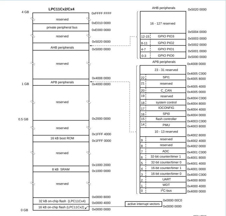
The LPC11Cx2/Cx4 incorporates several distinct memory regions, shown in the following figures. Figure 4 shows the overall map of the entire address space from the user program viewpoint following reset. The interrupt vector area supports address remapping. The AHB peripheral area is 2 megabyte in size, and is divided to allow for up to 128 peripherals. The APB peripheral area is 512 kB in size and is divided to allow for up to 32 peripherals. Each peripheral of either type is allocated 16 kilobytes of space. This allows simplifying the address decoding for each peripheral.
7.5 Nested Vectored Interrupt Controller (NVIC)
The Nested Vectored Interrupt Controller (NVIC) is an integral part of the Cortex-M0. The tight coupling to the CPU allows for low interrupt latency and efficient processing of late arriving interrupts.
7.5.1 Features
•
Controls system exceptions and peripheral interrupts.•
In the LPC11Cx2/Cx4, the NVIC supports 32 vectored interrupts including 13 inputs to the start logic from individual GPIO pins.Fig 4. LPC11Cx2/Cx4 memory map
0x5000 0000 0x5001 0000 0x5002 0000 0x5020 0000 AHB peripherals 16 - 127 reserved GPIO PIO1 4-7 0x5003 0000 0x5004 0000 GPIO PIO2 GPIO PIO3 8-11 12-15 GPIO PIO0 0-3 APB peripherals 0x4000 4000 0x4000 8000 0x4000 C000 0x4001 0000 0x4001 8000 0x4002 0000 0x4002 8000 0x4003 8000 0x4003 C000 0x4004 0000 0x4004 4000 0x4004 8000 0x4004 C000 0x4005 0000 0x4005 4000 0x4005 8000 0x4005 C000 0x4008 0000 0x4002 4000 0x4001 C000 0x4001 4000 0x4000 0000 WDT 32-bit counter/timer 0 32-bit counter/timer 1 ADC UART PMU I2C-bus 10 - 13 reserved reserved reserved reserved 23 - 31 reserved 0 1 2 3 4 5 6 7 8 9 16 15 14 17 18 reserved reserved reserved 0x0000 0000 0 GB 0.5 GB 4 GB 1 GB 0x1000 2000 0x1FFF 0000 0x1FFF 4000 0x2000 0000 0x4000 0000 0x4008 0000 0x5000 0000 0x5020 0000 0xFFFF FFFF reserved reserved reserved APB peripherals AHB peripherals 0x1000 0000 8 kB SRAM LPC11Cx2/Cx4 0x0000 4000 16 kB on-chip flash (LPC11Cx2) 0x0000 8000 32 kB on-chip flash (LPC11Cx4) 16 kB boot ROM 0x0000 0000 0x0000 00C0 active interrupt vectors
002aaf268 reserved SPI0 16-bit counter/timer 1 16-bit counter/timer 0 IOCONFIG system control 20 19 C_CAN reserved 22 21 SPI1 flash controller 0xE000 0000 0xE010 0000 private peripheral bus
•
Four programmable interrupt priority levels, with hardware priority level masking.•
Software interrupt generation.7.5.2 Interrupt sources
Each peripheral device has one interrupt line connected to the NVIC but may have several interrupt flags. Individual interrupt flags may also represent more than one interrupt source.
Any GPIO pin (total of 40 pins (LPC11C12/C14) or 36 pins (LPC11C22/C24)) regardless of the selected function, can be programmed to generate an interrupt on a level, or rising edge or falling edge, or both.
7.6 IOCONFIG block
The IOCONFIG block allows selected pins of the microcontroller to have more than one function. Configuration registers control the multiplexers to allow connection between the pin and the on-chip peripherals.
Peripherals should be connected to the appropriate pins prior to being activated and prior to any related interrupt(s) being enabled. Activity of any enabled peripheral function that is not mapped to a related pin should be considered undefined.
7.7 Fast general purpose parallel I/O
Device pins that are not connected to a specific peripheral function are controlled by the GPIO registers. Pins may be dynamically configured as inputs or outputs. Multiple outputs can be set or cleared in one write operation.
LPC11Cx2/Cx4 use accelerated GPIO functions:
•
GPIO registers are a dedicated AHB peripheral so that the fastest possible I/O timing can be achieved.•
Entire port value can be written in one instruction.Additionally, any GPIO pin (total of 40 pins (LPC11C12/C14) or 36 pins (LPC11C22/C24)) providing a digital function can be programmed to generate an interrupt on a level, a rising or falling edge, or both.
7.7.1 Features
•
Bit level port registers allow a single instruction to set or clear any number of bits in one write operation.•
Direction control of individual bits.•
All GPIO pins default to inputs with pull-ups enabled after reset except for the I2C-bus true open-drain pins PIO0_4 and PIO0_5.•
Pull-up/pull-down resistor configuration can be programmed through the IOCONFIG block for each GPIO pin (except PIO0_4 and PIO0_5).•
All GPIO pins (except PIO0_4 and PIO0_5) are pulled up to 3.3 V (VDD = 3.3 V) if their pull-up resistor is enabled in the IOCONFIG block.7.8 UART
The LPC11Cx2/Cx4 contain one UART.
Support for RS-485/9-bit mode allows both software address detection and automatic address detection using 9-bit mode.
The UART includes a fractional baud rate generator. Standard baud rates such as 115200 Bd can be achieved with any crystal frequency above 2 MHz.
7.8.1 Features
•
Maximum UART data bit rate of 3.125 Mbit/s.•
16 Byte Receive and Transmit FIFOs.•
Register locations conform to 16C550 industry standard.•
Receiver FIFO trigger points at 1 B, 4 B, 8 B, and 14 B.•
Built-in fractional baud rate generator covering wide range of baud rates without a need for external crystals of particular values.•
FIFO control mechanism that enables software flow control implementation.•
Support for RS-485/9-bit mode.•
Support for modem control.7.9 SPI serial I/O controller
The LPC11Cx2/Cx4 contain two SPI controllers. Both SPI controllers support SSP features.
The SPI controller is capable of operation on a SSP, 4-wire SSI, or Microwire bus. It can interact with multiple masters and slaves on the bus. Only a single master and a single slave can communicate on the bus during a given data transfer. The SPI supports full duplex transfers, with frames of 4 bits to 16 bits of data flowing from the master to the slave and from the slave to the master. In practice, often only one of these data flows carries meaningful data.
7.9.1 Features
•
Maximum SPI speed of 25 Mbit/s (master) or 4.17 Mbit/s (slave) (in SSP mode)•
Compatible with Motorola SPI, 4-wire Texas Instruments SSI, and NationalSemiconductor Microwire buses
•
Synchronous serial communication•
Master or slave operation•
8-frame FIFOs for both transmit and receive•
4-bit to 16-bit frame7.10 I
2C-bus serial I/O controller
The I2C-bus is bidirectional for inter-IC control using only two wires: a Serial CLock line (SCL) and a Serial DAta line (SDA). Each device is recognized by a unique address and can operate as either a receiver-only device (e.g., an LCD driver) or a transmitter with the capability to both receive and send information (such as memory). Transmitters and/or receivers can operate in either master or slave mode, depending on whether the chip has to initiate a data transfer or is only addressed. The I2C is a multi-master bus and can be controlled by more than one bus master connected to it.
7.10.1 Features
•
The I2C-interface is a standard I2C-bus compliant interface with open-drain pins. The I2C-bus interface also supports Fast-mode Plus with bit rates up to 1 Mbit/s.•
Easy to configure as master, slave, or master/slave.•
Programmable clocks allow versatile rate control.•
Bidirectional data transfer between masters and slaves.•
Multi-master bus (no central master).•
Arbitration between simultaneously transmitting masters without corruption of serial data on the bus.•
Serial clock synchronization allows devices with different bit rates to communicate via one serial bus.•
Serial clock synchronization can be used as a handshake mechanism to suspend and resume serial transfer.•
The I2C-bus can be used for test and diagnostic purposes.•
The I2C-bus controller supports multiple address recognition and a bus monitor mode.7.11 C_CAN controller
Controller Area Network (CAN) is the definition of a high performance communication protocol for serial data communication. The C_CAN controller is designed to provide a full implementation of the CAN protocol according to the CAN Specification Version 2.0B. The C_CAN controller allows to build powerful local networks with low-cost multiplex wiring by supporting distributed real-time control with a very high level of security.
On-chip C_CAN drivers provide an API for initialization and communication using CAN and CANopen standards.
7.11.1 Features
•
Conforms to protocol version 2.0 parts A and B.•
Supports bit rate of up to 1 Mbit/s.•
Supports 32 Message Objects.•
Each Message Object has its own identifier mask.•
Provides programmable FIFO mode (concatenation of Message Objects).•
Provides maskable interrupts.•
Supports Disabled Automatic Retransmission (DAR) mode for time-triggered CAN applications.•
The C_CAN API includes the following functions: – C_CAN set-up and initialization– C_CAN send and receive messages – C_CAN status
– CANopen object dictionary
– CANopen SDO expedited communication
– CANopen SDO segmented communication primitives – CANopen SDO fall-back handler
•
Flash ISP programming via C_CAN supported.7.11.2 On-chip, high-speed CAN transceiver
Remark: The on-chip CAN transceiver is available on parts LPC11C22/C24 only. Compared to the LPC11C12/C14, the LPC11C22/C24 supports fewer GPIO functions, and in addition, one counter/timer match function is removed to allow interfacing the CAN high-speed transceiver to the CAN bus. See Table 4 and Figure 1.
7.11.2.1 Features
•
Data rates of up to 1 Mbit/s•
Fully ISO 11898-2 compliant•
Undervoltage detection and thermal protection•
Low ElectroMagnetic Emission (EME) and high ElectroMagnetic Immunity (EMI) 7.11.2.2 Normal modeA LOW level on pin STB selects Normal mode. In this mode, the transceiver is able to transmit and receive data via the bus lines CANH and CANL (see Figure 29). The differential receiver converts the analog data on the bus lines into digital data which are received by the CAN_RXD input of the C_CAN controller.
7.11.2.3 Silent mode
A HIGH level on pin STB selects Silent mode. In Silent mode the transmitter is disabled, releasing the bus pins to recessive state. All other functions, including the receiver, continue to operate as in Normal mode. Silent mode can be used to prevent a faulty C_CAN controller from disrupting all network communications.
7.11.2.4 Undervoltage protection
Should VCC or VDD_CAN drop below their respective undervoltage detection levels (Vuvd(VCC) and Vuvd (VDD_CAN); see Table 8), the transceiver will switch off and disengage from the bus (zero load) until VCC and VDD_CAN have recovered.
7.11.2.5 Thermal protection
The output drivers are protected against overtemperature conditions. If the virtual junction temperature exceeds the shutdown junction temperature, Tj(sd) (see Table 8), the output drivers will be disabled until the virtual junction temperature falls below Tj(sd).
7.11.2.6 Time-out function
A ‘TXD dominant time-out’ timer is started when the CAN_TXD signal of the C_CAN controller is set LOW. If the LOW state on the CAN_TXD signal persists for longer than tto(dom)TXD, the transmitter is disabled, releasing the bus lines to recessive state. This function prevents a hardware and/or software application failure from driving the bus lines to a permanent dominant state (blocking all network communications). The TXD dominant time-out timer is reset when the CAN_TXD signal is set HIGH. The TXD dominant time-out time also defines the minimum possible bit rate of 40 kbit/s.
7.12 10-bit ADC
The LPC11Cx2/Cx4 contains one ADC. The ADC is a single 10-bit successive approximation ADC with eight channels.
7.12.1 Features
•
10-bit successive approximation ADC.•
Input multiplexing among 8 pins.•
Power-down mode.•
Measurement range 0 V to VDD.•
10-bit conversion time 2.44s (up to 400 kSamples/s).•
Burst conversion mode for single or multiple inputs.•
Optional conversion on transition of input pin or timer match signal.•
Individual result registers for each ADC channel to reduce interrupt overhead.7.13 General purpose external event counter/timers
The LPC11Cx2/Cx4 includes two 32-bit counter/timers and two 16-bit counter/timers. The counter/timer is designed to count cycles of the system derived clock. It can optionally generate interrupts or perform other actions at specified timer values, based on four match registers. Each counter/timer also includes one capture input to trap the timer value when an input signal transitions, optionally generating an interrupt.
7.13.1 Features
•
A 32-bit/16-bit timer/counter with a programmable 32-bit/16-bit prescaler.•
Counter or timer operation.•
One capture channel per timer, that can take a snapshot of the timer value when an input signal transitions. A capture event may also generate an interrupt.•
Four match registers per timer that allow:– Continuous operation with optional interrupt generation on match. – Stop timer on match with optional interrupt generation.
•
Up to four external outputs corresponding to match registers, with the following capabilities:– Set LOW on match. – Set HIGH on match. – Toggle on match. – Do nothing on match.
7.14 System tick timer
The ARM Cortex-M0 includes a system tick timer (SYSTICK) that is intended to generate a dedicated SYSTICK exception at a fixed time interval (typically 10 ms).
7.15 Watchdog timer
The purpose of the watchdog is to reset the microcontroller within a selectable time period.
7.15.1 Features
•
Internally resets chip if not periodically reloaded.•
Debug mode.•
Enabled by software but requires a hardware reset or a watchdog reset/interrupt to be disabled.•
Incorrect/Incomplete feed sequence causes reset/interrupt if enabled.•
Flag to indicate watchdog reset.•
Programmable 24-bit timer with internal prescaler.•
Selectable time period from (Tcy(WDCLK)2564) to (Tcy(WDCLK)2244) in multiples of Tcy(WDCLK)4.•
The Watchdog Clock (WDCLK) source can be selected from the Internal RC oscillator (IRC), the Watchdog oscillator, or the main clock. This gives a wide range of potential timing choices of Watchdog operation under different power reduction conditions. It also provides the ability to run the WDT from an entirely internal source that is not dependent on an external crystal and its associated components and wiring for increased reliability.7.16 Clocking and power control
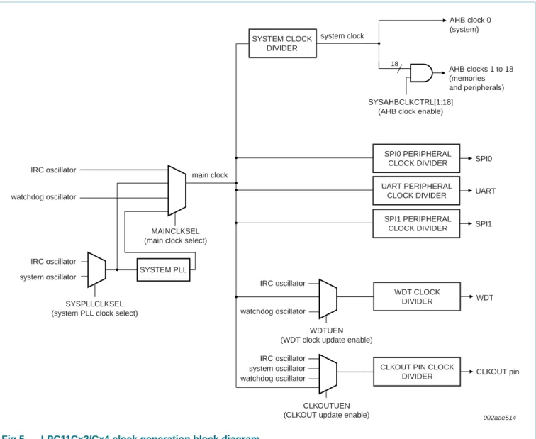
7.16.1 Crystal oscillators
The LPC11Cx2/Cx4 include three independent oscillators. These are the system
oscillator, the Internal RC oscillator (IRC), and the Watchdog oscillator. Each oscillator can be used for more than one purpose as required in a particular application.
Following reset, the LPC11Cx2/Cx4 will operate from the Internal RC oscillator until switched by software. This allows systems to operate without any external crystal and the bootloader code to operate at a known frequency.
7.16.1.1 Internal RC oscillator
The IRC may be used as the clock source for the WDT, and/or as the clock that drives the PLL and subsequently the CPU. The nominal IRC frequency is 12 MHz. The IRC is trimmed to 1 % accuracy over the entire voltage and temperature range.
Upon power-up or any chip reset, the LPC11Cx2/Cx4 use the IRC as the clock source. Software may later switch to one of the other available clock sources.
7.16.1.2 System oscillator
The system oscillator can be used as the clock source for the CPU, with or without using the PLL.
The system oscillator operates at frequencies of 1 MHz to 25 MHz. This frequency can be boosted to a higher frequency, up to the maximum CPU operating frequency, by the system PLL.
Fig 5. LPC11Cx2/Cx4 clock generation block diagram
SYSTEM PLL IRC oscillator system oscillator watchdog oscillator IRC oscillator watchdog oscillator MAINCLKSEL (main clock select)
SYSPLLCLKSEL (system PLL clock select)
SYSTEM CLOCK DIVIDER
AHB clock 0 (system)
SYSAHBCLKCTRL[1:18] (AHB clock enable)
AHB clocks 1 to 18 (memories and peripherals)
SPI0 PERIPHERAL
CLOCK DIVIDER SPI0
SPI1 PERIPHERAL
CLOCK DIVIDER SPI1 UART PERIPHERAL
CLOCK DIVIDER UART
WDT CLOCK
DIVIDER WDT
WDTUEN (WDT clock update enable)
watchdog oscillator IRC oscillator
system oscillator CLKOUT PIN CLOCK
DIVIDER CLKOUT pin
CLKOUTUEN
(CLKOUT update enable) 002aae514
main clock
system clock
IRC oscillator
7.16.1.3 Watchdog oscillator
The watchdog oscillator can be used as a clock source that directly drives the CPU, the watchdog timer, or the CLKOUT pin. The watchdog oscillator nominal frequency is programmable between 7.8 kHz and 1.7 MHz. The frequency spread over processing and temperature is 40 % (see Table 16).
7.16.2 System PLL
The PLL accepts an input clock frequency in the range of 10 MHz to 25 MHz. The input frequency is multiplied up to a high frequency with a Current Controlled Oscillator (CCO). The multiplier can be an integer value from 1 to 32. The CCO operates in the range of 156 MHz to 320 MHz, so there is an additional divider in the loop to keep the CCO within its frequency range while the PLL is providing the desired output frequency. The output divider may be set to divide by 2, 4, 8, or 16 to produce the output clock. The PLL output frequency must be lower than 100 MHz. Since the minimum output divider value is 2, it is insured that the PLL output has a 50 % duty cycle. The PLL is turned off and bypassed following a chip reset and may be enabled by software. The program must configure and activate the PLL, wait for the PLL to lock, and then connect to the PLL as a clock source. The PLL settling time is 100s.
7.16.3 Clock output
The LPC11Cx2/Cx4 features a clock output function that routes the IRC oscillator, the system oscillator, the watchdog oscillator, or the main clock to an output pin.
7.16.4 Wake-up process
The LPC11Cx2/Cx4 begin operation at power-up and when awakened from Deep power-down mode by using the 12 MHz IRC oscillator as the clock source. This allows chip operation to resume quickly. If the system oscillator or the PLL is needed by the application, software will need to enable these features and wait for them to stabilize before they are used as a clock source.
7.16.5 Power control
The LPC11Cx2/Cx4 support a variety of power control features. There are three special modes of processor power reduction: Sleep mode, Deep-sleep mode, and Deep power-down mode. The CPU clock rate may also be controlled as needed by changing clock sources, reconfiguring PLL values, and/or altering the CPU clock divider value. This allows a trade-off of power versus processing speed based on application requirements. In addition, a register is provided for shutting down the clocks to individual on-chip peripherals, allowing fine tuning of power consumption by eliminating all dynamic power use in any peripherals that are not required for the application. Selected peripherals have their own clock divider which provides even better power control.
7.16.5.1 Sleep mode
When Sleep mode is entered, the clock to the core is stopped. Resumption from the Sleep mode does not need any special sequence but re-enabling the clock to the ARM core. In Sleep mode, execution of instructions is suspended until either a reset or interrupt occurs. Peripheral functions continue operation during Sleep mode and may generate interrupts to cause the processor to resume execution. Sleep mode eliminates dynamic power used by the processor itself, memory systems and related controllers, and internal buses.
7.16.5.2 Deep-sleep mode
In Deep-sleep mode, the chip is in Sleep mode, and in addition all analog blocks are shut down. As an exception, the user has the option to keep the watchdog oscillator and the BOD circuit running for self-timed wake-up and BOD protection. Deep-sleep mode allows for additional power savings.
Up to 13 pins total, see Table 3, serve as external wake-up pins to a dedicated start logic to wake up the chip from Deep-sleep mode.
Unless the watchdog oscillator is selected to run in Deep-sleep mode, the clock source should be switched to IRC before entering Deep-sleep mode, because the IRC can be switched on and off glitch-free.
7.16.5.3 Deep power-down mode
In Deep power-down mode, power is shut off to the entire chip with the exception of the WAKEUP pin. The LPC11Cx2/Cx4 can wake up from Deep power-down mode via the WAKEUP pin.
When entering Deep power-down mode, an external pull-up resistor is required on the WAKEUP pin to hold it HIGH. The RESET pin must also be held HIGH to prevent it from floating while in Deep power-down mode.
7.17 System control
7.17.1 Start logic
The start logic connects external pins to corresponding interrupts in the NVIC. Each pin shown in Table 3 as input to the start logic has an individual interrupt in the NVIC interrupt vector table. The start logic pins can serve as external interrupt pins when the chip is running. In addition, an input signal on the start logic pins can wake up the chip from Deep-sleep mode when all clocks are shut down.
The start logic must be configured in the system configuration block and in the NVIC before being used.
7.17.2 Reset
Reset has four sources on the LPC11Cx2/Cx4: the RESET pin, the Watchdog reset, power-on reset (POR), and the BrownOut Detection (BOD) circuit. The RESET pin is a Schmitt trigger input pin. Assertion of chip reset by any source, once the operating voltage attains a usable level, starts the IRC and initializes the flash controller.
When the internal Reset is removed, the processor begins executing at address 0, which is initially the Reset vector mapped from the boot block. At that point, all of the processor and peripheral registers have been initialized to predetermined values.
An external pull-up resistor is required on the RESET pin if Deep power-down mode is used.
7.17.3 Brownout detection
The LPC11Cx2/Cx4 includes four levels for monitoring the voltage on the VDD pin. If this voltage falls below one of the four selected levels, the BOD asserts an interrupt signal to the NVIC. This signal can be enabled for interrupt in the Interrupt Enable Register in the NVIC in order to cause a CPU interrupt; if not, software can monitor the signal by reading a dedicated status register. Four additional threshold levels can be selected to cause a forced reset of the chip.
7.17.4 Code security (Code Read Protection - CRP)
This feature of the LPC11Cx2/Cx4 allows user to enable different levels of security in the system so that access to the on-chip flash and use of the Serial Wire Debugger (SWD) and In-System Programming (ISP) can be restricted. When needed, CRP is invoked by programming a specific pattern into a dedicated flash location. IAP commands are not affected by the CRP.
In addition, ISP entry via the PIO0_1 pin can be disabled without enabling CRP. For details see the LPC11Cx user manual.
There are three levels of Code Read Protection:
1. CRP1 disables access to the chip via the SWD and allows partial flash update (excluding flash sector 0) using a limited set of the ISP commands. This mode is useful when CRP is required and flash field updates are needed but all sectors can not be erased.
2. CRP2 disables access to the chip via the SWD and only allows full flash erase and update using a reduced set of the ISP commands.
3. Running an application with level CRP3 selected fully disables any access to the chip via the SWD pins and the ISP. This mode effectively disables ISP override using PIO0_1 pin, too. It is up to the user’s application to provide (if needed) flash update mechanism using IAP calls or call reinvoke ISP command to enable flash update via the UART.
In addition to the three CRP levels, sampling of pin PIO0_1 for valid user code can be disabled. For details see the LPC11Cx user manual.
CAUTION
If level three Code Read Protection (CRP3) is selected, no future factory testing can be performed on the device.
7.17.5 Bootloader
The bootloader controls initial operation after reset and also provides the means to program the flash memory. This could be initial programming of a blank device, erasure and re-programming of a previously programmed device, or programming of the flash memory by the application program in a running system.
The bootloader code is executed every time the part is reset or powered up. The loader can either execute the user application code or the ISP command handler via UART or C_CAN. A LOW level during reset applied to the PIO0_1 pin is considered as an external hardware request to start the ISP command handler. The state of PIO0_3 at reset determines whether the UART (PIO0_3 HIGH) or the C_CAN (PIO0_3 LOW) interface will be used.
The C_CAN ISP command handler uses the CANopen protocol and data organization method. C_CAN ISP commands have the same functionality as UART ISP commands.
7.17.6 APB interface
The APB peripherals are located on one APB bus.
7.17.7 AHBLite
The AHBLite connects the CPU bus of the ARM Cortex-M0 to the flash memory, the main static RAM, and the Boot ROM.
7.17.8 External interrupt inputs
All GPIO pins can be level or edge sensitive interrupt inputs. In addition, start logic inputs serve as external interrupts (see Section 7.17.1).
7.18 Emulation and debugging
Debug functions are integrated into the ARM Cortex-M0. Serial wire debug with four breakpoints and two watchpoints is supported.
8. Limiting
values
[1] The following applies to the limiting values:
a) This product includes circuitry specifically designed for the protection of its internal devices from the damaging effects of excessive static charge. Nonetheless, it is suggested that conventional precautions be taken to avoid applying greater than the rated maximum.
b) Parameters are valid over operating temperature range unless otherwise specified. All voltages are with respect to VSS unless otherwise noted.
[2] Maximum/minimum voltage above the maximum operating voltage (see Table 6) and below ground that can be applied for a short time (<10 ms) to a device without leading to irrecoverable failure. Failure includes the loss of reliability and shorter lifetime of the device. [3] Including voltage on outputs in 3-state mode.
[4] The peak current is limited to 25 times the corresponding maximum current.
[5] The maximum non-operating storage temperature is different than the temperature for required shelf life which should be determined based on required shelf lifetime. Please refer to the JEDEC spec (J-STD-033B.1) for further details.
[6] Human body model: equivalent to discharging a 100 pF capacitor through a 1.5 k series resistor.
Table 5. Limiting values
In accordance with the Absolute Maximum Rating System (IEC 60134).[1]
Symbol Parameter Conditions Min Max Unit
VDD supply voltage (core
and external rail)
on pins VDD [2] 0.5 4.6 V
VI input voltage 5 V tolerant I/O pins; VDD 1.8 V [3] 0.5 +5.5 V
Vx voltage on pin x no time limit; DC value
on pins CANH and CANL 58 +58 V
on pins STB, VCC, VDD_CAN 0.3 +7 V
IDD supply current per supply pin [4] - 100 mA
ISS ground current per ground pin [4] - 100 mA
Ilatch I/O latch-up current (0.5VDD) < VI < (1.5VDD);
Tj < 125C
- 100 mA
Tstg storage temperature non-operating [5] 65 +150 C
Tj(max) maximum junction temperature
- 150 C
Ptot(pack) total power dissipation (per package)
based on package heat transfer, not device power consumption
- 1.5 W
VESD electrostatic discharge
voltage
human body model;
all pins except CAN on-chip transceiver pins CANL, CANH, STB, VDD_CAN, VCC, GND on
LPC11C22/C24
[6] 6500 +6500 V
pins CANH and CANL on LPC11C22/C24 [6] 8000 +8000 V
pins STB, VDD_CAN, VCC, GND on
LPC11C22/C24
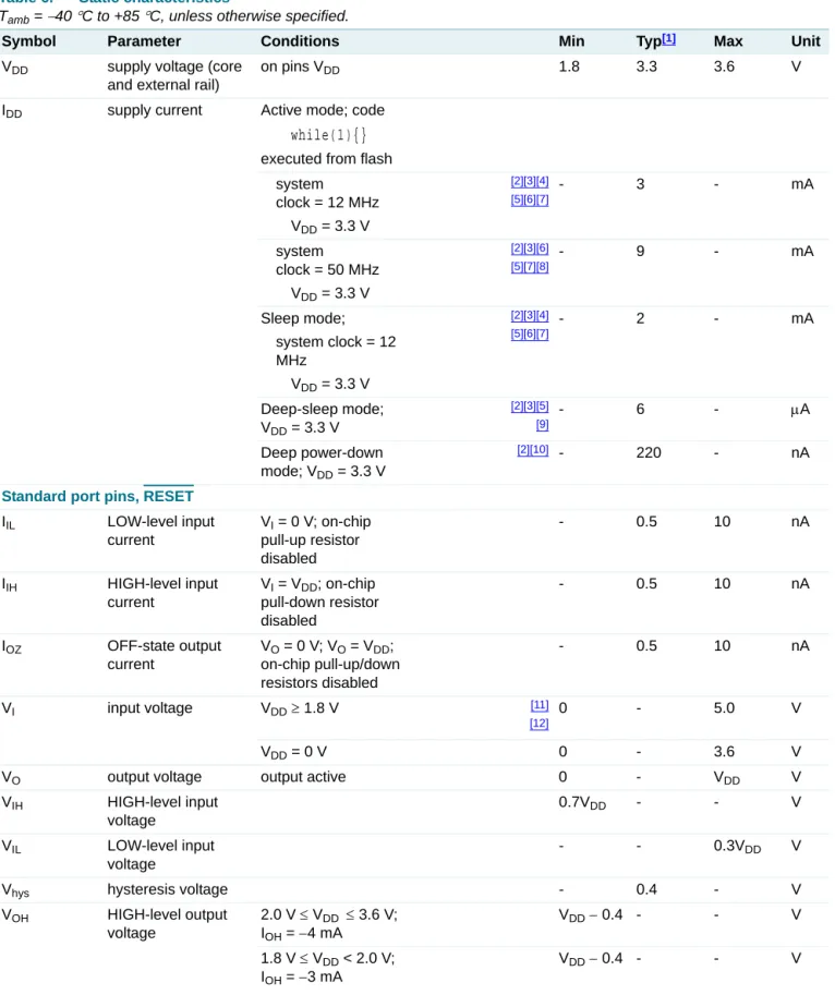
9. Static
characteristics
Table 6. Static characteristics
Tamb=40C to +85C, unless otherwise specified.
Symbol Parameter Conditions Min Typ[1] Max Unit
VDD supply voltage (core
and external rail)
on pins VDD 1.8 3.3 3.6 V
IDD supply current Active mode; code
while(1){}
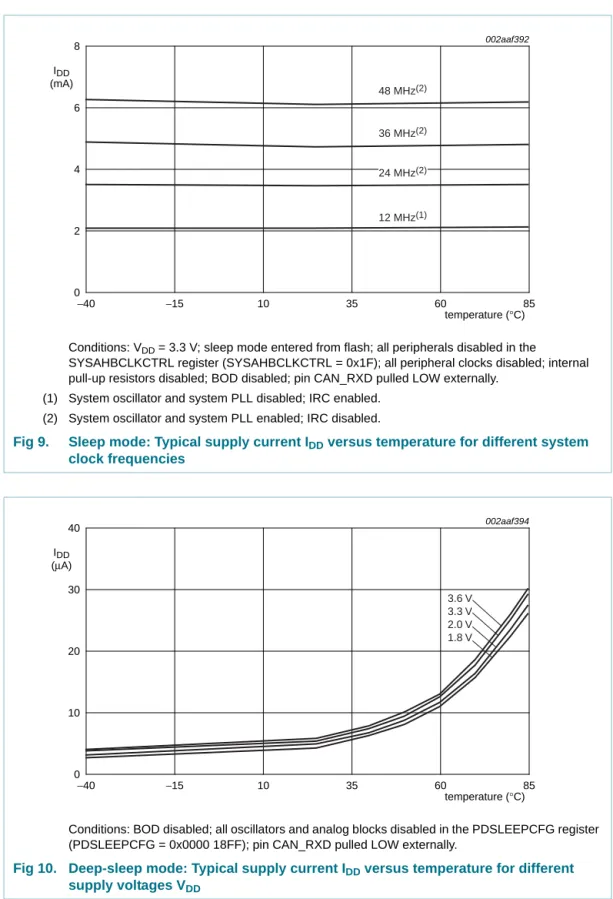
executed from flash system clock = 12 MHz VDD = 3.3 V [2][3][4] [5][6][7] - 3 - mA system clock = 50 MHz VDD = 3.3 V [2][3][6] [5][7][8] - 9 - mA Sleep mode; system clock = 12 MHz VDD = 3.3 V [2][3][4] [5][6][7] - 2 - mA Deep-sleep mode; VDD = 3.3 V [2][3][5] [9] - 6 - A Deep power-down mode; VDD = 3.3 V [2][10] - 220 - nA
Standard port pins, RESET
IIL LOW-level input
current VI= 0 V; on-chip pull-up resistor disabled - 0.5 10 nA IIH HIGH-level input current VI= VDD; on-chip pull-down resistor disabled - 0.5 10 nA
IOZ OFF-state output
current VO= 0 V; VO= VDD; on-chip pull-up/down resistors disabled - 0.5 10 nA VI input voltage VDD 1.8 V [11] [12] 0 - 5.0 V VDD = 0 V 0 - 3.6 V
VO output voltage output active 0 - VDD V
VIH HIGH-level input voltage 0.7VDD - - V VIL LOW-level input voltage - - 0.3VDD V
Vhys hysteresis voltage - 0.4 - V
VOH HIGH-level output
voltage 2.0 V VDD 3.6 V; IOH=4 mA VDD 0.4 - - V 1.8 V VDD < 2.0 V; IOH=3 mA VDD 0.4 - - V
VOL LOW-level output voltage 2.0 V VDD 3.6 V; IOL= 4 mA - - 0.4 V 1.8 V VDD < 2.0 V; IOL= 3 mA - - 0.4 V
IOH HIGH-level output
current
VOH= VDD0.4 V;
2.0 V VDD 3.6 V
4 - - mA
1.8 V VDD < 2.0 V 3 - - mA
IOL LOW-level output
current VOL= 0.4 V 2.0 V VDD 3.6 V 4 - - mA 1.8 V VDD < 2.0 V 3 - - mA IOHS HIGH-level short-circuit output current VOH= 0 V [13] - - 45 mA IOLS LOW-level short-circuit output current VOL= VDD [13] - - 50 mA
Ipd pull-down current VI= 5 V 10 50 150 A
Ipu pull-up current VI= 0 V;
2.0 V VDD 3.6 V
15 50 85 A
1.8 V VDD < 2.0 V 10 50 85 A
VDD< VI< 5 V 0 0 0 A
High-drive output pin (PIO0_7)
IIL LOW-level input current VI= 0 V; on-chip pull-up resistor disabled - 0.5 10 nA
IIH HIGH-level input
current VI= VDD; on-chip pull-down resistor disabled - 0.5 10 nA IOZ OFF-state output current VO= 0 V; VO= VDD; on-chip pull-up/down resistors disabled - 0.5 10 nA VI input voltage VDD 1.8 V [11] [12] 0 - 5.0 V VDD = 0 V 0 - 3.6 V
VO output voltage output active 0 - VDD V
VIH HIGH-level input
voltage
0.7VDD - - V
VIL LOW-level input
voltage
- - 0.3VDD V
Vhys hysteresis voltage 0.4 - - V
VOH HIGH-level output voltage 2.5 V VDD 3.6 V; IOH=20 mA VDD 0.4 - - V 1.8 V VDD < 2.5 V; IOH=12 mA VDD 0.4 - - V
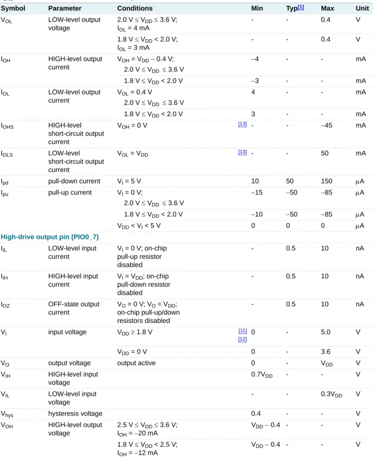
Table 6. Static characteristics …continued
Tamb=40C to +85C, unless otherwise specified.