1
Introduction to
Modulators:
Basic Concepts and Fundamentals
This chapter is conceived as an introduction to analog-to-digital converters (ADCs). Their operation principle consists in combining oversampling, quantization error process-ing, and negative feedback for improving the effective resolution of a coarse quantizer. These basic concepts are presented in Section 1.1 and their effects on the performance of converters are compared with Nyquist-rate converters. Section 1.2 shows the basic architecture, ideal behavior, and performance metrics ofconverters, and sketches the architectural alternatives to enhance their resolution.Before presenting practical topologies for the implementation of modulation, the large variety of the existingrealizations is briefly classified in Section 1.3 according to the type of modulator architecture (single loops or cascades), the circuit techniques employed (discrete time (DT) or continuous time (CT)), and the nature of the signals being converted (low pass (LP) or band pass (BP)). Starting from the case of DT, LP, single-bit modulators, the implications of these different alternatives are then presented in an incremental way.
Section 1.4 is dedicated to single-loop architectures. Second- and higher-order single-loops are considered, taking into account issues related to their practical implemen-tation and problems not addressed by linear models, such as instabilities. Cascade topologies are covered in Section 1.5. In Section 1.6 the topological study is extended to modulators using multibit embedded quantizers, analyzing their pros and cons. Techniques to circumvent the disadvantages, such as dynamic element matching (DEM) or dual quantization, are revised.
The conversion of BP signals is covered in Section 1.7, taking into account its typical application in digital radio receivers. The basic techniques for synthesizing DT, BP modulators are presented, together with practical aspects for their implementation. Finally, Section 1.8 addresses the realization of CT modulators, discussing their advantages compared to DT ones and the existing alternatives for the loop filter and the feedback implementation.
CMOS Sigma-Delta Converters: Practical Design Guide, First Edition. Jos´e M. de la Rosa and Roc´ıo del R´ıo.
©2013 John Wiley & Sons, Ltd. Published 2013 by John Wiley & Sons, Ltd.
1.1
Basics of A/D Conversion
ADCs are electronic systems that perform the transformation of analog signals—which are continuous in time and in amplitude—into digital signals—which are discrete in both time and amplitude. Figure 1.1 illustrates the general block diagram of an ADC intended for the conversion of LP signals, which essentially consists of anantialiasing filter(AAF), asampler, and aquantizer. First, the analog input signalxa(t)of the ADC passes through the AAF, an LP analog filter than prevents out-of-band components from folding over the signal bandwidth Bw during the subsequent sampling, what would corrupt the signal information. The resulting band-limited signal x(t) is sampled at a rate fs by the S/H circuit, thus yielding a DT signalxs(n)=x(nTs), whereTs=1/fs. Finally, the values of xs(n)are quantized usingN bits, so that each continuous-valued input sample is mapped onto the closer discrete-valued level out of the 2N that cover the input range, yielding the converter digital output yd(n).
As shown in Figure 1.1, the fundamental processes involved in the A/D conversion are sampling and quantization, whose implications are discussed in the following text.
1.1.1 Sampling
The sampling process performs the continuous-to-discrete transformation of the input signal in time and imposes a limit on the bandwidth of the analog input signal. According to the Nyquist theorem, to prevent information loss,x(t)must be sampled at a minimum rate offN=2Bw, often referred to as theNyquist frequency. On the basis of this criterion, ADCs in which analog input signal is sampled at the minimum rate (fs=fN) are called Nyquist-rate ADCs. Conversely, ADCs in whichfs> fN are calledoversampling ADCs. How much faster than required the input signal is sampled is expressed in terms of the oversampling ratio(OSR), defined as
OSR= fs
2Bw (1.1)
Whether oversampling is used or not in an ADC has a noticeable influence on the requirements of its AAF. As in Nyquist-rate ADCs the input signal bandwidth Bw coin-cides withfs/2, aliasing will occur ifxa(t)in Figure 1.1 contains frequency components above fs/2. High-order analog AAFs are thus required to implement sharp transition bands capable of removing out-of-band components with no significant attenuation of the signal band, as illustrated in Figure 1.2a for the LP case. Conversely, as fs/2> Bw in oversampling ADCs, the replicas of the input signal spectrum that are created by the sampling process are farther apart than in Nyquist-rate ADCs. As illustrated in Figure 1.2b,
N xa(t) Bw fs x(t) xs(n) N-bit
Antialiasing filter Quantizer
S/H yd(n)
−fs/2 −fs/2 −Bw +fs/2 +fs +fs/2 +fs Xa(f) Xa(f) f f −fs −fs HAAF(f) HAAF(f) (a) +Bw (b)
Figure 1.2 Antialiasing filter for (a) Nyquist-rate ADCs and (b) oversampling ADCs.
frequency components of the input signal in the range [Bw, fs−Bw] do not alias within the signal band, so that the filter transition band can be smoother, what greatly reduces the order required for the AAF and simplifies its design.
1.1.2 Quantization
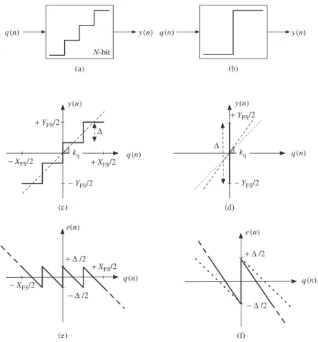
The quantization process also introduces a limitation on the performance of an ideal ADC, because an error is generated while performing the continuous-to-discrete transformation of the input signal in amplitude, commonly referred to asquantization error. The operation of quantizers is illustrated in Figure 1.3. As a matter of example, Figure 1.3c depicts the I/O characteristic of a quantizer with N=2, although results apply to a generic N-bit quantizer. Input amplitudes within the full-scale input range [−XFS/2,+XFS/2] are roundedto 1 out of the 2N different output levels, which are usually encoded into a binary digital representation. If these levels are equally spaced, the quantizer is said to beuniform and the separation between adjacent output levels is defined as thequantization step
= YFS
2N−1 (1.2)
where YFS stands for the full-scale output range. As XFS and YFS are not necessarily equal, the quantizer may exhibit a gain different from unity, as indicated in Figure 1.3c by the slope kq. As shown in Figure 1.3e, the quantizer operation thus inherently generates a roundingerror that is a nonlinear function of the input. Note that, ifq(n) is kept within the range [−XFS/2,+XFS/2], the quantization error e(n)is bounded within [−/2,+/2]. The former input range is known as the nonoverload region of the quantizer, as opposed to ranges with |q(n)|> /2, for which the magnitude of e(n) grows monotonously.
Δ Δ (a) (b) (c) (d) (e) (f) q(n) q(n) q(n) q(n) q(n) q(n) kq kq y(n) y(n) + YFS/2 + Δ /2 + Δ /2 − Δ /2 − Δ /2 + YFS/2 + XFS/2 + XFS/2 − YFS/2 − XFS/2 − XFS/2 − YFS/2 y(n) e(n) e(n) y(n) N-bit
Figure 1.3 Illustration of the quantization process: (a) multibit quantizer block, (b) single-bit quantizer block, (c) I/O characteristic of a multibit quantizer, (d) I/O characteristic of a single-bit quantizer, (e) multibit quantization error, and (f) single-bit quantization error.
Figure 1.3 also shows the operation of a single-bit quantizer (N=1). Note from Figure 1.3d that, compared to the multibit case, the output of a single-bit quantizer is determined by the input sign only, regardless of its magnitude. Therefore, the gainkq is undefined and can be arbitrarily chosen.
1.1.3 Quantization White Noise Model
In practice, an ideal quantizer as that shown in Figure 1.4a is often modeled using the linear scheme in Figure 1.4b if several assumptions are made on the statistical properties of the quantization error [1–3]. As already shown in Figure 1.3e, the quantization error e(n)is systematically determined by the quantizer input signalq(n). Nevertheless, ifq(n) is assumed to change randomly from sample to sample within the range [−/2,+/2], e(n)will also be uncorrelated from sample to sample. Under these requirements, the quan-tization error can be viewed as arandom process with a uniform probability distribution
Δ 12fs −fs/ 2 +fs/ 2 f (b) (a) (c) (d) q(n) y e e N-bit PDF(e) S E(f) 1/Δ −Δ / 2 +Δ / 2 kq y(n)
Figure 1.4 Quantization noise: (a) multibit quantizer block, (b) equivalent linear model with additive white noise, (c) probability density function (PDF), and (d) power spectral density.
in the range [−/2,+/2], as illustrated in Figure 1.4c. The power associated to the quantization error can thus be computed as
e2=σ2 e= +∞ −∞ e2PDF(e)de= 1 +/2 −/2 e2de= 2 12 (1.3)
The former assumption implies that, as illustrated in Figure 1.4d, the power of the quan-tization error will also be uniformlydistributed in the range [−fs/2,+fs/2], yielding
e2 = +∞ −∞ SE(f )df =SE +fs/2 −fs/2 df = 2 12 (1.4)
so that the power spectral density (PSD) of the quantization error in that range is SE= e
2
fs = 2
12fs (1.5)
These assumptions are collectively known as theadditive white noise approximationof the quantization error and allow the representation of a quantizer, which is deterministic and nonlinear, with the random linear model in Figure 1.4b, in which y(n)=kqq(n)+e(n) with e(n)being aquantization noise.1
On the basis of this approximation of the quantization error to a white noise, the performance of ideal ADCs can be easily evaluated. For a Nyquist ADC, in which
1Although the assumptions underlying the additive white noise approximation are hardly met in practice and are
not strictly valid, it is commonly used in ADC design and usually yields good results—the larger the number of bits in the quantizer, the better. Even though strictly speaking, it is not valid for stand-alone single-bit quantizers, it is also employed in the design of single-bitmodulators [4].
−fs/ 2 +fs/ 2 +fs/ 2 −fs/ 2 X (f) f +fs +fs −fs −fs IBN = Δ 2 IBN = 12 Δ2 12OSR SE= Δ 2 12fs (a) (b) f −Bw +Bw X(f) SE= Δ 2 12fs
Figure 1.5 Quantization noise in (a) Nyquist-rate ADCs and (b) oversampling ADCs.
fs=2Bw, all the quantization noise power falls inside the signal band and passes to the ADC output as a part of the input signal itself, as illustrated in Figure 1.5a. Con-versely, if an oversampled signal is quantized, becausefs>2Bw, only a fraction of the total quantization noise power lies within the signal band, as illustrated in Figure 1.5b. The in-band noise power (IBN) caused by the quantization process in an ideal oversampling ADC is thus, IBN= +Bw −Bw SE(f )df = +Bw −Bw 2 12fs df = 2 12OSR (1.6)
so that the larger the OSR, the smaller the IBN.2
Thedynamic range(DR) of an ideal ADC can be determined as the ratio of the output power at the frequency of an input sinusoid with maximum amplitude to the in-band quantization noise power:
DR(dB)=10log10 P sig,out,max IBN (1.7) From Figure 1.3c, the maximum input amplitude in the nonoverload region of an N-bit quantizer is XFS/2 and its corresponding output power can be approximated to [5],
Psig,out,max≈ (2
N
/2)2
2 =2
2N−32 (1.8)
so that, using Equations 1.6 and 1.8, the DR of an ideal oversampling ADC yields
DR(dB)≈6.02N+1.76+10log10(OSR) (1.9)
2Note that Equation 1.6 for the IBN of oversampling ADCs also holds true for Nyquist ADCs, just considering
f +fs −fs −fs/2 −Bw +Bw +fs/2 X(f) IBN SE|NTF(f)|2 (a) (b) q(n) NTF(z) eshaped(n) N-bit y(n) e(n)
Figure 1.6 Quantization noise shaping: (a) conceptual block diagram and (b) effect on the in-band noise of an oversampling noise-shaping ADC.
Note that, for a Nyquist ADC—that is, OSR=1 in Equation 1.9—each additional bit in the quantizer results in a DR increase of approximately 6 dB. For an oversampling ADC, the DR further increases with the OSR by approximately 3 dB/octave, so that using for instance an OSR of 4 is similar to having one extra bit in the N-bit quantizer.
1.1.4 Noise Shaping
An approach to further increase the accuracy of an oversampling ADC is shaping the quantization white noise in the frequency domain—that is, filtering it—in such a way that most of its power lies outside the signal band. This is illustrated in Figure 1.6a, where the quantization noise is conceptually obtained by subtracting the quantizer input signal q(n)from its outputy(n)and then passes through a filter transfer function, usually called noise transfer function (NTF).
For quantizers working on LP signals, the NTF is of high-pass type and can be easily obtained from a differentiator filter, with a Z-domain transfer function given by
NTF(z)=(1−z−1)L (1.10)
where L stands for the filter order. Taking into account that z=esTs=ej2πf/fs, the magnitude of the pure-differentiator NTF in Equation 1.10 can be approximated for low frequencies to |NTF(f )| = |1−e−j2πf/fs|L= 2 sin πf fs L ≈ 2πf fs L , for f fs (1.11)
so that the power due to the shaped quantization noise that lies within the signal band (Figure 1.6b) yields IBN= +Bw −Bw SE(f )|NTF(f )|2 df ≈ 2 12 π2L (2L+1)OSR(2L+1) (1.12) Using Equations 1.8 and 1.12, the DR of an ideal oversampling noise-shaping ADC can be obtained as DR(dB)≈6.02N+1.76+10log10 2L+1 π2L +(2L+1)10log10(OSR) (1.13) Note that, in comparison with Equation 1.9, if oversampling is used in combination with noise shaping, the DR increases with OSR by approximately 3(2L+1)dB/octave.
1.2
Basics of Sigma-Delta Modulators
Contrary to the ADCs discussed so far, which are open loop systems from a control perspective, Sigma-Delta () ADCs rely on a feedback path to achieve a closed-loop control of the quantization error. The fundamentals on how the shaping of quantization noise is implemented in practice, as well as the basic architecture, performance metrics, and ideal behavior of oversampling noise-shaping ADCs is presented in the following sections.
1.2.1 Topology of
ADCs
Figure 1.7 illustrates the basic block diagram of a ADC intended for the conversion of LP signals, which consists of the following:
• Antialiasing filter (AAF), which band limits the analog input signal to avoid aliasing during its subsequent sampling. As discussed in Section 1.1.1, oversampling consider-ably relaxes the attenuation requirements of the AAF, so that smooth transition bands are usually sufficient compared to Nyquist-rate ADCs.
• Sigma-Delta modulator (M), in which the oversampling and quantization of the band-limited analog signal take place. The quantization noise of the embedded B-bit quantizer is shaped in the frequency domain by placing an appropriate loop filterH (z) before it and closing a negative feedback loop around them. Low-resolution quantizers, with B typically in the range 1–5 bit, are sufficient for obtaining small IBN and high accuracy in the A/D conversion.
• Decimation filter, in which a high-selectivity digital filter sharply removes the out-of-band spectral content of the M output and thus most of the shaped quantization noise. The decimator also reduces the data rate fromfsdown to the Nyquist frequency, while increasing the word length fromB toN bits to preserve resolution.
The modulator is the block that has most influence on the performance of the ADC, basically because it is responsible for the sampling and quantization processes that
xa(t) x(t) y(n) yd(n) Bw fs−Bw Antialiasing filter LP filter Sigma-delta modulator Decimator OSR Downsampler Digital filter S/H ADC B @fs N @fN Bw DAC H(z) B-bit Quantizer fs
Figure 1.7 General block diagram of aADC. A low-pass discrete-timeM is assumed.
(a) x(n) (b) x(n) q(n) q(n) y(n) y(n) e(n) kq H(z) H(z) B-bit
Figure 1.8 modulator: (a) block diagram and (b) ideal linear model.
ultimately limit the accuracy of the A/D conversion. We will focus on this block from now on, although it must be kept in mind that aADC is more than aM!
1.2.2 Signal Processing in
Ms
The basic scheme of amodulator consists of a loop filterH (z)and aB-bit quantizer in a feedback loop, as shown in Figure 1.8a [6]. Let us consider that the gain of the loop filter is large within the signal band and small outside it. Owing to the action of negative feedback, the analog input signal x and the analog version of the M output y will practically coincide within the signal band, so that the error signal x−y in this closed-loop system is very small within the signal band. As theB-bit quantizer is uniform, most of the differences between the input and the output of theM will be placed at higher frequencies, so that the quantization noise is shaped in the frequency domain and most of its power is pushed outside the signal band.
Using the linear additive white noise model in Figure 1.4b for the embedded quantizer, theM in Figure 1.8a can be modeled as the two-input (xande) one-output (y) linear system in Figure 1.8b, which is described in theZ-domain as
where STF and NTF stand for the signal and noise transfer functions, respectively given by STF(z)= kqH (z) 1+kqH (z) , NTF(z)= 1 1+kqH (z) (1.15)
Note that, if the loop filter is designed such that|H (f )| 1 within the signal band, then |STF(f )| ≈1 and|NTF(f )| 1; that is, the quantization noise is ideally canceled while the input signal is perfectly transferred to the output.
For the conversion of LP signals, the simplest loop filterH (z)that exhibits the desired frequency performance is an integrator,
ITF(z)= z −1
1−z−1 (1.16)
that, in combination with an embedded quantizer with kq=1, leads to a M whose output is given by
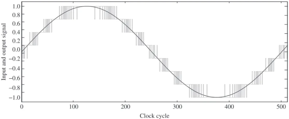
Y (z)=z−1X(z)+(1−z−1)E(z) (1.17)
and builds up a first-order, high-pass shaping of the quantization noise—see Equation 1.10. For the sake of illustration, Figure 1.9 shows the output signal of a first-orderM with a embedded 3-bit (8-level) quantizer for a sinusoidal input signal. Note that, due to the combined action of oversampling and negative feedback, the modulator output is a pulse-density modulated (PDM) signal whose local average tracks the input signal value within adjacent code transitions.
1.2.3 Performance Metrics of
Ms
Contrary to Nyquist-rate ADCs, whose performance is mainly characterized by static performance metrics—that is, monotonicity, gain and offset errors, differential nonlinear-ity (DNL), and integral nonlinearnonlinear-ity (INL) [5]— ADCs’ characteristics are typically
1.0 0.8 0.6 0.4 0.2 0.0 −0.2 −0.4 −0.6 0 100 200 Clock cycle 300 400 500 −0.8 −1.0
Input and output signal
Figure 1.9 PDM output signal of a first-order,modulator with an embedded 3-bit quantizer for an input sinusoid.
−40 −60 −80 −100 −120 −140 −160 −180 −200 PSD (dB) Signal peak SFDR fin 3fin Harmonics Noise floor 256-k point FFT Bw 10−4 10−3 Normalized frequency, f/fs 10−2 10−1 100
Figure 1.10 Illustration of a typical output spectrum of amodulator and its main character-istics. A low-passM is assumed.
measured using dynamic performance metrics, which are obtained from the frequency-domain representation of the time-frequency-domain digital output sequence. The latter thus requires the computation of the fast Fourier transform (FFT) of a finite-length output sequence with a specific windowing function, as will be discussed in Chapter 4. From that power spectrum representation of a M output sequence, some spectral metrics are directly measured and other noise and power metrics are derived.
Figure 1.10 illustrates an exemplary spectrum of a M output sequence when a sinusoidal signal with frequencyfin is applied at its input. The main characteristics of the spectrum are highlighted; for example, the length of the digital sequence from which the FFT has been computed, the output signal peak at the frequencyfincorresponding to the converted signal, etc. As will be discussed in Chapter 2, nonidealities of the circuitry used for implementing theM deviate in practice the output spectrum from apurelyshaped quantization noise. On the one hand, linear errors give rise to a noise floor, as well as to a degradation of the shaping order. On the other, nonlinear errors generate distortion, which is typically noticeable for large input amplitudes, butsubmergedunder the noise floor for small input signal amplitudes. Spectral metrics such as the spurious-free dynamic range (SFDR)—that is, the ratio of the signal power to the strongest spectral tone [5]—can be directly measured from the output modulator spectrum, as shown in Figure 1.10.
Noise and power metrics are derived from theM output spectra by integration over the signal bandwidth and are typically collected in a single plot as shown in Figure 1.11. These metrics are usually the most important measures and comprise the following: • Signal-to-noise ratio(SNR), which is the ratio of the output power at the frequency of
an input sinusoid to theuncorrelatedIBN: SNR(dB)=10log10 P sig,out IBN (1.18)
SNR, SNDR (dB) DR
SNRpeak SNDRpeak
Input signal amplitude, Ain (dBV) 0
XOL
Xmin XFS/2
Figure 1.11 Illustration of the performance metrics of amodulator on a typical SNR curve.
It accounts for the modulator linear performance only, so that the in-band power asso-ciated to harmonics of the input signal is not considered as part of the IBN for SNR computation.
If an idealM is considered and only the in-band quantization noise is accounted for in the IBN computation, the termsignal-to-quantization-noise ratio(SQNR) is often employed.
• Signal-to-noise-plus-distortion ratio(SNDR), which is defined as the ratio of the output power at the frequency of an input sinusoid to the total IBN power, also accounting for possible harmonics at theM output. As illustrated in Figure 1.11, this makes a typical SNDR curve to deviate from the SNR curve only for large input amplitudes, for which the generated distortion is noticeable. Therefore, the output spectra from which the SNDR curve is computed are typically obtained by applying an input signal at fin≤Bw/3 (for LPMs), so that at least the second and third harmonics lie within the signal band.
• Dynamic range (DR), which can be defined as the ratio of the output power at the frequency of an input sinusoid with maximum amplitude to the output power for a small input amplitude for which SNR=0 dB; that is, so it cannot be distinguished from the error. Ideally, a sinusoid with maximum amplitude at the modulator input will provide an output sinusoid sweeping the full-scale range YFS of the embedded quantizer, so that DR(dB)=10log10 P sig,out,max IBN =10log10 (YFS/2)2 2IBN (1.19) • Effective number of bits (ENOB): as the DR of an ideal N-bit Nyquist-rate con-verter is given by Equation 1.9 with OSR=1, a similar expression can be established
forMs
ENOB(bit)= DR(dB)−1.76
where ENOB can be defined as the number of bits needed for an ideal Nyquist-rate ADC to achieve the same DR as theADC. The performance of oversampled converters and Nyquist-rate ADCs can thus be compared in a simple way [7].
Instead of the DR, the peak SNDR is also often used in Equation 1.20 to express the accuracy of the A/D in a modulator in bits.
• Overload Level(OL): as illustrated in Figure 1.11, the SNR of amodulator increases monotonously with the input signal amplitude (Ain), but sharply drops for input ampli-tudes close to half of the full-scale input range of the embedded quantizer (XFS/2) due to its overload and the associated IBN increase. The overload level is considered to define the maximum input amplitude for which theM still operates correctly and can almost be arbitrarily defined, but it is typically chosen as the amplitude for which the SNR drops 6 dB below the peak SNR [8].
1.2.4 Performance Enhancement of
Ms
The output of an ideal LP Lth-order modulator in theZ-domain can be considered to be
Y (z)=STF(z)X(z)+NTF(z)E(z)=z−LX(z)+(1−z−1)LE(z) (1.21) where |STF(f )| =1 and the NTF builds up anLth-order high-pass shaping of the quan-tization noise of the embedded quantizer. If aB-bit quantizer is employed, the DR of the M can be obtained from Equations 1.12 and 1.19 to ideally yield
DR(dB)=10log10 P sig,out,max IBN ≈10log10 3 2(2 B− 1)2(2L+1)OSR (2L+1) π2L (1.22) taking into account that YFS=(2B−1)—see Equation 1.2 —and considering quanti-zation noise as the only contribution to the IBN.
Note from Equation 1.22 that the DR of a modulator is ideally determined by the values of L, OSR, and B, which can thus be considered as the three key param-eters that define the M at the high level. The pros and cons of increasing the DR of a modulator by increasing each of these parameters are briefly discussed in the following:
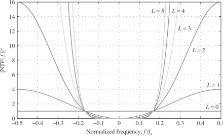
• High-ordermodulators. The accuracy of the A/D conversion can be considerably improved by increasing the noise-shaping order, because a larger fraction of the total quantization noise power will be pushed out of the signal band. Figure 1.12 illustrates the ideal noise-shaping functions of orders ranging from 1 to 5. The caseL=0—that is, no shaping—is also included for comparison purposes. The DR enhancement if L is increased in one for a given OSR can be obtained from Equation 1.22 to be
DR(dB)≈10log10 2L+3 2L+1 OSR π 2 (1.23) This means that, for instance, the DR of a fourth-orderM with OSR=32 is ideally 21.3 dB (3.5 bit) larger than that of a third-orderM.
−00.5 −0.4 −0.3 −0.2 −0.1 0 0.1 0.2 0.3 0.4 0.5 2 4 6 8 10 12 14 16 Normalized frequency, f /fs | NTF( f ) | 2 L= 0 L= 1 L= 2 L= 3 L= 4 L= 5
Figure 1.12 Illustration of the shaping of quantization noise as a function of frequency in aM. NTF is given by Equation 1.10 andLstands for the noise-shaping order.
However, as will be discussed in Section 1.4.2, the use of high-order (L >2) loop filters gives rise to stability problems in a M. Although these problems can be circumvented, the DR of a high-order M will in practice be smaller than predicted in Equation 1.22.
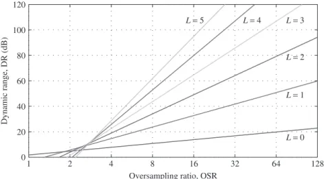
• High OSR modulators. Figure 1.13 shows the ideal DR as a function of OSR for noise-shaping orders ranging from 0 (no shaping) to 5 and assuming a single-bit embedded quantizer (B =1). As illustrated, the combination of oversampling and noise-shaping considerably enhances theM performance for OSR>4. Note from Equation 1.22 that the DR of an idealLth-ordermodulator increases with OSR in 3(2L+1)dB/octave.
However, for a given conversion bandwidth Bw, the OSR cannot be arbitrarily increased, because it leads to a higher sampling frequency fs for the operation of thecircuitry. The latter, if achievable in practice for a given technological process, leads to larger power consumption.
• Multibit modulators. An increase in B leads to a decrease of the quantization step and thus to a reduction of the quantization noise power. Each additional bit in the embedded quantizer of a M is considered to typically yield a 6 dB (1 bit) improvement on the DR [9].
However, a multibit embedded quantizer requires a multilevel DAC to close the negative feedback loop in the M. Contrary to a two-level feedback DAC (B=1), which is inherently linear, a multilevel DAC will in practice be nonlinear to some extent. As noticeable from Figure 1.17, the DAC nonlinearity will be directly added to the M input and will thus appear at the output, as|STF(f )| ≈1 within the signal band. Therefore, the linearity required in a multibit DAC equals in practice that wanted for the modulator. This point will be further discussed in Section 1.6.
120 100 80 60 40 Dynamic range, DR (dB)
Oversampling ratio, OSR 20 0 1 2 4 8 16 32 64 128 L= 5 L= 4 L= 3 L= 2 L= 1 L= 0
Figure 1.13 Ideal dynamic range of aM as a function of the oversampling ratio for different noise-shaping orders (L). A single-bit internal quantizer (B=1) is assumed.
1.3
Classification of
Modulators
The strategies discussed in Section 1.2.4 for improving the DR of a M may be combined in many different ways, giving rise to the huge number of M topolo-gies reported in literature, which can be grouped attending to different classification criteria [10]:
• Single-Loop versus CascadeMs (attending to the number of quantizers employed). Ms employing only one quantizer are calledsingle-looptopologies, whereas those employing several quantizers are often namedcascadeor MASH Ms. These topo-logical alternatives will be discussed in Sections 1.4 and 1.5.
• Single-Bit versus Multibit Ms (attending to the number of bits in the embedded quantizer). Their pros and cons will be discussed in Section 1.6.
• Low-Pass versus Band-PassMs (attending to the nature of the signals being con-verted). The A/D conversion of LP signals has been assumed in previous sections, but BPMs can also be built, as will be discussed in Section 1.7.
• Discrete-Time versus Continuous-Time Ms (attending to the nature of loop filter dynamics). The use of a DT loop filter in the M has been assumed in previous sections. However, CTMs can be also implemented in practice. According to this classification criteria,hybridCT/DTMs take advantage of the benefits of both DT and CT implementations, which will be discussed in Section 1.8.
Describing all possibleM architectures derived from previous classification criteria goes beyond the scope of this book. A detailed analysis of them can be found in the many papers and books devoted to the topic in theliterature [4, 9, 11–23]. Instead, we will hereafter focus on the most representative families of modulators.
1.4
Single-Loop
Modulators
modulators that make use of only one embedded quantizer are usually referred to as single-loop topologies. To get familiar with these architectures, their performance, their circuit-level implementation, as well as some other practical aspects are first addressed considering the case of second-orderMs. Afterward, the problematics of stability in higher-orderMs is presented, together with architectural alternatives to circumvent it.
1.4.1 Second-Order
M
Figure 1.14a shows a second-order modulator built up by cascading two DT inte-grators [24], with each integrator receiving a weighted feedback path from the DAC. Coefficientsaiare usually called integratorscalingsorweights. Under linear analysis, the modulator output in theZ-domain yields
Y (z)= kqa1a2( z−2 1−z−1)2X(z)+E(z) 1+kqa1a2( z−2 1−z−1)2 +kqa2 z−1 (1−z−1) (1.24)
where kq stands for the gain of the quantizer. For a pure second-order shaping, Equation 1.24 needs to be simplified to
Y (z)=z−2X(z)+(1−z−1)2E(z) (1.25) so that the following expressions for the integrator coefficients need to be fulfilled:
kqa1a2=1
kqa2 =2 (1.26)
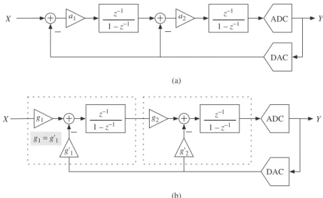
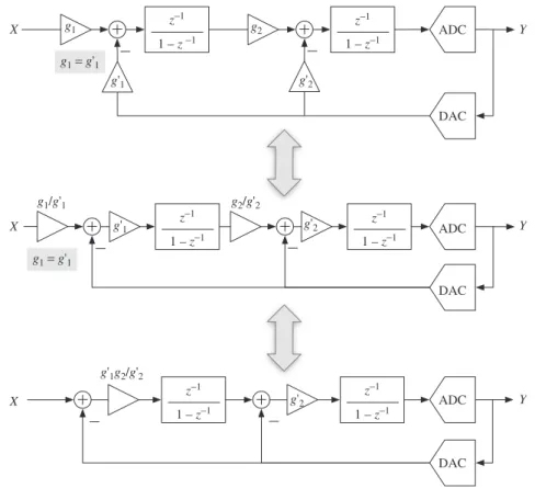
Figure 1.14b shows an alternative representation of the second-orderM according to the coefficients notation in [12, 19], which allows to allocate different weights in the forward and feedback paths of each integrator, using coefficientsgi andgi, respectively. As exemplary illustrated in Figure 1.15, the notations in Figure 1.14a and b can be easily connected with the equalities:
a1 = g 1g2 g2 a2 =g2 (1.27)
Both nomenclatures for the integrator scaling coefficients of modulators will be used throughout this book. The notation in [8, 9] is closer to the modulator architectural level, whereas the notation in [12, 19] is closer to the actual circuit-level implementation, in which integrators with more than one SC input branch are usually employed. The latter is thus useful to accurately account for some nonidealities of the practical M implementation, which will be covered in Chapter 2.
z−1 1 – z−1 z−1 X 1 – z−1 z−1 1 – z−1 (a) (b) X a1 a2 g2 g1 g'2 g'1 g1= g'1 ADC ADC DAC DAC Y Y z−1 1 – z−1
Figure 1.14 Block diagram of second-orderMs and different notations: (a) general representa-tion of the DT-M using the notation in [8, 9] and (b) alternative representation of the DT-M using the notation in [12, 19].
For the sake of illustration, Figure 1.16 shows a possible implementation of the second-order M in Figure 1.14 using fully-differential SC circuitry and assuming single-bit quantization. The modulator differential input signal is denoted byX and the modulator digital output Y, after the comparator, controls the feedback connection of reference voltages Vref+ andVref− to the integrators. The modulator full scale range thus equals 2Vref, with Vref=Vref+−Vref−. Note from the first SC integrator in Figure 1.16 that both the modulator input signal and the DAC feedback signal are processed through the sampling capacitor CS. For the second integrator, the output of the first integrator is processed through bothCS1andCS2, whereas the DAC feedback signal is processed only through CS2. The modulator scaling coefficients are thus implemented as the following capacitor ratios (Figure 1.14b)
g1=g1= CS CI1 g2= CS1+CS2 CI2 , g 2= CS2 CI2 (1.28)
In practice, the value of the integrator weights are selected to fulfill the relations in Equation 1.26, also taking into account their implication in some aspects of the modulator performance, such as the following:
• Keeping the state variables (integrator outputs) bounded to ensure the modulator sta-bility. The second-orderM is stable for inputs in the range [−0.9/2,+0.9/2] ifg2>1.25g1g2, regardless the quantizer gains kq [24]. This condition is already met ifg2=2g1g2—see Equations 1.26 and 1.27.
z−1 1 – z−1 g1=g'1 g1=g'1 X X X Y Y Y g'1 g'1 g2 g2/g'2 g1/g'1 g'1g2/g'2 g'2 g'2 g'2 z−1 1 – z−1 z−1 1 – z−1 z−1 1 – z−1 z−1 1 – z−1 z−1 1 – z−1 ADC ADC DAC ADC DAC DAC g1
Figure 1.15 Illustration of the equivalence between the DT representations in Figure 1.14a and 1.14b.
• Keeping the modulator overload level as close as possible to the full scale to ensure a high-peak SNR—see Figure (1.11).
• Minimizing the required signal range at the integrators outputs; that is, the integrator output swing demands must be attainable with the intended voltage supply and as low as possible to reduce power consumption and to facilitate circuit design.
• Simplifying the practical implementation of the integrator weights as ratios of unit capacitors.
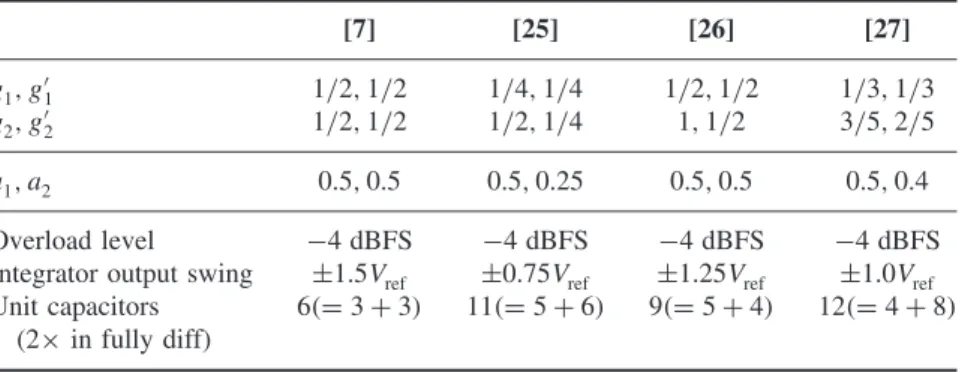
Generally speaking, the selection of the scaling coefficients of amodulator involves solving several trade-offs between architectural-, circuit-, and technological-level aspects of the practical implementation, so that the optimum selection for a given application may not apply in a different scenario. For the sake of illustration, Table 1.1 shows several sets of weights reported for the second-order, single-bit M in Figure 1.14. All sets exhibit an overload level XOL≈ −4 dBFS (i.e., −4 dB below the full-scale amplitude Vref=/2). The required integrator output swing and the minimum number of unit capacitors are also included. Capacitor sharing between weights in the same integrator has been considered.
φ2 φ2 φ2 φ1 φ1 φ1 φ2 φ1 φ2 φ1 φ1 φ1 φ1 φ2 φ2 φ2 φ2 φ2 φ1 φ2 φ1 φ2 φ2 φ1 φ2 φ1 φ1 + + − − − + + − − + X CS CS CI1 CS2 CS1 CS2 Ts CS1 OTA1 OTA2 CI1 CI2 CI2 Vref+ Vref− Vref+ Vref− Y
Figure 1.16 Fully-differential SC implementation of a second-ordermodulator.
Table 1.1 Comparison of some sets of coefficients reported for the second-order single-bitM [7] [25] [26] [27] g1, g1 1/2,1/2 1/4,1/4 1/2,1/2 1/3,1/3 g2, g2 1/2,1/2 1/2,1/4 1,1/2 3/5,2/5 a1, a2 0.5,0.5 0.5,0.25 0.5,0.5 0.5,0.4 Overload level −4 dBFS −4 dBFS −4 dBFS −4 dBFS Integrator output swing ±1.5Vref ±0.75Vref ±1.25Vref ±1.0Vref
Unit capacitors 6(=3+3) 11(=5+6) 9(=5+4) 12(=4+8)
(2×in fully diff)
Second-OrderM with Unity STF
Figure 1.17 shows an alternative second-order M topology that makes use of feed-forward paths to implement a so-called unity STF [28, 29]. Under linear analysis, the modulator output in theZ-domain yields
z−1 1 – z−1 z−1 1 – z−1 X1 X2 2 DAC ADC X Y
Figure 1.17 Second-ordermodulator with unity STF.
so that STF(z)=1—that is, the signal transfer function equals 1 at all frequencies—whereas NTF is unaffected.
One of the most appealing features of the unity-STFM in Figure 1.17 is that ideally there is no input signal trace processed by the integrators. Indeed, the integrator inputs in Z-domain can be obtained as
X1(z)= −(1−z−1)2E(z)
X2(z)=z−1(1−z−1)2E(z) (1.30)
showing that they depend only on the quantization error. In practice, there will be some residual component of the modulator input signal at the integrator inputs, but it is nor-mally negligible. This means that, if nonlinearities of the circuit implementation are accounted for, the generated distortion will be considerably lower for the unity-STF M in Figure 1.17 compared to the one traditionalM in Figure 1.14. Moreover, the technique is effective for any OSR, which makes unity-STFMs especially suited for lowering the sensitivity to circuit imperfections in wideband applications, in which low OSR values are required.
The described concept of unity STF can be extended to a noise shaping of any order. The only requirement is to ideally make STF(z)=1, without changing the modulator NTF. In recent years, it has been often applied in Ms for wideband and multimode applications [30–34].
1.4.2 High-Order
Ms
The simplest way to extend aM to an arbitraryLth-order shaping consists of including Lintegrators before the quantizer. Extending the second-orderM in Figure 1.14a, the topology in Figure 1.18 is obtained, which is known as an Lth-order single-loopM with distributed feedback [35].3 Ideally, its NTF can be derived from linear analysis
3The discrete-time filters H (z) in Figure 1.18 are assumed to be integrators with the transfer function in
a1 a2 aL
X H(z) H(z) H(z) ADC Y
DAC
Figure 1.18 High-order single-loopM with distributed feedback.
and equated to Equation 1.10 to derive a set of relations between the integrator scaling coefficients to be fulfilled for obtaining a pure-differentiator noise shaping—similarly as done in Equation 1.26 for the second-order M. The in-band quantization noise and the modulator DR would thus be ideally given by Equations 1.12 and 1.13, respectively. However, this modulator performance cannot be met in practice because Ms with pure-differentiator FIR NTFs are prone to instability ifL >2, exhibiting unbounded states and poor SNR compared to that predicted by linear analysis. In general, instability appears at the modulator output as a large-amplitude, low-frequency oscillation, leading to long bitstreams of alternating +1s and −1s. This tendency to instability can be explained as follows [36]. For aM to be stable, the quantizer input must not be allowed to become too large. As the quantizer input is obtained as (Figure 1.18)
Q(z)=STF(z)X(z)+[NTF(z)−1]E(z) (1.31)
the gain of NTF(z)−1, or simply NTF(z), must not be too large. However, as clearly visible from Figure 1.12, the out-of-band gain of FIR NTFs of the form(1−z−1)Lrapidly increases forL >2, yielding max[|NTF(f )|2]=22L
atf =fs/2. Consequently, it starts to overload the quantizer, which yields a significant decrease of the modulator SNR.
This problem can be circumvented by resorting to single-loop Ms with IIR NTFs of the form NTF(z)=(z−1)L/D(z), with D(z)being a polynomial determined by the modulator scaling coefficients that helps to limit the out-of-band gain of NTF.4However, unlike second-orderMs, for which a stability condition has been extracted [24], deter-mining exact conditions that guarantee the stability of higher-order, single-loopMs is still an open question. In [8, 37], it is shown, using behavioral simulations, that high-order Ms areconditionallystable; that is, with proper selection of the scaling coefficients, a stable operation can be obtained for inputs restricted within a certain range and for certain initial conditions of the state variables. However, despite the absence of general stability conditions, high-order Ms have been successfully designed since the late 1980s [38]. Indeed, the topology in Figure 1.18 has been widely used and optimal coefficients for it have been presented in [8].
4Note that the scaling coefficients can be thus designed to build a high-pass Butterworth or Chebyshev filter
Its STF and NTF can be calculated under linear analysis as5 STF(z)= kq L i=1aiH L (z) 1+kqLi=1 Lj=iaj HL−i+1(z) (1.33) NTF(z)= 1 1+kqLi=1 L j=iaj HL−i+1(z) (1.34)
If integrators described by Equation 1.16 are used as filters—H (z)=ITF(z)—the NTF can be approximated for low frequencies to [8]
|NTF| ≈ |1−z −1|L
kq Li=1ai (1.35)
in which the complete scaling of the outermost feedback branch of theM dominates the noise-shaping behavior. Similarly as done in Equations 1.11 and 1.12, the IBN of an Lth-order, single-loopM with distributed feedback thus yields
IBNL≈ 2 12 1 (kq Li=1ai)2 π2L (2L+1)OSR2L+1 (1.36)
so that the IBN increases by a factor 1/(kq Li=1ai)2 compared to an idealM. A major drawback of this loop filter implementation in Figure 1.18 is that the integrator outputs contain a significant amount of the input signal [41], so that the integrators require significant swing capabilities and/or the scaling coefficients need to be low. This can be circumvented using the loop filter topology in Figure 1.19, which is a chain of integrators withfeed-forward summation[42]. Under linear analysis, the corresponding STF and NTF can be calculated as STF(z)= kq L i=1aL−i+1HL−i+1(z) 1+kqLi=1aL−i+1HL−i+1(z) (1.37) NTF(z)= 1 1+kqLi=1aL−i+1HL−i+1(z) (1.38)
5The quantizer gain k
q of the linear quantizer model is explicitly considered hereinafter. As discussed in
Section 1.1.2, the gain of a multibit quantizer is clearly defined—for example,kq=1 if its input and output full-scale ranges are the same (Figure 1.4)—but that of a single-bit quantizer can be arbitrarily chosen. Neverthe-less, the effective value ofkqneeds to be estimated to quantitatively analyze the performance ofMs. Many different approaches exist to find a good approximation [8, 39, 40]. Among them, the one adopted here for the case ofMs with distributed feedback corresponds to that in [20]
kq= ⎧ ⎪ ⎨ ⎪ ⎩ 1/a1, single-bit first-order M 2/aL, single-bitLth-order M 1, multibit M (1.32)
X H(z) H(z) H(z) a2 aL a1 Y ADC DAC
Figure 1.19 High-order single-loopM with feed-forward summation.
H(z) H(z) H(z) a1 a2 ADC DAC b2 aL bL b1 X Y
Figure 1.20 High-order single-loopM with distributed feedback and distributed feed-forward input paths.
Note that NTF structure is the same as in Equation 1.34; therefore, the IBN of thisM topology yields an expression similar to that in Equation 1.36.
However, for the case of the distributed feedback topology in Figure 1.18 and the feed-forward summation topology in Figure 1.19, the loop filter for the STF and the NTF are essentially identical—compare Equation 1.33 with 1.34 and Equation 1.37 with 1.38. This means that, if the NTF is designed for the desired noise-shaping behavior, both topologies also fix the STF function, as STF(z)=1−NTF(z) [41].6
If a certain degree of freedom is desired in designing both the modulator NTF and STF, the topology in Figure 1.20 can be used, which is a chain of integrators with distributed feedback and distributed feed-forward input paths [43]. In this architecture, the zeros of STF can be fixed with coefficients bi without affecting
6In addition, the STF of the feed-forward summation architecture contains some peaking at high frequencies, what
the pole placement, so both STF and NTF can be separately optimized to some extent [41].7
1.5
Cascade
Modulators
As discussed in Section 1.4.2, stability problems arising from implementing a high-order NTF with a single-loop M can be circumvented with adequate scaling coefficients, but they result in a significant decrease of the DR compared with an ideal M. An alternative approach to obtain a high-order noise shaping while avoiding instabilities is found in the so-calledcascade Ms, also known as multiloopMs ormultistage noise shaping(MASH)Ms [45–48]. Their architecture is illustrated in Figure 1.21 and consists ofN stages ofmodulators, in which each stage remodulates a scaled version
ΣΔM1 (L1, B1) ΣΔM2 (L2, B2) ΣΔMN (LN, BN) HN(z) ADCN DACN X H1(z) H2(z) Hd1(z) Hd2(z) HdN(z) ADC1 DAC1 ADC2 Y DAC2 x1 e1 x2 q2 y2 c1 e2 c2 xN qN yN q1 y1 Digital Cancelation Logic
Figure 1.21 General topology of anN-stage cascademodulator.
7Local feedback loops—similar to those described in Section 1.7.2 for creating the notches in the NTF of BP
Ms—can also be included in LPM topologies above to move the NTF zeros away from DC and optimally spread them over the signal band to minimize the IBN [44]. NTFs with inverse Chebyshev filtering characteristics can also be designed [41].
of the quantization error generated in the preceding one. The outputs of the cascaded stages yiare conveniently processed in digital domain to cancel out at the overallM output yall the quantization errors, but that of the back-end stage. In addition, the latter quantization error appears at the cascade output shaped with an order L equal to the summation of those of the cascaded stages (L=L1+L2+ · · · +LN). Unconditionally, stable high-order shaping can thus be obtained if only first- and second-order Ms are cascaded (Li≤2), because all feedback loops are local to the low-order stages and there is no interstage feedback. Therefore, the performance of a multistage M is similar to that of an ideal high-order, single-loop with no stability issues.8
The operation principle of cascade Ms can be easily understood considering an exemplary two-stage cascade. Using linear analysis, the stages output can be expressed in theZ-domain as
Y1(z)=STF1(z)X1(z)+NTF1(z)E1(z)
Y2(z)=STF2(z)X2(z)+NTF2(z)E2(z) (1.39)
where the input of the stages are given by X1(z)=X(z) and X2(z)= −c1E1(z), andE1(z)andE2(z) stand for the quantization error of the respective stage. The overall modulator output after the digital cancelation logic (DCL) can thus be obtained from the expressions above as
Y (z)=Hd1(z)Y1(z)+Hd2(z)Y2(z)
=STFcasc(z)X(z)+NTF1,casc(z)E1(z)+NTF2,casc(z)E2(z) (1.40) where STFcasc(z), NTF1,casc(z), and NTF2,casc(z) stand for the overall cascade transfer functions for the input signal and the quantization errors, respectively
STFcasc(z)=Hd1(z)STF1(z)
NTF1,casc(z)=Hd1(z)NTF1(z)−c1Hd2(z)STF2(z) NTF2,casc(z)=Hd2(z)NTF2(z)
(1.41)
Note that, if the signal processing in the DCL matches part of the signal processing in the analog side, Equation 1.41 yields
Hd1(z)=STF2(z) Hd2(z)= c1 1NTF1(z) ⇒ ⎧ ⎪ ⎨ ⎪ ⎩ STFcasc(z)=STF1(z)STF2(z) NTF1,casc(z)=0 NTF2,casc(z)= c1 1NTF1(z)NTF2(z) (1.42)
so that the first-stage quantization error is canceled at the overall output and that of the second stage is attenuated with an order equal to the summation of both stages’ orders (L=L1+L2).
8CascadeMs can beideallyextended to an arbitrary number of stages. However, as will be shown in detail
in Chapter 2, the effectiveness of cascading a large number ofstages to achieve an arbitrary high-order noise shaping is limited in practice by circuit nonidealities, which preclude the complete cancelation of low-order-shaped quantization errors of the front-endstages at the modulator output. This effect is known asnoise leakage.
For the generic N-stage cascadeM in Figure 1.21, assuming STFi(z)=z−Li and NTFi(z)=(1−z−1)Li in the individual stages, the overall modulator output thus yields
Y (z)=z−LX(z)+ N1−1 i=1 ci (1−z−1)LEN(z), with L= N i=1 Li (1.43)
under the required matching between the analog processing in the stages and the DCL. The in-band quantization noise of the cascade is then given by
IBNcasc= 2 N 12 1 N−1 i=1 ci2 π2L (2L+1)OSR2L+1 (1.44)
where N stands for the quantization step employed in the last stage. Note from Equation 1.44 that only the interstage scaling coefficients ci, which prevent a premature overload of the subsequent stages, decrease the performance below that of an ideal Lth order M. Typical values of 1/ Ni=−11ci are between 2 and 4 if single-bit quantization is employed, which lead to a reduction in the ideally attainable DR of only 6–12 dB (1–2 bit). These performance losses are inherent to cascadeMs, but they are significantly smaller than those resulting from optimized high-order single loops. In addition, they are independent of OSR.
The aforementioned benefits of cascadeMs have favored the development of a large number of different topologies:
• 2-1M, which stands for a third-order two-stageM built up with a second-order stage followed by a first-order one [46]. It is also known as a SOFO cascade—for second-order first-order.
• 2-2 M, which represents a fourth-order cascade built up with two second-order stages [49, 50].
• 2-1-1 M, which stands for a fourth-order, third-stage cascade [25].
• 2-2-1 M [51].
• 2-1-1-1M [52].
• 2-2-2 M [53].
• etc.
Note from the cascade topologies above that the first stage is usually a second-order M and that first-order Ms are avoided at the front end [48]. The reason for that is twofold. First, the quantization error from the first stage would be only first-order shaped and noise leakages would be larger. Second, the tonal behavior of a first-order, first stage would menace the performance of the cascade. In addition, although low-orderstages are most frequently cascaded, 3-1 and 3-2Ms have also been reported [54, 55].
Figure 1.22 illustrates the block diagram of a 2-1-1 cascade, in which coefficients ai represent the in-loop integrator scaling factors, whereas coefficients bi and ci determine the interstage scaling factors. The first stage performs as an ideal second-orderM and
X a1 a2 b1 c1 a3 a4 b2 c2 Y1 Y z−1 1 – z−1 z−1 1 – z−1 z−1 1 – z−1 z−1 1 – z−1 ADC1 1/(a1a2) Hd2(z) Hd3(z) 1/a3 DAC1 DAC2 DAC3 ADC2 ADC3 Hd1(z)
Figure 1.22 Block diagram of a 2-1-1 cascade modulator using the notation in [8, 9]. The relations in Equations 1.45 and 1.46 must be fulfilled for the correct operation of the cascade.
the second and third stages as an ideal first-orderM under the assumptions kq1a1a2=1, kq1a2=2
kq2a3 =1 kq3a4 =1
(1.45)
wherekqi stands for the gain of the quantizer in theithstage. The matching required between the signal processing in the stages and the digital processing in the DCL leads to Hd1(z)=z−2[1+(b1−1)(1−z−1)2][1+(b2−1)(1−z−1)3] Hd2(z)= 1 c1z −1 (1−z−1)2[1+(b2−1)(1−z−1)3] Hd3(z)= 1 c1c2(1−z −1)3 (1.46)
X g1 Y1 Y2 Y3 Y g2 g3 g'2 g''3 g'3 g'4 g''4 g4 g1=g'1 Hd1(z) Hd2(z) Hd3(z) g'1 z−1 1 – z−1 z−1 1 – z−1 z−1 1 – z−1 z−1 1 – z−1 ADC1 ADC2 DAC1 DAC2 ADC3 DAC3
Figure 1.23 Alternative representation of the 2-1-1 M in Figure 1.22 using the notation in [12, 19]. Modulator coefficients(ai, bi, ci)are mapped onto integrator input coefficients(gi, gi, gi), which are closer to the circuit-level implementation.
for a complete cancelation of the first- and second-stage quantization errors at the cascade output. For the sake of completeness, Figure 1.23 shows an alternative representation of the 2-1-1 M according to the notation in [12, 19]. Proceeding in a similar way as done in Figure 1.15 for the second-order M, both notations can be easily connected with the equalities:
a1 = g 1g2 g2 , a2 =g 2, a3=g 3, a4=g 4 b1 = g 3 g1g2g3, b2 = g4 g3g4 c1= g 1g2g3 g3 , c2= g3g4 g4 (1.47)
Table 1.2 Comparison of some sets of coefficients reported for the 2-1-1 single-bitM [56] [25] [27] g1, g1 1/4,1/4 1/4,1/4 1/3,1/3 g2, g2 1,1/2 1/2,1/4 3/5,2/5 g3, g3, g3 1,1/2,1/2 1,3/8,2/8 5/6,3/6,2/6 g4, g4, g4 1,1/2,1/2 1,1/4,1/4 1,1/3,1/3 a1, a2, a3, a4 0.5,0.5,0.5,0.5 0.5,0.25,0.25,0.25 0.5,0.4,0.33,0.33 b1, c1, b2, c2 2,0.5,1,1 3,0.5,1,1 3,0.5,1,1 1/(c1c2) 2 2 2 Loss of DR −6 dB −6 dB −6 dB Overload level −3 dBFS −2.5 dBFS −2 dBFS Integrator output swing ±(0.75,1,1,1)Vref ±(0.75,0.7,0.6,0.6)Vref ±(1,1,0.9,0.8)Vref
Unit capacitors (2×) 17(=5+4+4+4) 35(=5+6+16+8) 29(=4+8+11+6) The value of the analog coefficients in the 2-1-1 M need to be selected to fulfill the relations in Equation 1.45, but many different sets of values can do the work. On top of that, extra considerations are in practice taken into account, such as the following: • Minimizing the resulting loss of performance in comparison to an idealM. • Maximizing the modulator overload level to achieve a high-peak SNR.
• Simplifying the circuit-level implementation of the set of analog coefficients. For Ms, this means taking into account practical capacitor ratios using unit elements, enabling capacitor sharing within the integrators, reducing the total number of unit capacitors for area saving, etc.
• Minimizing the integrator output swing requirements, especially in case of a low-voltage supply.
• Simplifying the implementation of the DCL. To that purpose, power of two coefficients are often preferred forb1,b2, 1/c1, and 1/c2—see Equation 1.46 —in order to use shift registers only.
Table 1.2 illustrates some sets of analog coefficients reported for the 2-1-1 single-bit M, together with their main resulting features. Optimized coefficients for some other cascade topologies can be found in [8].
1.6
Multibit
Modulators
As discussed in Section 1.2.4, the DR of a M can be enhanced if the resolution of the embedded quantizer is increased. The main advantages of resorting to multibit modulators are as follows:
• The in-band quantization noise power is roughly reduced 6 dB per additional bit in the embedded quantizer, thanks to the smaller quantization step.
• Internal nonlinearities are weaker in multibitMs than in their single-bit counterparts. The quantizer operation better fits the additive white noise model in Section 1.1.3 and the phenomena caused by nonlinear dynamics are less evident.
• For a given order in the loop filter, the stability properties of multibit Ms are better than for single-bit Ms [57].
These benefits suggest that, for a targeted performance of the M, multibit quanti-zation can be traded for noise shaping and/or oversampling. Indeed, multibitMs are often employed in broadband applications to compensate for the limited OSR. Never-theless, multibit quantizers also have important drawbacks that may counter the former advantages:
• They require more analog circuitry and are more difficult to design than single-bit ones. • Contrary to 1-bit quantizers, which are intrinsicallylinear because only two levels are used for quantization, multibit quantizers exhibit in practice some nonlinearities in their transfer characteristic, mostly due to devicemismatching, which significantly influence theM performance.
1.6.1 Influence of Multibit DAC Errors
Figure 1.24 illustrates an enhanced version of the linear model of a multibit M in Figure 1.8b. Errors related to the multibit conversion are added to the quantization error ethat has been considered so far; namely, an erroreADCassociated to the A/D conversion and an error eDAC in the subsequent D/A conversion required to reconstruct the analog feedback signal. Note that eADC is injected in the same path as the quantization error e and, therefore, it is also attenuated within the signal band by noise shaping. However, DAC errors are injected in the feedback path and, therefore, they directly add to theM input signal and pass to theM output as part of the input signal itself. Consequently, the linearity of a multibitM will beno betterthan that of the multibit embedded DAC and the latter must be designed to achieve the linearity targeted for the wholeADC, what may be challenging under the influence of component mismatching.
Figure 1.25 conceptually illustrates the parallel architecture that is typically used for the multibit quantizer in Ms, in which the resolution is usually low (B ≤5). The B-bit ADC consists of a bank of 2B−1 comparators that digitizes the loop filter output into thermometer code, which will be subsequently coded into binary. The DAC employs 2B−1 unit elements (capacitors, resistors, current sources, etc., depending on the circuit
x(n) kq q(n) y(n) e(n) yDAC(n) eDAC(n) eADC(n) H(z)
q y y DAC M = 2B-1 U0 U1 UM-2 UM-1 2B-1 comparators 2B-1 elements B-bit DAC B-bit ADC ref0
Figure 1.25 Parallel topology of a typical multibit quantizer embedded in aM.
implementation) to reconstruct the analog feedback signal using 2B levels (numbered from 0 to M=2B−1). The ith analog output level is generated by activating i unit elements and adding their outputs (charges or currents). DAC errors are caused by the mismatching between its unit elements, which makes the DAC output levels deviate from their nominal values. Assuming that the actual value of each unit element follows a Gaussian distribution, the worst-case relative error in the DAC output yDAC can be estimated as σ yDAC yDAC ≈ 1 2√2B σ U U (1.48) whereσ(U/U )stands for the relative error in the value of the unit element. Obviously, the DAC accuracy increases with the number of unit elements, thanks to the parallel topol-ogy. However, for a M with 4-bit embedded quantization to achieve 16-bit linearity, the required matching for the DAC unit elements should be better than 0.01% (13 bits). Device matching achieved in present-day CMOS processes is nevertheless in the range of 0.1% (10 bits) and the required accuracy in the elements can only be obtained through the parallel connection of many more of them (∼64). This means that achieving linearities better than 12 or 13 bits in multibitMs by means of relying only onstandarddevice matching usually leads to prohibitive area occupation.
A direct method to improve the standard device matching is laser trimming, what can sometimes be done at the foundry, but at the expense of additional fabrication and/or measurement steps and increased cost. Calibration and correction schemes have also been proposed, either in analog or digital domain [58], but they are often expensive to implement in terms of system design complexity, hardware requirements, and power consumption.
Among the different alternatives that have been developed through the years for achiev-ing high-linear multibitMs, two of them clearly prevail because of the modest com-ponent matching required and the reduced circuit complexity involved. These approaches are discussed in the following text.
1.6.2 DEM Techniques
As previously discussed, mismatches among the unit elements cause DAC nonlinearities that generate harmonic distortion in the