Printed in The Islamic Republic of Iran, 2015 © Shiraz University
“Research Note”
THREE PHASE ON-LINE UPS BY IMPLEMENTING T-SOURCE INVERTER
WITH MAXIMUM CONSTANT BOOST PWM CONTROL
*K.CHITRA
**AND A. JEEVANANDHAM
Dept.of EEE, Bannari Amman Institute of Technology, Sathyamangalam, Tamilnadu, India Email: [email protected]
Abstract– This paper presents the new topology of three phase on line Uninterruptible Power Supply (UPS) by employing T-Source Inverter (TSI) with maximum constant boost Pulse Width Modulation (PWM) control and the results are compared with the conventional Uninterruptible Power Supply (UPS). The conventional UPS consists of Voltage Source Inverter (VSI) with step up transformer or DC-DC booster which decreases the efficiency and increases energy conversion cost. The proposed three phase UPS with TSI has the voltage boost capability through shoot through zero state which is not present in the conventional VSI. This proposed UPS increases the efficiency due to single stage conversion, reduces the harmonics, increases the voltage gain and reduces the voltage stress. The performance of the three phase on-line UPS with TSI is simulated in MATLAB / SIMULINK software and the results are compared with conventional UPS. The simulation and the theoretical analysis are validated with experimental results.
Keywords– On-line UPS, T-Source Inverter, maximum constant boost, boost factor
1. INTRODUCTION
The purpose of implementing uninterruptible power supply (UPS) is to provide clean and uninterrupted
high quality power to sensitive loads like life supporting systems, medical instruments, communication systems, data centers, industrial control units and computers [1-3]. Regardless of quality of the AC input, UPS system provides uninterrupted, reliable, distortion free, high quality power [4]. There are two types
of conventional UPS. The first type of UPS consists of rectifier, battery, inverter and step up transformer [5]. The second type of UPS consists of rectifier, battery, DC-DC booster and inverter [6-8]. The control of switches in the booster circuit is complicated, efficiency is decreased and cost is increased due to the
equipment used for increasing the voltage. Conventional VSI can only buck the input voltage. In VSI, the switches in the same lag are not switched on simultaneously, hence to avoid shoot through the dead time is introduced which leads to waveform distortion [9].
Professor Zhi Jian Zhou in 2008 [10] proposed Z-source inverter for the single phase UPS. This method offers the following advantages: 1) buck- boost operation 2) step up transformer and dc-dc booster is not required 3) output voltage distortion is less. But in ZSI the voltage stress in the switches is high and
more L&C components are used. These drawbacks are eliminated in TSI. In this paper a new topology of UPS is proposed using T-Source inverter with maximum constant boost PWM control. The proposed UPS offers the following advantages: 1) Buck and boost operation 2) Less THD 3) Voltage stress is minimized
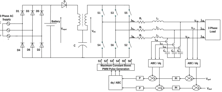
4) Fewer Components 5) High efficiency. The overall circuit diagram for the three phase on-line UPS with T-Source inverter is shown in Fig. 1.
Received by the editors February 11, 2014; Accepted August 4, 2015.
S1 S4 S3 S6 S5 S2 3 Phase Load Vinput D C VDC AC AC AC
3 Phase AC Supply
D1
ABC / dq ABC / dq
D3 D5
D4 D6 D2
Rl
Rl
Rl
Cl Cl Cl
VCR Ll Ll VCY VCB Ll ICR ICY ICB PI PI P P dq / ABC
Maximum Constant Boost PWM Pulse Generation
S1 S2 S3 S4 S5 S6
Vqref Vdref + + + + _ _ _ _ IIR IIY IIB ILR ILY ILB Battery
Fig. 1. T-source inverter for the proposed UPS
2. MODELING OF TSI CIRCUIT
DC-DC input stage in boost type voltage source inverter is replaced by ‘X’ shape LC network in ZSI [11-12]. To reduce the number of LC components, the coupled inductors are designed on a common magnetic core [13]. In TSI high frequency low leakage inductance transformer and one capacitor is used instead of LC lattice in ZSI, which is shown in Fig. 1.
a) Operating modes of TSI
T-Source inverter utilizes the shoot through zero state to boost the output voltage. During shoot through state, switches in the same leg are turned on simultaneously. TSI can be operated in two operating modes, namely active mode and shoot through mode [13]. Active mode is also called non shoot through mode. During active mode the input voltage appears across the capacitor and the diode is forward biased and conducts. During shoot through mode the output voltage is boosted and the inductor limits the current ripple and the voltage across the load is zero. The TSI equivalent circuits during shoot through mode and active mode are shown in Fig. 2a and 2b.
DC
Vinput
C L
(Vc-Vinput)/n
Vout=VDC
Iout
.
Vc Iin L DC Vinput N.VC C VcVout=0
Iout
.
Vc.
Iin.
Vc-Vinput
(a) (b)
Fig. 2. T-Source inverter in (a) Shoot through (Tshoot) state (b) active (Tactive) state
b) Boost factor and voltage stress of TSI
Tshoot : Shoot through time period
Tactive : Active time period
For the switching period Ts the average voltage across the transformer inductances is zero [13].
-
0VL TshootVCTactive Vinput VC n T
(2)
The capacitor voltage and output voltage are functions of shoot through duty ratio d.
s
d
T
shoot
T
(3)
1
.
1
1
1 .
;
1
input
V
C
V
T
active
T
active
n T
shoot
d
n
d
d
n
(4)The maximum value of d for TSI with n > 1 is smaller than the ZSI. Hence the same output voltage can be obtained with smaller shoot through time period [13].
Using (5), VDC during non shoot through state can be obtained.
/ 1
1 .
DC C C input input
V
V
V
V
n V
n
d
(5)By substituting (4) into (5)
s
DC input input
active shoot
T
V V BV
T T
(6)
where
1
1 2 s
shoot
active shoot
s
T B
T
T T
T
(7)
The output peak voltage of the inverter is given by,
= M.B.V
ac dc input
V M V (8)
From (8), the voltage gain of the T-Source inverter can be expressed as
ac
input
V
G
MB
V
(9)Thus, any desired output voltage can be obtained by properly selecting the boost factor (B) and the modulation index (M) regardless of the battery bank voltage.
The voltage stress Vstress across the switches in TSI can be expressed as [14-16]
stress input
V BV (10)
3. MAXIMUM CONSTANT BOOST PWM CONTROL
In this paper maximum constant boost control method is used for the TSI, which gives the maximum voltage gain by keeping the shoot through duty ratio constant. The shoot through duty ratio is maintained as constant in order to reduce the cost and volume [17-18]. To reduce the voltage stress across the switches a great voltage boost is desired for any modulation index. The reference signals VR, VY, VB which
produced by two shoot through envelope signals Vpos and Vneg. The inverter is in shoot through state when
the carrier wave is greater than the upper shoot through envelope Vpos (Vtri > Vpos) or the carrier wave is
lower than the lower shoot through envelope Vneg (Vtri < Vneg) [17]. The signals Vpos and Vneg are
periodical curves and the frequency is three times the output frequency. The shoot through duty ratio should be the same for the switching cycle in order to maintain a constant boost, because the boost factor depends on shoot through duty ratio (d). This proposed control method provides the maximum constant boost and minimizes the voltage stress.
4. CLOSED LOOP CONTROLLER FOR PROPOSED UPS
Closed loop controller is designed to achieve distortion free output voltage, voltage tracking and disturbance rejection [19-20]. In the proposed UPS system shown in Fig. 1, the output ac voltage is controlled by varying the modulation index M. The voltage and current equations for inverter ac side is obtained using Kirchoff’s voltage law and current law for each phase.
There are two control loops in the proposed UPS. They are inner current control loop and outer voltage control loop [20]. Capacitor current measurement is taken as the feedback current and load current is taken as disturbance current. The proportional controller is included to obtain the desired bandwidth. The outer voltage control loop is used to achieve proper voltage tracking. PI controller which is connected in series is to remove the steady state error and to get good reference tracking and disturbance rejection [21].
5. RESULTS AND DISCUSSION
The proposed TSI for 3 phase on line UPS with maximum constant boost control technique was simulated using MATLAB/simulink software. Twenty 12 V lead acid batteries are connected in series in this UPS, so the input battery bank voltage is 240 V. The operating parameters given in Table 1 were chosen for the simulation of the proposed UPS.
Table 1. Operating Parameters of the proposed UPS
Parameter Value
Input DC voltage 240 V
T-Source inductance 0.01 mH
T-Source capacitance 48 μF
Switching frequency 5 kHz
Power factor 0.8
Load 5 kW
Boost factor 1.8
Modulation index 0.8
0 .01 .02 -40
-20 0 20 40
Time (Sec)
V
o
lt
a
g
e
M
a
g
n
it
u
d
e
Maximum Constant Boost Pulse Generation Vpos
Vneg
VR VY VB Carrier Signal Vtri
Fig. 3. Maximum constant boost control and Switching Pulses
-500 0
500 Output Phase Voltage with Filter
0 .05 .1 .15 .2
-500 0
500 Vc (Volts)
Time (Sec)
-500 0
500 Vb (Volts)
-500 0
500 Va (Volts)
-20 0
20 Output Phase Current with Filter (A)
-20 0
20 Ia (A)
-20 0
20 Ib (A)
0 .05 .1 .15 .2
-20 0 20
Time (Sec) Ic (A)
(a) (b)
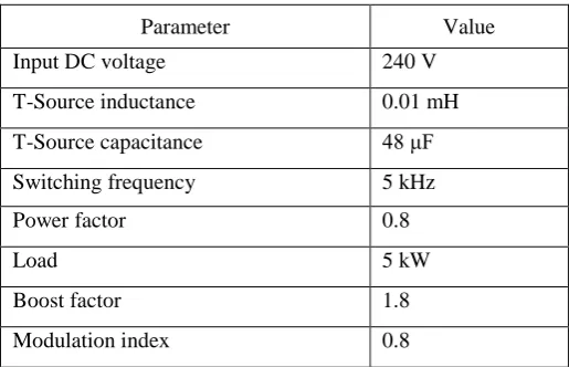
Fig. 4. (a) Output Phase Voltage (Peak-Peak) (b) Output Phase Current (Peak-Peak)
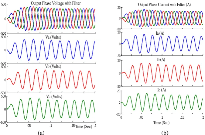
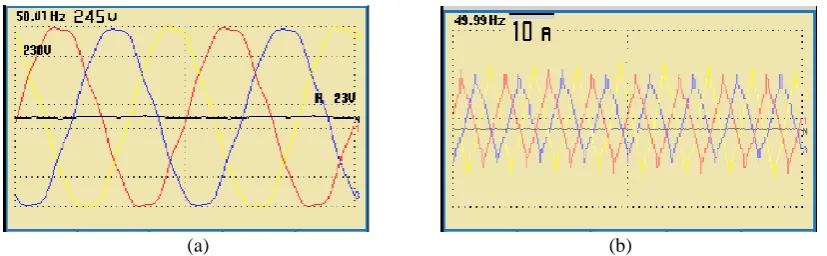
Fig. 5. (a) Experimental setup of the proposed UPS (b) Output voltage THD comparison
(a) (b)
Fig. 6. Experimental waveforms of (a) output RMS phase voltage (b) Output RMS phase current
The proposed UPS is efficient when compared to the traditional UPS because of its single stage conversion and fewer components. From the Fig. 5b it is evident that the output voltage THD of proposed UPS with TSI is less than the traditional UPS. This increases the power quality of the proposed UPS.
6. CONCLUSION
In this paper, a new topology of three phase on-line UPS with TSI has been presented. The simulation of the proposed UPS is carried out for different loading conditions and the results are validated with experimental results. The comparison of proposed UPS with TSI is done based on power quality, efficiency and cost efficiency with the traditional UPS based on step up transformer, dc-dc booster and ZSI. The output voltage THD and current THD of the proposed UPS are less than the traditional UPS. The conduction losses in the switches and also the voltage stress are reduced in this proposed UPS. The efficiency of the proposed UPS with T-Source inverter based on maximum constant boost control is higher than the traditional UPS.
REFERENCES
1. Emadi, A., Nasiri, A. & Bekiarov, S. B. (2005). Uninterruptible power supplies and active filters. CRC Press.
2. Racine, M. S., Parham, J. D. & Rashid, M. H. (2005). An overview of uninterruptible power supplies. Annual
North American 2005 Power Symposium; 23–25, pp. 159–164.
3. Guerrero, J. M., Garcia de Vicuna, L. & Uceda, J. (2007). Uninterruptible power supply systems provide
protection. IEEE Industrial Electronics, Vol. 01, pp. 28–38.
4. Ashrafi, B., Niroomand, M. & Ashrafi Nia, B. (2012). Novel reduced parts on-line uninterruptible power supply.
5. Jain, P. K., Espinoza, J. R. & Jin, H. (1998). Performance of a single-stage UPS system for single-phase
trapezoidal shaped AC voltage supplies. IEEE Trans Power Electron, Vol. 13, pp. 912–923.
6. Brancol, C. G. C., Cruz, C. M. T., Torrico Bascope, R. P., Antunes, F. L. M. & Barreto, L. H. S. C. (2006). A
transformerless single phase on line UPS with 110V/220V input output voltage. IEEE 2006 Applied Power
Electronics Conference, pp. 348–354.
7. Park, J. K., Kwon, J. M., Kim, E. H. & Kwon, B. H. (2008). High performance transformer less online UPS.
IEEE Trans Ind Electron, Vol. 55, 2943-2953.
8. Lai, C. H. & Tzou, Y. Y. (2002). DSP embedded UPS controller for high performance single phase on line UPS
systems. IEEE 2002 Industrial Electronics Conference, pp. 268–273.
9. Kawamura, R. & Chuarayapratip Haneysoshi, T. (1988). Deadbeat control of PWM inverter with modified pulse
patterns for uninterruptible power supply. IEEE Trans Ind Electron, Vol. 35, pp. 295–300.
10. Zhou, Z. J., Zhang, X., Xu, P. & Shen, W. X. (2008). Single-phase uninterruptible power supply based on
Z-source inverter. IEEE Trans Ind Electron, Vol. 55, pp. 2997–3004.
11. Peng, F. Z. (2003). Z-source inverter. IEEE Trans Ind Appl, Vol. 39, pp. 504–510.
12. Peng, F. Z. (2008). Z-source networks for power conversion. IEEE Applied Power Electronics Conference, pp.
1258-1265.
13. Strzelecki, R., Adamowicz, M., Strzelecka, N. & Bury, B. (2009). New type T-Source inverter. IEEE Power
Electronics Conference, pp. 191-195.
14. Qian, W. & Peng, F. Z. (2011). Trans-Z-Source Inverters. IEEE Trans Power Electronics, Vol. 26, pp.
3453-3463.
15. Ding, L. I., Chiang Loh, P., Zhu, M. (2013). Cascaded multicell Trans-Z-source inverters. IEEE Trans Power
Electronics, Vol. 28, pp. 826-836.
16. Shen, M., Joseph, A., Peng, F. Z., Leon, M. & Adams, D. J. (2006). Constant boost control of the Z-source
inverter to minimize current ripple and voltage stress. IEEE Trans Ind Appl., Vol. 42, pp. 770-778.
17. Peng, F. Z., Shen, M. & Qian, Z. (2005). Maximum boost control of the Z-source inverter. IEEE Trans Power
Electron, Vol. 20, pp. 833–838.
18. Loh, P. H., Vilathgamuwa, D. M., Lai, Y. S., Chua, G. T. & Li, Y. W. (2005). Pulse width modulation of
Z-source inverters. IEEE Trans Power Electron, Vol. 20, pp. 1346-1355.
19. Tran, Q. V. & Chun, T. W. (2007). Algorithms for controlling both the DC boost and AC output voltage of
Z-source inverter. IEEE Trans Ind Electron, Vol. 54, pp. 2745-2750.
20. Gajanayake, C. J., Vilathgamuwa, D. M. & Loh, P. C. (2006). Modeling and design of multi-loop closed loop
controller for Z-source inverter for distributed generation. IEEE Power Electronics Conference, pp. 1353–1359.
21. Hasanzadeh, A. & Mokhtari, H. (2009). A simplified droop method implementation in parallel UPS inverters
with proportional-resonant controller. Iranian Journal of Science and Technology, Transactions of Electrical