Iranian Journal of Electrical and Electronic Engineering, Vol. 15, No. 2, June 2019 172
An Intelligent Non-Trial-and-Error Design Method for
Double Screen Frequency Selective Surfaces
H. Rajabalipanah*
(C.A.), M. Fallah** and A. Abdolali*
Abstract: An intelligent design method of double screen frequency selective surfaces (FSSs) is addressed in this paper. The employed unit cell is composed of two metallic screens, which are printed on both sides of a substrate. The presented non-trial-and-error approach is investigated based on the separate design of each screen. With the help of some physical intuition and an equivalent circuit model, it is shown that the conventional use of complement geometries restricts the final desired filtering response. Therefore, unlike the previous studies, the metallic screens are not geometrically complementary in this paper. An excellent agreement between the full-wave simulations and corresponding equivalent circuit models has been observed. Using standard lumped elements, a highly selective miniaturized FSS (0.06λ0 ~ 0.08λ0) with two closely-spaced pass bands is designed, for
GSM and WLAN frequencies. Simulation results show a dual-polarized characteristic with a good angular stability performance for the proposed structure.
Keywords: Frequency Selective Surfaces, Filter, Dual Band, Equivalent Circuit Model.
1 Introduction1
REQUENCY Selective Surfaces, or FSSs in abbreviated form, are usually periodic metallo-dielectric patterns, which exhibit a certain frequency response to the incoming electromagnetic (EM) waves [1]. In recent years, due to flexible EM properties, these structures have attracted many applications such as filtering [2, 3], shielding [4-6], secure electromagnetic buildings [7], antenna engineering [8, 9], stealth [10-14], etc. According to performance when illuminated by EM waves, FSSs and metasurfaces with sub-wavelength elements are widely used in different frequency regions from microwave to visible regions [15-23]. Localized frequency-selective behavior, angle independent performance and low sensitivity to the neighboring elements make these structures an ideal choice for
Iranian Journal of Electrical and Electronic Engineering, 2019. Paper first received 29 March 2018 and accepted 05 October 2018. * The authors are with the Applied Electromagnetics Lab, Department of Electrical Engineering, Iran University of Science and Technology (IUST), Tehran, Iran.
E-mails: [email protected] and [email protected]. ** The author is with the Department of Electrical Engineering, Iran University of Science and Technology (IUST), Tehran, Iran. E-mail: [email protected].
Corresponding Author: H. Rajabalipanah.
various electromagnetic applications. Miniaturized FSSs are harmonic free, so their behavior can be evaluated by equivalent circuit models (ECMs) [24-26]. The miniaturized property of these FSSs avoids the disturbing effects such as grating lobes especially at high incident angles [1]. Nowadays several studies for the miniaturization of FSS have led to the structures with angular stable frequency responses [27-29]. However, due to the lack of appropriate symmetry, low quality factor (Q) and poor insertion losses for the presented pass/reject bands, their frequency responses do not have special applications [30, 31]. In addition, in other researches, despite the angular stability of the designed FSSs, because of the geometrical asymmetry, there is no stability against the different polarizations of the incident wave [32, 33]. Most of the mentioned references use a trial-and-error design method. These drawbacks pose a great limit in their applications. On the other hand, in most literature on the dual-band and even single-band FSSs, frequency-tuning capability of the proposed structures is not provided. In other words, it is not stated which parameters should be changed in what direction [33] to obtain new pass/reject bands. In other papers, frequency tuning of the proposed structures is investigated according to some of the geometric parameters, but there is little physical discussion of the effects of these parameters [15].
F
Iranian Journal of Electrical and Electronic Engineering, Vol. 15, No. 2, June 2019 173
In this paper, an intelligent non-trial-and-error design method for double screen FSSs is addressed based on separate optimization of each screen. The proposed unit cell is composed of two meandered metallic screens, which are printed on both sides of a substrate. A comprehensive parametric study has been conducted to evaluate the effects of the parameter variations. With the help of physical intuition and an equivalent circuit approach, it is found that the complement geometry of the metallic screens restricts the final desired filtering response. Therefore, unlike previous works, in this manuscript the presented metallic screens are not complementary from the aspect of geometric parameters. As a prototype of the proposed method, a novel miniaturized frequency selective surface (FSS) with two closely space transmission poles is designed for WLAN and GSM frequencies. The simulation results show a dual-polarized operation with an appropriate angular stability, which highlights the practical functionality of the proposed structure.
2 FSS Design and Analysis
The schematic of two employed FSS screens is depicted in Figs. 1(a) and 1(b) and the primary geometric parameters are given in Table 1. The geometry of the elements is chosen to be symmetric with respect to x- and y- axis to ensure independent performance of screens for both polarizations. The unit cell dimensions are chosen as 10.8 mm×10.8 mm (0.06λ0 ~ 0.08λ0) arbitrarily. Two meandered screens
are printed on both sides of a Rogers RT5880 substrate (εr = 2.2, tanδ = 0.0009) with a thickness of t = 1.575 mm. The transmission coefficient of the metallic strip screen has a first-order band reject and that of the aperture screen has a first-order band pass filtering response. The presented unit cell has two key differences from that in [15]. First, the geometric parameters of both of screens have been adopted fully independent of each other, which means that in general case w1≠w2, g1≠g2,… . Second, it will be shown that
assuming equal intervals for δi (i=1,2,3) in [15] will create a limitation for designing and adjusting the inductance and capacitance values of the screens. Hence, these intervals are chosen different from each other in this paper.
In [15], in which two complementary screens are used, the effect of some geometric parameters on the resultant frequency response is reviewed. However, since both of the screens are geometrically complementary, there is not complete control of the frequency response of optimized structure. As a result, in this manuscript, the geometric parameters of two screens are not linked together. The design method of the frequency response is different in this paper in such a way that by separate design of the frequency responses of each screen, the filtering characteristics of the final structure can be tuned. This method allows us to have a full control of the center frequencies and the
(a)
(b)
Fig. 1 The schematic of presented unit cell of a) Metallic strip screen and b) Aperture screen.
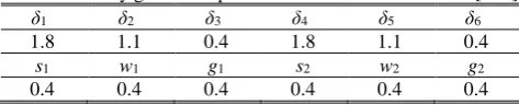
Table 1 Primary geometric parameters of both of screens in [mm].
δ1 δ2 δ3 δ4 δ5 δ6
1.8 1.1 0.4 1.8 1.1 0.4
s1 w1 g1 s2 w2 g2
0.4 0.4 0.4 0.4 0.4 0.4
quality factors (Q) of the pass bands, which play a vital role in the applicability of frequency selective surfaces. For optimal tuning of the final frequency response, it is shown that a collection of geometric parameters (not one parameter) in certain directions should be changed. In the following, a comprehensive parametric study for each of metallic screen is conducted and the corresponding filtering responses are discussed.
2.1 Filtering Characteristic of Each Screen
The filtering specifications of each screen is now investigated through the simulation results. According to the goal of this paper, it is assumed that the frequency response of a screen should not influence the other one. All of the relationships and enforced arguments in this study are based on this issue. On the other hand, as it is well known, in a substrate by increasing the relative permittivity (εr) , the electric field lines are more
concentrated in the dielectric. Thus, the aforementioned effects of the screens on each other will be more accurate when the substrate has a low relative permittivity (εr) [3]. As a result, a substrate with low
Iranian Journal of Electrical and Electronic Engineering, Vol. 15, No. 2, June 2019 174
relative permittivity is used for the design in this manuscript. Considering the final second-order filter, which is composed of two first-order ones, to obtain the individual frequency response of each screen, the substrate thickness is considered as t = 0.787 mm (i.e. half of the second-order substrate thickness). The magnitude of transmission coefficients (S21) for each of screen obtained by full wave simulation (MOM) and equivalent circuit model (ECM) are depicted in Fig. 2. As can be seen, the full wave results are in a good agreement with those of equivalent circuit model. As it is shown in Fig. 2, the metallic strip screen has a first-order band-stop frequency response with a center frequency of 4.5 GHz and the aperture screen has a first-order band-pass response with a center frequency of 4.3 GHz. The corresponding ECMs are illustrated in Figs. 3(a) and 3(b). The metallic strip and aperture screens are modeled as series and parallel LC resonators, respectively. The employed substrate is also modeled as a transmission line with the characteristic impedance of Zc Z0 r in which Z0120 is the
characteristics impedance of free space. To obtain the values of inductance and capacitance, the unit cell of each screen has been simulated by Computer Simulation Technology (CST) software. Then, using a genetic algorithm, different values are assigned to the capacitance and inductance values in such a way that the full-wave and equivalent circuit model have a similar frequency responses.
2.2 Separate Tuning of Frequency Responses
Considering the presented ECMs in Figs. 3(a) and 3(b), it is obvious that in both structures, the center frequency decreases by increasing C, L. On the other hand, the quality factors of the metallic strip and
aperture screens are defined as QMS∝ L C/ and
QAP∝ C L/ , respectively. Thus, it can be seen that by
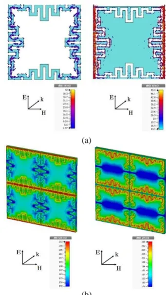
increasing L, the quality factor of the metallic strip screen increases while the quality factor of the aperture screen decreases. Also, by increasing C, the bandwidth of the metallic strip structure increases and the bandwidth of the aperture structure decreases. As a result, for an intelligent control of the filtering characteristics, it is required to know the geometric parameters effect on the inductance and the capacitance values in both of screens. It is known that the efficient path of the surface currents makes the inductance of screens and the capacitance is made by the existing air gaps as shown in Fig. 4. In the following, the physical effects of geometric parameters in the inductance and capacitance values of the employed unit cell is discussed. It should be noted that the mentioned discussion is given in detail for the metallic strip screen but just to avoid mentioning oft-repeated arguments, the physical descriptions for aperture structure is briefly given in Table 2.
Fig. 2 The frequency response of the metallic strip and aperture structures with the same geometric parameters as
given in Table 1 (Geometry 1).
(a)
(b)
Fig. 3 The equivalent circuit model of the a) metallic strip and b) aperture structures.
(a)
(b)
Fig. 4 a) The induced surface currents and b) the induced electric fields for both of screens when are illuminated by a
plane wave with TE polarization at normal incident.
Iranian Journal of Electrical and Electronic Engineering, Vol. 15, No. 2, June 2019 175
In the metallic strip structure, by increasing δ1, δ2, δ3,
the efficient length of the surface currents path is increased and so does the inductance value of the screen. In this case, the maximum possible values of δ1,
δ2, δ3 are achieved in such a way that the metal ripples
do not contact with each other. Then, without loss of generality and just for the convenience of analysis, these parameters are tuned with an “x” coefficient in order to
simultaneously change. It means that δ1 = 4x, δ2 = 2.3x,
δ3 = 0.8x where 0<x<1 and the maximum possible
values of δ1, δ2, δ3 are δ1 = 4 mm, δ2 = 2.3 mm,
δ3 = 0.8 mm for the geometric parameters of [15]. The
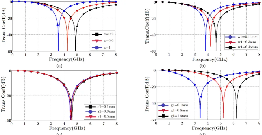
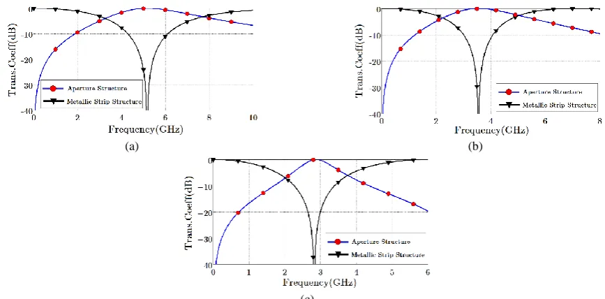
transmission response in terms of increasing “x” are illustrated in Fig. 5(a). By increasing w1, while the
length of the surface currents path is approximately constant, its width is increased. Therefore, the inductance values of both of the screens decrease. On the other hand, this change does not have any effect on the effective length or gap width between two adjacent cells, and so the capacitance value of the cell. Fig. 5(b) depicts the changes in frequency response of the screens caused by increasing w1. As can be observed from
Fig. 5(c), in overall, increasing s1 does not have any
noticeable effect on the effective width and length of surface currents path. In the other words, the effects of increasing or decreasing approximately counteract each other. Nevertheless, this change causes the decrease in the effective length of capacitive gap between the two adjacent cells and as a result, the capacitance value of the cell is enhanced.
The enhancement of the g1 value in this structure
causes the decrease of effective length and thus the cell inductance value. However, the effective width of the surface currents path is approximately constant. In addition, the existing gap between the two adjacent cells
is increased and the cell capacitance value is decreased. According to the electric fields shown in Fig. 4, the air gaps in the cell do not have a vital role in the creation of the structure's capacitance. Fig. 5(d) shows the frequency response of the structure in terms of increasing g1. In this case, it should be noted that
excessive increase of g1, causes the inconvenient grating
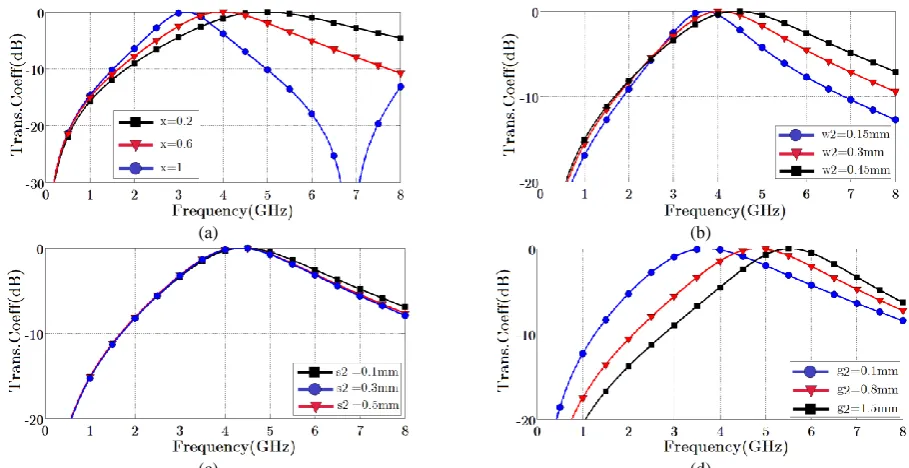
lobes which appears at oblique incidence angles [1]. Similar arguments lead to the frequency responses depicted in Fig. 6. However, as previously mentioned, the brief results are given in Table 2.
According to the assertion of this paper, considering the above-mentioned discussion, a desired filtering characteristic can be achieved by separate engineering of each frequency response. For example, to decrease or increase the center frequency, the same changes of inductance and capacitance values of the screens are required (or at least the changes in one while the other is constant). This requirement is achieved by δ1, δ2, δ3, g1
parameters of the metallic strip structure and δ1, δ2, δ3,
g2 of the aperture structure. The results of these
variations are shown in Figs. 7(a) and 7(b), and the corresponding geometric parameters are given in Tables 3 and 4. On the other hand, the low or high quality factor of final dual-band filter depends on the quality factors of each screen. It is clear that, as the quality factor of band pass filter resulting from the aperture structure becomes higher, the second-order frequency response has a sharper roll off. In other words, an intelligent control on the changing of that group of geometric parameters is needed, which create a change in opposite directions in the inductance and capacitance values or at least approximately do not have any influence on one of them. Therefore, the geometric
(a) (b)
(c) (d)
Fig. 5 Investigating the effect of increasing a) δ1, δ2, δ3, b) w1, c) s1, and d) g1 on the frequency response of the metallic strip
structure with the substrate thickness of t = 0.787 mm.
Iranian Journal of Electrical and Electronic Engineering, Vol. 15, No. 2, June 2019 176
parameters w1, s1 in the metallic strip structure and w2,
s2 in the aperture structure will be useful. A prototype of
the above-mentioned design is done in such a way that the resultant frequency responses have high quality factors. The results are shown in Fig. 7(c) and corresponding geometric parameters of the screens are given in Table 5.
2.3 Filtering Characteristic of Dual Band Structure
Up to here, the filtering specifications of the first-order structures are investigated. Now, the main claims of the paper can be justified based on the optimization of the final second-order filter structure from both of the first-order screens. As previously mentioned, the dual-band structure includes two metallic screens and a substrate with the thickness of t = 1.575 mm.(The reason for selecting this option was discussed previously) as shown in Fig. 8(a). The corresponding equivalent circuit model is illustrated in Fig. 8(b), in which the metallic strip and aperture screens are modeled as a series and parallel LC resonator, respectively. As before, the substrate between the screens is modeled as a
transmission line with characteristic impedance of
0/
c r
Z Z . The substrate permeability (μr), the
distance between two screens, the length and thickness of the metallic strips and their relative positions to each other affect the value of the mutual inductance (M). In the provided scenario, this parameter can be ignored in comparison with L1, L2. At this stage, the second-order
filters with the prenominated geometries of “Geometry 1, 2, 3, 4” are simulated and their results are given in Fig. 9(a). This figure confirms our claim based on the separate controlling of the first-order filtering specifications. The first geometry is the one was proposed in [15]. The second geometry that is composed of high center frequency first-order screens with higher center frequency. The third, which is composed of low center frequency first-order structures also has a center frequency that is smaller than the first geometry. Finally, the last structure, whose geometrical parameters are given in Table 5, has our desired filtering characteristics. Its center frequencies are 1.9 GHz and 3.1 GHz and it has sharp pass bands and so can be recognized as a practical dual-band filter in 2~6 GHz.
(a) (b)
(c) (d)
Fig. 6 Investigating the effect of increasing a) δ3, δ4, δ5, b) w2, c) s2, and d) g2 on the frequency response of the aperture structure
with the substrate thickness of t = 0.787 mm.
Table 2 Reviewing the effects of increasing the geometric parameters of metallic strip and aperture structures on the unit cell inductance and capacitance.
Geometric parameters (Q) (f0) (C) (L) Geometric parameters (Q) (f0) (C) (L)
δ1 ↑ ↓ ≃cte ↑ δ4 ↑ ↓ ≃cte ↑
δ2 ↑ ↓ ≃cte ↑ δ5 ↑ ↓ ≃cte ↑
δ3 ↑ ↑ ≃cte ↑ δ6 ↑ ↓ ≃cte ↑
w1 ↓ ↑ ≃cte ↓ w2 ↓ ↑ ↓ ≃cte
s1 ≃cte ≃cte ≃cte ≃cte s2 ↑ ≃cte ↑ ↓
g1 ↑ ↑ ↓ ↓ g2 ↑ ↑ ↓ ↓
Iranian Journal of Electrical and Electronic Engineering, Vol. 15, No. 2, June 2019 177
(a) (b)
(c)
Fig. 7 Investigating the effects of smart choice of geometric parameters on frequency responses for: a) Decreasing the center frequency (The center frequency of the metallic strip and aperture structures have moved to 5.17 GHz and 5.18 GHz, respectively–
Geometry 2), b) Increasing the center frequency (The center frequency of metallic strip and aperture structures have moved to frequencies of 3.55 GHz and 3.56 GHz, respectively–Geometry 3), and c) Increasing the quality factors of each screen (Geometry 4).
Table 3 The employed geometric parameters of screens in Fig. 7(a) in [mm].
δ1 δ2 δ3 δ4 δ5 δ6 s1 w1 g1 s2 w2 g2
1.8 1.1 0.4 0.2 0.2 0.2 0.4 0.4 0.8 0.4 0.4 0.4
Table 4 The employed geometric parameters of screens in Fig. 7(b) in [mm].
δ1 δ2 δ3 δ4 δ5 δ6 s1 w1 g1 s2 w2 g2
4 2.3 0.6 0.8 0.4 0.4 0.4 0.4 0.8 0.4 0.4 0.1
Table 5 The employed geometric parameters of screens in Fig. 7(c) in [mm].
δ1 δ2 δ3 δ4 δ5 δ6 s1 w1 g1 s2 w2 g2
4.3 2.7 1.1 3.6 2 0.4 0.4 0.4 0.1 0.9 0.1 0.4
(a) (b)
Fig. 8 a) The unit cell schematic of second-order filter and b) corresponding equivalent circuit model.
(a) (b)
Fig. 9 Comparison of the frequency response of second-order filters with: a) different geometries and b) different substrates (Rogers RT5880: εr = 2.2, tanδ = 0.0009, Rogers RO4450B: εr = 3.3, tanδ = 0.004, Rogers TMM4: εr = 4.4, tanδ = 0.002).
Iranian Journal of Electrical and Electronic Engineering, Vol. 15, No. 2, June 2019 178
The corresponding geometric parameters, which are investigated in the previous section, have been obtained by a compromise between quality factor and center frequency. It is emphasized that unlike most studies, the performances of this prototype have been achieved using the screens that are not geometrically complementary. At the end of this part, it is noteworthy that in addition to the listed degrees of freedom, the frequency response of the double-screen structure can also be adjusted by the relative permittivity of the employed substrate (εr). An enhancement in the value of
this parameterwill increase the capacitance values of both of the screens. This results in sharper pass bands with lower center frequencies. Fig. 9(b) shows the frequency responses of the second-order filter with “Geometry 4” for several substrates.
3 Second-Order Filter for WLAN and GSM Frequencies
By keeping the worthiness of all foregoing discussions, the range of changes in geometrical parameters of some unit cells are limited. For example in the presented unit cell the horizontal and vertical metallic strips conflict with each other for high values
of δi = 1,…,6. This limitation persuades us to introduce
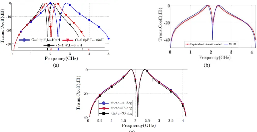
another method by using lumped elements to design a highly selective filter with practical applications (Figs. 10(a) and (b)). The employed lumped elements have standard geometric quantities which are extracted from the manufacturer companies [34, 35] in order to keep the practical aspect of proposed design method. Fig. 11(a) shows the desired frequency response that was designed using the geometric parameters of Table 1 and the lumped elements. A highly selective tunable dual-band band-pass frequency selective filter for center frequencies of 1.8 GHz and 2.4 GHz are achieved by
C = 0.75 pF, L = 15 nH. Simulation results for the proposed structure show a good angular stability performance. To validate the performance of the optimized structure, the result of the equivalent circuit model also is depicted in Fig. 11(b). The results for the incidence angles of θ = 0, 15°, 30° are given in Fig. 11(c). As can be seen in Fig. 11(a), the achieved frequency response has two symmetrical pass bands with acceptable insertion losses. Furthermore, the proposed structure with two closely-spaced pass bands is an appealing candidate for WLAN and GSM filtering applications.
(a) (b) (c)
Fig. 10 The manner of embedding the lumped inductors and capacitors in metallic strip and aperture screens and the resultant ECM are shown in a), b), and c), respectively.
(a) (b)
(c)
Fig. 11 a) Comparison of the frequency response of second-order filters with different values of lumped inductor and capacitor, b) Comparison of the method of moment and equivalent circuit method for the optimized structure, c) Evaluating the stability of
proposed second-order filter against the variation of incident angle for the case 9
Iranian Journal of Electrical and Electronic Engineering, Vol. 15, No. 2, June 2019 179 5 Conclusions
In this paper, an intelligent non-trial-and-error method for the design of double screen frequency selective surfaces is discussed. Using some physical institution and an equivalent circuit model, it is shown that the specifications of the resultant second-order filter can be predicted by separate tuning of each screen. The equivalent circuit results have good agreement with the full-wave simulations. It was then investigated that in some instances, the geometrical parameters of the employed unit cell did not have the capability for full range tuning. To adjust the specifications of our desired second-order frequency response, using lumped elements, a miniaturized band-pass filter with high selectivity for GSM (1.8 GHz) and WLAN (2.4 GHz) applications was designed. Simulation results showed the angular stability of the dual-polarized proposed frequency selective surface.
References
[1] B. A. Munk, Frequency selective surface: Theory and design, John Wiley & Sons, New York, 2000.
[2] M. R. Da Silva, C. D. L. Nóbrega, P. D. F. Silva, and A. G. D'Assunção, “Dual‐polarized band‐stop FSS spatial filters using vicsek fractal geometry,”
Microwave and Optical Technology Letters, Vol. 55, No. 1, pp. 31–34, Jan. 2013.
[3] M. Fallah and M. H. Vadjed-Samiei, “Designing a bandpass frequency selective surface based on an analytical approach using hexagonal patch-strip unit cell,” Electromagnetics, Vol. 14, No. 2, pp. 217– 228, Dec. 2015.
[4] J. Song and P. F. Dixon, “Shielding structures including frequency selective surfaces,” U.S. Patent, No. 9,173,333, Oct. 2015.
[5] M. Fallah, A. Ghayekhloo, and A. Abdolali, “Design of frequency selective band stop shield using analytical method,” Journal of Microwaves, Optoelectronics and Electromagnetic Applications, Vol. 35, No. 1, pp. 25–39, Dec. 2014.
[6] S. Hashemi and A. Abdolali, “Room shielding with frequency-selective surfaces for electromagnetic health application,” International Journal of Microwave and Wireless Technologies, Vol. 9, No. 2, pp. 291–298, Mar. 2017.
[7] J. Roberts, K. L. Ford, and J. M. Rigelsford, “Secure Electromagnetic Buildings Using Slow Phase Switching Frequency Selective Surfaces,”
IEEE Transactions on Antennas and Propagation, Vol. 64, No. 1, pp. 251–261, Jan. 2016.
[8] M. Z. Joozdani, M. Amirhosseini, and A. Abdolali, “Wide band radar cross section reduction of patch array antenna with miniaturized hexagonal loop frequency selective surface,” Electronics Letters, Vol. 52, No. 9, pp. 767–768, Apr. 2016.
[9] M. Bouslama, M. Traii, A. Gharsallah, and T. A. Denidni, “Analysis of antenna gain enhancement using new frequency selective surface superstate,” Microwave and Optical Technology, Vol. 58, No. 2, pp. 448–452, Feb. 2016.
[10]M. Mehrabi, H. Rajabalipanah, A. Abdolali, and M. Tayarani, “Polarization-insensitive, ultra-broadband, and compact metamaterial-inspired optical absorber via wide-angle and highly efficient performances,” Applied Optics, Vol. 57, No. 14, pp. 3693–3703, May 2018.
[11]M. Rahmanzadeh, A. Abdolali, A. Khavasi, and H. Rajabalipanah, “Adopting image theorem for rigorous analysis of a perfect electric conductor– backed array of graphene ribbons,” JOSA B, Vol. 35, No. 8, pp. 1836–1844, Aug. 2018.
[12]A. Momeni, K. Rouhi, H. Rajabalipanah, and A. Abdolali, “An information theory-inspired strategy for design of re-programmable encrypted graphene-based coding metasurfaces at terahertz frequencies,” Scientific Reports, Vol. 8, No. 1, p. 6200, Apr. 2018.
[13]H. Rajabalipanah, H. Hemmati, A. Abdolali, and M. Amirhosseini, “Circular configuration of perforated dielectrics for ultra-broadband,
wide-angle, and polarization-insensitive
monostatic/bistatic RCS reduction,” IET Microwaves, Antennas & Propagation, Vol. 12, No. 11, pp. 1821–1827, Apr. 2018.
[14]A. Abdolali, M. Rajabalipanah, and
H. Rajabalipanah, “Ultra-thin tunable plasma-metasurface composites for extremely broadband electromagnetic shielding applications,” Progress In Electromagnetics Research, Vol. 85, pp. 91–104, 2018.
[15]X. D. Hu, X. L. Zhou, L. S. Wu, L. Zhou, and W. Y. Yin, “A miniaturized dual-band frequency selective surface (FSS) with closed loop and its complementary pattern,” Antennas and Wireless Propagation Letters, Vol. 8, pp. 1374–1377, Dec. 2009.
[16]S. N. Azemi, K. Ghorbani, and W. S. T. Rowe, “Angularly stable frequency selective surface with miniaturized unit cell,” Microwave and Wireless Components Letters, Vol. 25, No. 7, pp. 454–456, Jul. 2015.
Iranian Journal of Electrical and Electronic Engineering, Vol. 15, No. 2, June 2019 180
[17]S. Sheikh, “Miniaturized-element frequency-selective surfaces based on the transparent element to a specific polarization,” IEEE Antennas and Wireless Propagation Letters, Vol. 15, pp. 1661– 1664, Jan. 2016.
[18]M. Nauman, R. Saleem, A. K. Rashid, and M. F. Shafique, “A miniaturized flexible frequency selective surface for X-band applications,” IEEE Antennas and Wireless Propagation Letters, Vol. 58, No. 2, pp. 419–428, Feb. 2016.
[19]M. Rahmanzadeh, H. Rajabalipanah, and A. Abdolali, “Analytical investigation of ultrabroadband plasma–graphene radar absorbing structures,” IEEE Transactions on Plasma Science, Vol. 45, No. 6, pp. 945–954, Jun. 2017.
[20]K. Rouhi, H. Rajabalipanah, and A. Abdolali, “Real‐time and broadband terahertz wave scattering manipulation via polarization‐insensitive conformal graphene‐based coding metasurfaces,” Annalen der Physik, Vol. 530, No. 4, p.1700310, Apr. 2018.
[21]M. Baharian, H. Rajabalipanah, M. H. Fakheri, and A. Abdolali, “Removing the wall effects using electromagnetic complex coating layer for ultra-wideband through wall imaging,” IET Microwaves, Antennas & Propagation, Vol. 11, No. 4, pp. 477– 482, Oct. 2016.
[22]A. Vahidi, H. Rajabalipanah, A. Abdolali, and A. Cheldavi “A honeycomb-like three-dimensional metamaterial absorber via super-wideband and wide-angle performances at millimeter wave and low THz frequencies,” Applied Physics A, Vol. 124, No. 4, pp. 337, Apr. 2018.
[23]M. Rahmanzadeh, H. Rajabalipanah, and
A. Abdolali, “Multilayer graphene-based
metasurfaces: robust design method for extremely broadband, wide-angle, and polarization-insensitive terahertz absorbers,” Applied Optics, Vol. 57, No. 4, pp. 959–968, Feb. 2018.
[24]A. Edalati and K. Sarabandi, “Wideband, wide angle, polarization independent RCS reduction using nonabsorptive miniaturized-element frequency selective surfaces,” IEEE Transactions on Antennas and Propagation, Vol. 62, No. 2, pp. 747–754, Feb. 2014.
[25]K. Chang, S. Il Kwak, and Y. J. Yoon, “Equivalent circuit modeling of active frequency selective surfaces,” in IEEE Radio and Wireless Symposium, Orlando, FL, pp. 663–666, 2008.
[26]F. Costa, A. Monorchio, and G. Manara, “An overview of equivalent circuit modeling techniques of frequency selective surfaces and metasurfaces”,
Applied Computational Electromagnetics Society Journal, Vol. 29, No. 12, pp. 960–976, Dec. 2014.
[27]H. Y. Yang, S. X. Gong, P. F. Zhang, F. T. Zha, and J. Ling, “A novel miniaturized frequency selective surface with excellent center frequency stability,” Microwave and Optical Technology Letters, Vol. 51, No. 10, pp. 2513–2516, Oct. 2009.
[28]J. Y. Xue, S. X. Gong, P. F. Zhang, W. Wang, and F. F. Zhang, “A new miniaturized fractal frequency selective surface with excellent angular stability,”
Progress In Electromagnetics Research Letters, Vol. 13, pp. 131–138, 2010.
[29] G. Bharti, K. R. Jha, G. Singh, and R. Jyoti, “Design of dual-polarized and angular stable new bandpass frequency selective surface in X-band,”
Telecommunication Systems, Vol. 61, No. 3, pp. 559–567, Mar. 2016.
[30]W. Li, T. Zhang, G. Yang, and Q. Wu, “A novel frequency selective surface with improved miniaturization performance”, Journal of Electromagnetic Analysis and Applications, Vol. 4, No. 3, pp. 108–111, Mar. 2012.
[31]S. Baisakhiya, R. Sivasamy, M. Kanagasabai, S. Periaswamy, “Novel compact UWB frequency selective surface for angular and polarization
independent operation,” Progress In
Electromagnetics Research Letters, Vol. 40, pp. 71– 79, 2013.
[32]H. Y. Yang, S. X. Gong, P. F. Zhang, F. T. Zha, and J. Ling, “A novel miniaturized frequency selective surface with excellent center frequency stability,” Microwave and Optical Technology Letters, Vol. 51, No. 10, pp. 2513–2516, Oct. 2009.
[33]Y. Yang, X. H. Wang, H. Zhou, “Dual-band frequency selective surface with miniaturized element in low frequencies,” Progress In Electromagnetics Research Letters, Vol. 33, pp.167-175, 2012.
[34]Garret Electronics Corp, [online]. Available: http://www.garrettelec.com.
[35]Bourns Surface Mount Chip Inductor Capability Matrix, Product Selection Guide, [online]. Available: http://www.bourns.com.
H. Rajabalipanah was born in Tehran, Iran, in 1993. He received the B.Sc. and M.Sc. degrees from the Iran University of Science and Technology (IUST), Tehran, Iran all in Electrical Engineering, in 2014 and 2016, respectively. He is currently pursuing the Ph.D. degree in Electrical Engineering with the Iran University of Science and Technology (IUST), Tehran, Iran. His current research interests include metamaterials/metasurfaces, radar cross section (RCS) and RCSR, metamaterial absorbers, graphene-based wave manipulation schemes, metamaterial-based antennas, and through wall imaging.
Iranian Journal of Electrical and Electronic Engineering, Vol. 15, No. 2, June 2019 181 M. Fallah was born in Iran. He received
the M.Sc. degree from Iran University of Science and Technology (IUST) in 2012. His research interests include wave propagation in anisotropic and inhomogeneous media, scattering, and periodic structures such as frequency selective surfaces and metamaterials.
A. Abdolali was born in Tehran, Iran, in 1974. He received the B.Sc. degree from the University of Tehran, Tehran, the M.Sc. degree from the University of Tarbiat Modares, Tehran, and the Ph.D. degree from the Iran University of Science and Technology (IUST), Tehran, all in Electrical Engineering, in 1998, 2000, and 2010, respectively. He joined the Department of Electrical Engineering at IUST, where he is an Associated Professor of Electromagnetic Engineering. His current research interests include electromagnetic wave scattering, radar cross section, radar absorbing materials, cloaking, metamaterials, and wave propagation in complex media, frequency selective surfaces, and bioelectromagnetic.
© 2019 by the authors. Licensee IUST, Tehran, Iran. This article is an open access article distributed under the terms and conditions of the Creative Commons Attribution-NonCommercial 4.0 International (CC BY-NC 4.0) license (https://creativecommons.org/licenses/by-nc/4.0/).