© Shiraz University
A NEW STRUCTURE FOR CURRENT-MODE CONTINUOUS TIME GM-C FILTERS
*S. J. AZHARI
**AND M. SHOKOUFI
Faculty of Electrical Engineering, Iran University of Science and Technology (IUST), Narmak, Tehran, I.R. of Iran, 1684613114
Email: [email protected]
Abstract– In this paper a new structure for the MLF (Multi Loop Feedback) Gm-C group of filters is presented, granting the advantages of both current-mode and fully balanced topologies to the conventional structure of the group.
The ability of the structure to perform even more transfer functions (Low pass and Band Pass) than other members of the group is proved. Methods of enabling the proposed structure to perform other popular transfer functions are also presented. The favorite feature of systematical generation of the structure facilitates its arrangement for any order.
For practical comparison, a Butterworth 4th–order LP filter with a cut-off frequency of
10MHz is designed in three different structures viz; the proposed one, the single-ended current mode, and fully balanced voltage mode. Simulation results show that the PSRR+,PSRR-,CMRR, Noise, THD, DR, consumed power (P) and Figure of Merit (FOM) of the new structure compared to its voltage mode counterpart are improved at least by factors of 36643, 59841, 4.75, 76, 2, 2.45, 1.17 and 509500, respectively. Compared to single ended current-mode type they are improved by factors of 40, 73, not defined, 1.3, 7.8, 150, 0.68 and 1763000,respectively. Although the above mentioned comparison, due to both the similarity of the used technology and the completeness of the results, is the most equitable one for the most definite conclusion, to further widen the extent of the comparison, the proposed structure is also compared with some other works yet assumed as its closet counterparts. This latter comparison also proves the certain superiorities of the proposed structure such that its FOM is from 8500 to 4512740 times larger than those of others. Closer tracking of the input signal at pass-band and more attenuation at stop-band are also achieved by this structure. These results strongly support the theoretical suggestions. Most favorably the much higher PSRR of the new structure makes it an extremely suitable choice for Mix-Mode (System-On- a Chip, SOC/SOI) applications where power supplies (and analog blocks) suffer severely from digital noise.
Keywords– Current-Mode filters, fully-balanced filters, very high FOM filters, very high PSRR/CMRR, very low THD filters, very low noise filters, very wide dynamic range filters
1. INTRODUCTION
In recent years a great deal of attention has been focused on Gm-C based filters, originating from such advantages as; high frequency operation, convenience of full integration, electronical tuning, calculation of components, and systematic generation of any order, a more flexible and simpler structure, and the smaller size of the topology, which matches well with the VLSI requirements [1-14].
There are many variants of Gm-C filters [1]-[14], among which the Multi loop Feedback (MLF) type has gained a distinguished place due to having all the advantages of the group. Moreover, it is less sensitive, more stable and capable of being configured with minimum components [4], [5], [7], [14]-[16]. It has been arranged in both voltage-mode and current-mode structures [1]-[5], [7], [14]-[16].
Due to the unique capabilities of current-mode structures, particularly in performing mathematical operations of filters' transfer functions [3]-[6],[9],[10], [12], [14],[15],[17]-[31], many current mode filters have been designed for which, compared to voltage mode counterparts, such advantages as wider bandwidth, broader dynamic range, lower THD, better inter modulation performance, and non-linear gain compression, multifunction canonic structure, smaller size, lower consumed power and lower power supply are reported [2]-[6],[9],[10],[12],[14],[15] and [17]-[31]. However, concerning MLF Gm-C filters, voltage mode types have more often been approached [4], [7], [11], [16] and [32].
Since fully balanced topologies offer such advantages as high CMRR and PSRR, low THD and noise and high accuracy [2], [11], [16] and [31]-[36], voltage mode versions of MLF Gm-C filters have frequently been implemented in this topology [11], [16], [32] and [34], while it has not yet been arranged for current mode MLF Gm-C filters to the best of the authors’ knowledge. Hence by doing so, if possible, a very desirable continuous-time filter which exploits the outstanding capabilities of both fully balanced and current mode structures will be available. Meanwhile, to date, few works are claimed as implementations of fully balance current-mode filters [13]-[15] and [20]-[23]. However, these claims raise the two following objections. 1) None of these works have reported the values of such differential parameters as CMRR and PSRR, leaving the readers with just a bare claim that has to be supported by strong sufficient proof to be convincing. As exceptional cases [22] has reported the value of CMRR only, and [13] has given values of CMRR and PSRR, but both works (like all others) are liable to second objections as follows, 2) Some of those works are of voltage-mode type [13], and none are of MLF type but [15], again, has not reported the values of CMRR and PSRR, besides it is very heavy, noisy and power consuming.
In this paper, the structural feasibility of the idea of "current mode MLF Gm-C filter" is first practiced. The general theory and formulation of the proposed structure as well as its systematic development for any transfer function of any order are then given. To practically confirm the theory, simulation results of an LP Butterworth filter implemented in this new structure are included. Since a type-to type, spec- to-spec comparison has rarely been attempted the filter is also designed in two other leading configurations of MLF Gm-C filters viz, fully balanced voltage-mode (FBVM) and single ended current-mode (SCM). Their most important parameters are then compared.
2. FEASIBILITY STUDY OF THE IDEA
a) General structure
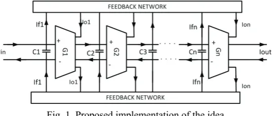
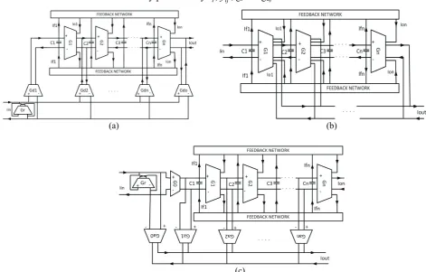
The structure shown in Fig. 1 seems to be a good candidate to implement the proposed idea;
Fig. 1. Proposed implementation of the idea
forward path (Gm-C integrators) are also of current type, providing a fully current-mode processing discipline for the filter.
Figure 1 shows that not only the feedback network of the filter, but also feed forward section and all Gm-Cs are organized in fully balanced architectures supplying another necessity of the idea. To make this possible, as well as to properly perform the current feedback process (sampling output current- mixing input current) gm-amplifiers with at least four output terminals are used [25],[27]and [32]. For implementing band pass transfer functions two more output terminals are required, as is explained in section 3. It is worth noting that multi-output gm-amplifiers (used in this structure) are favored over the multi-input types which are utilized in voltage mode structure since the former types have a simpler circuitry and consume less power [11], [16], [32] and [34].
Figure 1 also shows that the structure balance is increased and the number of its components reduced by using floating capacitors, but at the expense of employing more costly technologies. Otherwise each floating capacitor can be replaced by two separate grounded ones, each of which is doubled in capacitance and connected to a separate node. The case, however, may increase the probability of the structure imbalance.
It can therefore be concluded that structural implementation of a fully balanced current-mode MLF Gm-C filter is generally feasible. To implement a more detailed structure we need to first investigate the theoretical feasibility as well as the formulation validity of the issue.
b) Theory and formulation
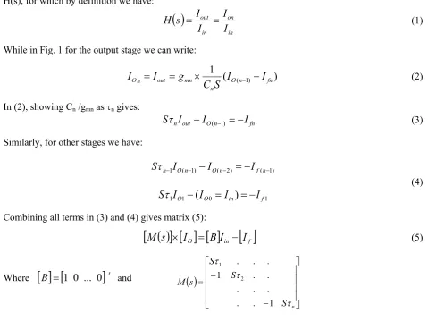
To study the theoretical operation of the proposed structure we develop the relation of its transfer function, H(s), for which by definition we have:
( )
in on
in out
I
I
I
I
s
H
=
=
(1)While in Fig. 1 for the output stage we can write:
1
(
O(n1) fn)
n mn out n
O
I
g
C
S
I
I
I
=
=
×
−−
(2)In (2), showing Cn /gmn as τn gives:
fn n
O out
n
I
I
I
S
τ
−
( −1)=
−
(3)Similarly, for other stages we have:
) 1 ( )
2 ( ) 1 (
1 − − −
− On
−
On=
−
f nn
I
I
I
S
τ
(4)
1 0
1
1
I
O(
I
OI
in)
I
fS
τ
−
=
=
−
Combining all terms in (3) and (4) gives matrix (5):
[
M
( )
s
] [ ] [ ]
×
I
O=
B
I
in−
[ ]
I
f (5)Where
[ ] [
B
=
1
0
...
0
]
t and( )
⎥ ⎥ ⎥ ⎥
⎦ ⎤
⎢ ⎢ ⎢ ⎢
⎣ ⎡
− −
=
n S S
S
s M
τ τ
τ
1 . .
. . .
. . 1
. . .
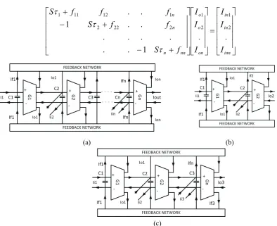
In this structure we arranged a canonic feedback network built by only short circuit connections between arbitrary outputs and inputs so that we have:
[ ]
I
f=
[ ][ ]
F
I
0 ,[ ] [
I
f=
I
f1I
f2...
I
fi...
I
fn]
t,
[ ] [
I
0=
I
01I
02...
I
0i...
I
0n]
t (6) In (6)[ ]
I
0,
[ ]
I
fand
[ ]
F
are matrices presenting output currents of integrators, input currents of feedback networks and feedback factors relating each If to the appropriate Io (i.e. fij is the factor by which Ifi is related to Ioj; Ifi∝
fij.Ioj), respectively. Superscript (t) stands for transpose which is the type of matrices. They are all defined by (3) to (5).Combining (6) into (5) with some manipulation gives;
[
A
(
s
)
] [ ] [ ]
×
I
0=
B
I
in (7)( )
[ ]
[
( )
] [ ]
⎥ ⎥ ⎥ ⎥ ⎦ ⎤ ⎢ ⎢ ⎢ ⎢ ⎣ ⎡ + − + − + = + = nn n n n f S f f S f f f S F s M s Aτ
τ
τ
1 . . . . . . . . 1 . . 2 11 2 1 12 11 1 (8)Thus for H
( )
s we have:( )
[ ]
( )
( )
1 0 1 1 ... ... out n n iin in n i
B
I Io
H s
I I A s A s E s E s E S E
= = = = =
+ + + + +
⎡ ⎤
⎣ ⎦ (9)
Equation (9) is an all pole function proving that the proposed structure behaves like an n-ordered low pass filter, thus it is theoretically feasible too.
3. IMPLEMENTATION OF OTHER FUNCTIONS
Since performing all filter functions requires structures with general (arbitrary finite zero) transfer functions [7], [16] as is shown in (10) rather than all-pole type (9), the proposed structure seems to be of limited application.
( )
0 1 0 1 1...
...
...
...
E
S
E
S
E
S
E
D
S
D
S
D
S
D
s
H
i i n n m n i n n+
+
+
+
+
+
+
+
+
+
=
− (10)Since the same limitation exists in such leading types of MLF Gm-C filters as voltage-mode and single ended current-mode, some methods have been devised to overcome the problem [7],[10], [11], [16].
Although the same methods work properly here as will be discussed later, favorably the proposed structure on its own can perform BP and finite zeros functions as follows.
a) Selectable I/O method
In this method, as is shown in Fig. 2, in an n-ordered filter, ideally “n” pair of terminals exist for input or/and output signals which can arbitrarily be selected depending on the required transfer function.
⎥ ⎥ ⎥ ⎥ ⎦ ⎤ ⎢ ⎢ ⎢ ⎢ ⎣ ⎡ = ⎥ ⎥ ⎥ ⎥ ⎦ ⎤ ⎢ ⎢ ⎢ ⎢ ⎣ ⎡ ⎥ ⎥ ⎥ ⎥ ⎦ ⎤ ⎢ ⎢ ⎢ ⎢ ⎣ ⎡ + − + − + inn in in on o o nn n n n I I I I I I f S f f S f f f S . . 1 . . . . . . . . 1 . . 2 1 2 1 2 22 2 1 12 11 1
τ
τ
τ
(11)(a) (b)
(c)
Fig. 2. Selected I/O implementation of the proposed idea (a): general structure (b): 2nd order filter (c): 3rd order filter
Although finding the general n-ordered transfer function of Fig. 2a is possible by solving (11) it is very tedious and time consuming, thus in this work as an example the equation is solved only for 2nd and 3rd order filters as follows.
1. Second order filter: A Second-order version of the proposed structure with two possible inputs and two possible outputs is shown in Fig. 2b. Solving (11) for n=2 obtains four different transfer functions, the formulation and the types of which are shown in (12) and Table 1.
(
1 11)(
2 22)
122 1 11 1 12 22 2 02 01 . 1 f f S f S I I f S f f S I I in in + + + ⎥ ⎦ ⎤ ⎢ ⎣ ⎡ ⎥ ⎦ ⎤ ⎢ ⎣ ⎡ + − + = ⎥ ⎦ ⎤ ⎢ ⎣ ⎡
τ
τ
τ
τ
(12)Table 1 specifies that if, for example, the input signal is applied to the input port of the 2nd stage (Iin2) and the output signal is taken from the output port of the same stage, the proposed structure can behave like either a BP or LP filter depending on the parameters values of the transfer function of this particular choice, which is defined in (13).
(
1)
(
2 22)
1222 2 11 1 f f S f S f S I I in o + + + + =
τ
τ
τ
(13)Table 1. Types of 2nd order filters realized by selected
2. Third order filter: The structure, formulations and types of the transfer functions of the 3rd-order selectable I/O version of the proposed structure are shown in Fig. 2c, Eq. (14) and Table 2, respectively.
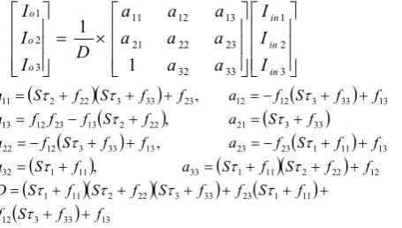
⎥ ⎥ ⎥ ⎦ ⎤ ⎢ ⎢ ⎢ ⎣ ⎡ ⎥ ⎥ ⎥ ⎦ ⎤ ⎢ ⎢ ⎢ ⎣ ⎡ × = ⎥ ⎥ ⎥ ⎦ ⎤ ⎢ ⎢ ⎢ ⎣ ⎡ 3 2 1 33 32 23 22 21 13 12 11 3 2 1 1 1 in in in o o o I I I a a a a a a a a D I I I (14) ( )( ) ( ) ( ) ( ) ( ) ( ) ( ) ( )( ) ( )( )( ) ( )
( 3 33) 13 12 11 1 23 33 3 22 2 11 1 12 22 2 11 1 33 11 1 32 13 11 1 23 23 13 33 3 12 22 33 3 21 22 2 13 23 12 13 13 33 3 12 12 23 33 3 22 2 11 , , , , f f S f f S f f S f S f S D f f S f S a f S a f f S f a f f S f a f S a f S f f f a f f S f a f f S f S a + + + + + + + + = + + + = + = + + − = + + − = + = + − = + + − = + + + = τ τ τ τ τ τ τ τ τ τ τ τ τ τ τ
Table (2) shows that eight different types of BP and nine different types of LP filters can be realized by this structure.
Table 2. Types of 3rd order filters realized by selected I/O method
IO3 IO2 IO1 I/O choice LP BP/LP BP/LP Iin1 BP/LP BP/LP BP/LP Iin2 BP/LP BP/LP BP/LP Iin3
These examples show that selectable I/O method does not need any further components and is preferred to those methods which add supplementary circuits to the basic structure. However, it cannot implement HP and BS functions for which other methods should be examined.
b) Supplementary circuits' methods
Two methods are reported to enhance the all-pole transfer function of fully-balanced voltage-mode and single-ended current-mode MLF Gm-C filters to arbitrary finite zeros type [7], [10] and [16]. They add two different supplementary circuits to the main structure. Although the final structure becomes more complex, massive, noisy and power consumptive than the selectable I/O type, it is capable of producing all filtering functions.
In this section we investigate the possibility of applying the same methods to the new structure as follows.
1. Input signal distributing method: In this method, in general, the input signal is concurrently applied to all nodes of the filter by a distributed network of Gm-amps, hence changing the overall transfer function. Examples of realized structures for fully balanced voltage mode and single ended current mode filters are given in [4], [16] and [10]. To apply the method to the new structure we designed a new distributing network compatible with a fully balance current-mode topology as is shown in Fig. 3a. To derive H(S) we follow the same procedure as obtaining (9), noting that here each node is also driven by distributed network, hence matrix [B] of (5) should be changed to:
[ ]
B
=
[
α
1α
2...
α
j...
α
n]
,
α
j=
g
dj/
g
r (15)While
α
j,
g
r andg
dj are the transmission factor of the input current of jth integrator, gm parameters of input Gm-amp, and of jth Gm-amp, respectively. Fig. 3a also shows:r do on
in
out
I
I
g
g
I
=
α
0.
+
,
α
0=
/
(16)( )
( )
( )
( )
S
A
S
A
S
A
I
I
S
H
n
j j jn
in
out
∑
=+
=
=
0 1α
α
(17)
In (17) Ajn(S) is
j
nthword of matrix [A(S)]. Equation (17) shows that the general structure and itsdeveloped version have the same poles determined by
τ
i andf
ij coefficients, while the latter also includes transmission zeros arbitrarily produced byτ
i,
f
ij, gr and gdj.
(a) (b)
(c)
Fig. 3. Realization of arbitrary finite zero filters by the proposed structure using methods of a) input current distribution b) direct summation c) indirect summation of output currents
2. Output signals summation method: In this approach a supplementary network is connected to the basic structure in such a way to provide an overall output as the sum of different nodes signal. Realization examples of the method for other configurations can be found in [4], [7], [10], and [16]. However two implementations of the method for the proposed structure are given in Figs. 3b and 3c. In Fig. 3b two more output terminals are provided for each Gm-amp except the last one (Gn). A summing network which is arranged by parallel connection of these terminals sums up the output currents of different stages forming the overall output current of the filter. Since both feedback and feed forward networks remain intact, the basic structure maintains the poles and the summing network forms the transmission zeros of the structure. Transmission coefficients can be determined by arbitrarily connecting or disconnecting the respective pair of new terminals. The magnitude of coefficients can be obtained by the aspect ratios (W/L) of the current mirror transistors responsible for new terminals. A negative sign when required is provided by interchanging the related connections. The problem with this realization is inflexible. That is, neither transmission coefficients nor design possible errors can be adjusted after fabrication. However it offers the advantages of simplicity, small size, less consumed power and less noise.
gm-amp (Ga0) of the summation network. As a result gm coefficients of Gm-amps of the summation network can be automatically or manually adjusted to zero or nonzero values for different applications. Summation network can also be wired up (connecting, disconnecting, interchanging) externally according to the required transmission zeros. The problems with this approach compared to the former are: circuit complexity, larger size, more consumed power and more noise. So one may choose either upon the circumstances. To find H(S), considering Fig. 3c we have matrix [B] of (5) as:
[ ] [
....
]
t,
0r
g
B
r o o
r
g
=
=
(18)Also, for Iout we have:
o ao j aj j OJ n J J in out
g
g
B
g
g
B
I
B
I
r
B
I
=
×
×
+
∑
=
=
=1 0
0
,
,
(19)In which gao-gaj and go-gj are mutual transconductance of the Gm-amps of the summation and feed forward network, respectively. Referring to (6) - (8), (18) and (19) IoJ can be obtained by (20) in which
A
1j( )
s
is the 1Jth word of matrix [A(s)]:
( )
( )
inj oj
I
s
A
s
A
r
I
=
1 (20)Now using (19) and (20) we can find H(S) of Fig. 3c as (21) whose type is exactly the same as of (10).
( )
( )
( )
( )
s A s A B s A B r I I s H J J n j o in out 1 1∑
= + × × == (21)
Comparing (21), (17) and (9) shows that also here, the poles are produced by the general section of the proposed structure while the supplementary circuit is responsible for the arbitrary finite transmission zeros.
4. SIMULATION RESULTS AND DISCUSSION
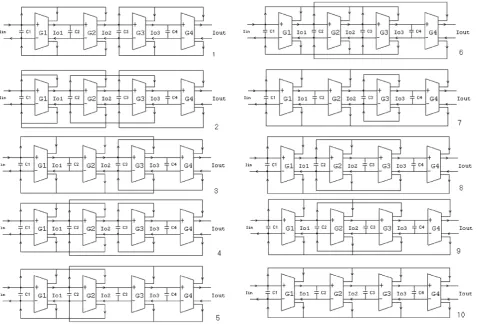
To practically investigate the performance of the new structure, a 4th order Butterworth LP filter is designed. Based on what is explained in [9] and [16] ten different structures shown in Fig. 4 are also possible for canonical MLF fully balanced current mode 4th order LP filter.
All of the Gm-amps of the filter are configured as is shown in Fig. 5 with transistors aspect ratios shown in Table 3. Gm-amplifier is designed so that when biased by ±3V power supplies, providing bias currents of 45µA for differential amplifier (M1-M2) and bias currents of 225µA for output current mirrors (M5-M8, M11-M18), and its gm-value is calculated as 185µS.
Table 3. Aspect ratios of MOSFETs that are used in the Gm-amp
(W/L) Transistor
1/5
2 1,M M 2/2 18 15 13 12 8 6 4
3,M ,M ,M,M ,M ,M ,M
M 5/1 17 16 14 11 7
5,M ,M ,M ,M ,M M
88/2
Fig. 4. Canonical fully balanced current mode structures of 4th order Butterworth low pass filters
Fig. 5. The designed gm-amp
Table 4. Simulation results of the used Gm-amp Simulation results Specification
±3V Supply voltage
175.751MHz Cut- off frequency
1.1 %@3Vp-p,500KHz THD
185µs gm
58.4db PSRR+
34.8db PSRR-
82db CMRR
Till 175.75Mhz 7.62pA Hz
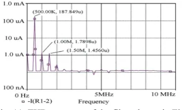
Total at filter pass band 24.1nArms
Noise
6.6mW Power dissipation
Table 5. Capacitors’ values calculated for proposed structures of Fig. 4 while begin used to implement the given 4th order Butterworth filter
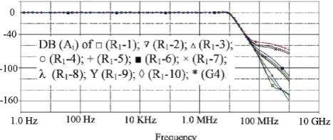
Fig. 6. Comparison of frequency responses of filters which are shown in Fig. 4 (R1-1 to R1-10) with an ideal response (G4)
THD behavior as well as simulated values of the most important specification of this structure operating at
±3V supplies are shown in Fig. 7 and Table 6.
Fig. 7. THD performance of the simulated 4th order fully balanced current mode low pass filter
Figure 7 shows the great advantage of the new structure in rejecting even harmonics and reducing odd ones producing a THD of 0.18% (-55db) while driven by an input current signal with frequency of
C4 C3 C2 C1
500KHz and a p-p amplitude of 400µA (9 times larger than the bias current of dif. Amp., M1-M2). This
shows a nearly 6 fold improvement compared to gm-amp THD, thanks to fully balance scheme which also
significantly improved the PSRR, CMRR and DR of the filter. Using conventional definition for current mode case [38] CMRR, PSRR+, and PSRR- were measured as infinite (here 600db due to the predetermined resolution default of the simulation software) for the ideal transistors of the filter.
Table 6. Simulation results of the given 4th order fully balanced current mode LP filter at
volts Vs=±3 Simulation results
Specification
0.978 AI
0.18%@400µAp-p,500KHz THD
600db Ideal
50.5db MC(WC)*
CMRR
600db Ideal
136.64db MC(WC)*
PSRR+
600db Ideal
136.64db MC(WC)*
PSRR-
4.5 pA/ Hztill 1MHz 36 nArms total noise at
passband Noise
143.77db D.R(THD=0.18%@Iin=400µApp)
10.4MHz Cut off frequency
45.3mW Power dissipation
*Monte Carlo (Worst case) simulation for 10% Vt mismatches
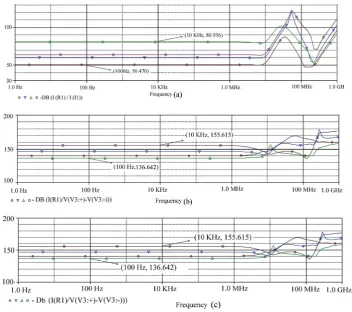
To get a realistic understanding, Monte Carlo analysis allowing 10% mismatches for Vt of the
transistors was executed showing the worst case values as 50.5 db, 136.64db, 136.64db for CMRR, PSRR+, PSRR-, respectively (Table 6 and Fig. 8).
To calculate DR, the definition shown as (22) is adopted [28], taking the values of the parameters from Table 6 and Fig. 12.
The very high value of 143.8db is calculated for DR of the proposed structure at THD of 0.18%, which is basically due to both the low value of THD and the noise of the fully-balance scheme. To compare, the same filtering function is implemented and examined in two other favorite structures of the group as follows.
(
)
(
)
22
% @
noise
THD a
signal
DR= rms (22)
a) Single-ended current mode (SCM) structure
This structure is a well known frequently used one whose 4th-order LP version can be configured in ten different forms [8]. They are realized and their frequency responses for Butterworth LP function with 10MHz cut-off frequency are shown in Fig. 9 [31]. It is worth noting that in this structure gm-amps need
only two output terminals resulting in a smaller size than that of the current work (Figs. 4-5).
Fig. 9. Frequency responses of all possible structures of single-ended current mode version of the filter of instance
Both theory [4], [7], [8] and simulation (Fig. 9) show that the structure of Fig. 10 (labeled as R1-2 in Fig. 9) is the closest- to-ideal one (G4 in Fig. 9) and thus, is chosen for comparison. The values shown in Figs. 11-13 and Table 7 are found for the SCM structure at the same conditions as of Table 6.
Fig. 10. Single-ended current mode structure chosen for comparison
Fig. 11. THD response of the filter shown in Fig. 10
Table 7. Simulation results of the unbalanced current mode version of the given filter at Vs=±3volts
Simulation results Specification
0.942 AI
1.32%@400µAp-p,500KHz
THD
111.6db Ideal
104.5db MC(WC)*
PSRR+
108.7db Ideal
99.4db MC(WC)*
PSRR-
8.9 pA/ Hz till 1MHz
44.24 nA rms total noise at pass band Noise
100.2db DR @ (THD = 0.18%@Iin=400µApp)
10.95MHz Cut off frequency
30.4mW Power dissipation
*Monte Carlo (Worst case) simulation for 10% Vt mismatches
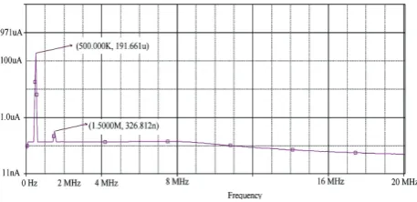
Fig. 12. Noise comparison between new structure ( ), single ended type (◊) and OTA (∇)
b) Fully balanced voltage-mode (FBVM) structure
As is expressed in [7] this structure can also appear in ten different versions, while being used to implement a 4th-order MLF canonical Butterworth LP filter. Among these versions the one in Fig. 14 shows the best performance and so is used for comparison.
To build the special gm-amps (with 4 input and 2 output terminals and Gm=185µS) of the structure two of the Gm-amps used in the SCM version (Fig. 10) are combined with their output terminals connected in parallel.
With filter cut-off frequency of 10 MHz, the following values are calculated for the capacitors [7], [31];
Fig. 13. Monte Carlo analysis of single-ended structure (Fig. 10) in the same condition as of Fig. (8), a) PSRR+, b) PSRR- (ideal pass is not included)
Fig. 14. Fully balanced voltage mode counterpart of the new structure
Frequency response simulation of this structure compared with the ideal response of the type is shown in Fig. 15 and the simulation results of its most important parameters are shown in Table 8 and Figs. 16-18.
Table 8. Simulation results of the fully balanced voltage mode version of the given filter at Vs=±3V Simulation results
Specification
0.9601 Av
0.42%@2.85Vp-p,500KHz
THD
600db Ideal
36.96db MC(WC)*
CMRR
600db Ideal
45.36db MC(WC)*
PSRR+
600db Ideal
41.1db MC(WC)*
PSRR-
74.7 nV/ Hz till 1MHz
272µVrms total noise at pass band
Noise
10.868MHz Cut of frequency
137.7db D.R THD=0.18%@Vin=2.15Vpp)
52.9mW Power dissipation
*Monte Carlo (Worst case) simulation for 10% Vt mismatches
Fig. 16. THD response of the fully-balanced voltage mode filter of Fig. 14
As an important technological advantage, the components count of the new structure is about 2/3 that of the FBVM version which results in; integration easiness, chip size and cost reduction, as well as less power consumption (here 20%), however, this condition is reversed compared to the SCM structure. Better input tracking (gain of the filter) at pass band and more attenuation at stop band (cf. Figs. 6, 9 and15) are other merits of the new structure
The most important parameters in comparing filters efficiency is believed to be; Power Dissipation (P), (characteristic) Frequency (Fo), Tuning Range (
Δ
f), and Dynamic Range (or S/N at a specified level of THD), while CMRR and PSRR are especially important in mixed-mode chips. To encapsulate all these factors a parameter called Figure Of Merit (FOM) is defined [20], [24]. This is very usual in analog continuous time circuits, contrary to digital circuits that work based on discontinuous time signals [25].In this work, since (Fo) is intentionally set fixed and equal for all three structures, we have expressed FOM as:(DR @ 0.18%THD) PSRR CMRR
FOM
P
× ×
= (23)
In (23) the PSRR is the average value of PSRR+ and PSRR- which are very important parameters in mixed-mode where filters are integrated on the same chip with digital circuits.
or those with Monte Carlo simulation results are chosen (with the exception of [15], the only CM. FB. MLF one and [21]). Since the reported results of other works (with the exception of current work) are neither complete nor belong to the same parameters, for a fair comprehensive comparison, four FOMs other than (23) are defined as follows:
FOM1 =CMRR PSRR F0
THD P
× ×
× , FOM2 = 0
CMRR F THD P
×
× (24)
FOM3 = F0 N DR
P
× ×
, FOM4 = F0 N
THD Noise P
×
× ×
Fig. 17. Monte Carlo analysis of fully-balanced voltage mode structure in the same conditions as of Fig. 8, a) CMRR, b) PSRR+, c) PSRR-
They are used to evaluate the overall performance of [13], [21], [15 and20], and [22] while current work structures are evaluated by FOM of (23) and FOM4, since the latter is the only one which includes the value of noise. The table shows that FOM of the new structure is 1763000 times and 509500 times better than those of single-ended Current-Mode and Fully-Balanced Voltage-Mode structures, respectively. It is from 8500 to 451274 0 times larger than other works (3456100 times larger than another MLF one reported by other authors [15]).It also shows that, the new structure has integrated the fully-balanced scheme advantages such as; less THD, larger CMRR, PSRR and DR with the current-mode superiorities resulting in much larger improvement for those advantages which are in common in both fully balanced and current mode schemes.
Table 9. Comparing important parameters of single-ended current mode and fully balanced voltage mode filter and some other close works with those of proposed structure.
Ref. No. [13] [15] [20] [21] [22] CM, Single
ended (This work)
VM, FB (This work)
CM , FB This work (Proposed) Filter type 3rd order VM,FB,
Chebyshev
5th order,
CM,FB, MLF
3rd order, CM,
Dif. Butterworth
3rdorder, CM
Dif. wave Active
13thorder,
CM, dif. wave active
4th order
CM-MLF
4th order
FB-VM-MLF
4th order
FB-CM-MLF
Technology Fabricated in 0.18µm
0.18µm Fabricated 65nm
0.35µm Fabricated 0.35µm
0.5µm
(MC)1 0.5µm (MC)1 0.5µm (MC)1
F0 150K~ 23MHz 28M~44MHz 1M~4MHz 1M~10MHz 4.1MHz 10.95MHz 10.868MHz 10.4MHz
CMRR -37db NA NA -90db~ -50db NA NA 36.96db 50.5db
PSRR -35db NA NA NA NA 104.5db 45.36db 136.64db
THD 0.25% -0.63% @
Vin=100mV
1% @10MHz @Iin=600µA
1%@277µA@ 100KHz
1.78%@Iin= 64µA
0.5%@500K Hz
1.32%@400µA p-p500KHz
0.42%@2.85 Vp-p,500KHz
0.18%@400µ Ap-p,500KHz
DR NA 62-67db 74db~68db
@Vin=0.5V
NA NA 100.2db 137.7db 143.77db
Vsup NA NA 1V ±2.5 ±2.5 ±3 ±3 ±3
Power 18mW 67mW@30M
Hz
9.6mW 14.8mW 178mW 30.4mW 52.9mW 45.3mW
Noise NA
270nV/ 40pA/ NA 125dbm/H
17.8n/
8.9pA/ 74.7nV/ 4.5pA/
--- --- --- --- --- 4.396×10¹¹ (FOM)
1.52×10¹²
(FOM) 7.75×10
17
(FOM) FOM
8.07×10¹⁴
(FOM1)
4.1×10¹²
(FOM3)
3.14×10¹²
(FOM3)
1.2×10¹³
(FOM2)
1.66×10¹⁵
(FOM4)
2.467×10¹⁸
(FOM4)
7.19×10¹⁴
(FOM4)
1.417
×
1019(FOM4)
1) - MC = Monte Carlo Simulation is performed to get the results
5. CONCLUSION
In this work the fully-balanced current mode version of continuous-time MLF Gm-C filters is successfully implemented. The theory of its operation is thoroughly developed and precisely formulated. The block in its simplest form performs an all-pole transfer function. It can also perform BP functions using selectable I/O method. The claim has been proved by examples. Besides, by some minor modification it gained the capability of performing all conventional filtering functions using methods of input signal distributing, and output signal summation.
pass band and more attenuation at stop band. To practically study the performance superiority of the new structure, a 4th-ordered Butterworth LP filter has been implemented by both the new structure and two other leading structures of MLF Gm-C filters; unbalanced current-mode and fully-balanced voltage-mode types. These three types are compared together and also with some other differential Gm-C filers (preferably current-mode MLF types although so far very few have been reported). The results are in good agreement with the theory and strongly support the superiorities of the proposed structure.
REFERENCES
1. Sanchez-Sinencio, E. & Silva-Martinez, J. (2000).CMOS transconductance amps architectures and active filters: A tutorial. Proc. of IEEE Circuits Devices Syst. Feb, Vol. 147, No.1: pp. 3-12.
2. Ananda Mohan, P.V. (2003). Current-mode VLSI analog filters, design and application. Birkhauser Boston, 3. Ahmad Rania, F., Awad Inas, A. & Soliman Ahmad, M. A. (2006). Transformation method from voltage-mode
Op-Amp-RC circuits to current-mode Gm-C circuits. Circuits Systems Signal Processing, Vol. 25, No. 4, pp. 609-26.
4. Su, H. W. & Sun, Y. (2005). Performance analysis and comparison of multiple loop feedback OTA-C filters.
Journal of Circuits, Systems, and Computers, Vol. 14, No. 4, pp. 1–36.
5. Deliyannis, T. L., Sun, Y. & Fidler, J. K. (1999). Continuous-time active filter design. CRC Press.
6. Qadir, A. & Altaf, T. (2010). Current mode canonic OTA-C universal filter with single input and multiple outputs. 2nd International Conference on Electronic Computer Technology (ICECT2010), pp. 32-34.
7. Sun, Y. & Fidler, J. K. (1997). Structure generation and design of MLF OTA-grounded capacitor filters. IEEE Trans. On CAS-1, Vol. 44, No.1, pp. 1-11.
8. Sun Y., Fidler J. K. (1995). Minimum component multiple integrator loop OTA-grounded capacitor all-pole filters Proc. of IEEE Midwest Symp. On CAS, USA. pp. 983-6
9. Sun Y., Fidler J. K. (1995).High-order current-mode continuous-time multiple output OTA-C filters. IEE 15th Sarag. Colloq. Digital and Analogue Filters and Filtering Systems, U.K.P. 8/1-6.
10. Sun Y., Fidler J. K. (1996). Current-mode OTA-C realization of arbitrary filter characteristics. Electronics Letters, Vol. 32, No. 13, pp. 1181-2.
11. Chiang, D. H. & Schumann, R. (1999). Comparison of magnitude and delay sensitivity in IFLF and cascade Gm-C filters. IEEE Int. Symp. on CAS-II, ISCAS’99, pp. 652-5.
12. Shaker, M. O., Mahmoud, S. A. & Soliman, A. M. (2006). A CMOS fifth-order low-pass current-mode filter sing a linear transconductor. P1043-1046 Circuits and Systems, 2006. ISCAS 2006.
13. Gao, Z., Wang, J., Lai, F., Yu, M. & Zhang, Z. Z. (2009). Wideband reconfigurable CMOS Gm-C filter for wireless Applications, Electronics, Circuits, and Systems, ICECS 2009. 16th IEEE International Conference, pp. 179-182
14. Hwang, Y. S., Chen, J. J., Laiand, J. H. & Sheu, P. W. (2006). Fully differential current-mode third-order Butterworth VHF Gm-C filter in 0.18 µm CMOS. IEE Proc. Circuits Devices Syst., Vol. 153, No. 6, pp. 552-558.
15. Zhu, X., Sun, Y. & Moritz, J. (2008). Design of current-mode Gm-C MLF elliptic filters for wireless receivers, Electronics, Circuits and Systems, ICECS 2008. 15th IEEE International Conference, pp. 296-299.
16. Sun, Y. & Fidler, K. (1998). Fully-balanced structures of continuous-time MLF OTA-C filters. IEEE Int. Conf. Circuits and Systems, pp. 157-60.
17. Sun Y., Fidler J. K. (1997). Current-mode multiple feedback filters using dual output OTAs and grounded capacitors. Int. J. of Circuit Theory and Applications, Vol. 25, pp. 69-80,.
19. Laoudias, C., & Psychalinos, C. (2008). Low-voltage CMOS current-mode filters using current mirrors: two alternative approaches. Electrotechnical Conference, 2008. MELECON The 14th IEEE Mediterranean, pp. 435-440.
20. Heimo, U. & Zimmermann, H. (2008). A1VCurrent-mode filter in 65nmCMOS using capacitance multiplication. IEEE 2008System-on-Chip, 2008. SOC 2008. International Symposium,pp. 1-4
21. Souliotis, G. & Haritantis, I. (2005). Current-mode differential wave active filters. IEEE Transactions On Circuits And Systems—I: REGULARPAPERS, VOL. 52, NO. 1, pp. 93-98.
22. Souliotis, G. & Fragoulis, N. (2006). Differential current-mode tunable wave active filters based on single-ended wave port terminators. IEEE Transactions on CAS—I: Regular Papers, VOL. 53, No. 4, pp. 821-828.
23. Souliotis, G. & Psychalinos, C. (2008). Current-mode linear transformation filters using current mirrors. IEEE Transactions on Circuits and Systems—II: Express Briefs, Vol. 55, No. 6, JUNE2008, pp. 541-5.
24. Chamla, D., Andereas, K., Cathelin, A., Belot, D. (2005). A Gm-C low-pass filter for zero-IF mobile
applications with a very wide tuning rang. IEEE J. of SSC. Vol. 40, pp. 1443-50 25. Shahrtash, S. M. & Haghjoo, F. (2009). Instantaneous wavelet transform decomposition filter for on-line
applications. Iranian Journal of Science & Technology, Transaction B: Engineering, Vol. 33, No. B6, pp. 491-510.
26. Toumazou, C., et.al. (1990). Analogue IC design: the current mode approach. London, Peter Peregrinus, 27. Hsu, C. C. & Feng, W. S. (2000). Structural generation of CM filters using multiple-output OTA. Trans. Fund.
Electronic, Communication, Computer Science, Vol. E 83-A, No. 9, pp. 1778-85.
28. Georgantas, T., Bouras, S., Dervenis, D. & Papananos, Y. (1999). A comparison between integrated current and voltage mode filters for baseband applications. Proc. of 6th Int. Conf. of Electronics, Circuits and Systems, pp. 485-8.
29. Zele, R. H., Allstot, D. J. & Fiez, T. S. (1993). Fully balanced CMOS current-mode circuits. IEEE J. of Solid-State Circuits, Vol. 28. No. 5, pp. 569-75.
30. Sun, Y. & Fidler, J. K. (1995). Structure generation of current-mode two integrator loop dual output-OTA grounded capacitor filters. IEEE Trans. On CAS.- II, Vol. 43, pp. 659-63.
31. Shokoufi, M. (2002). Design of a current-mode fully balanced Butterworth low pass Gm-C filter in CMOS technology. M. Sc Thesis, Iran University of Science and Technology (in Farsi).
32. Glinianowicz, J., Jakusz, J., Szczepanski, S. & Sun, Y. (2000). High-frequency two-input CMOS OTA for continuous-time filter applications, IEE Proc. Circuits Devices Syst., Vol. 147, pp. 13-18.
33. Sansen W. N. C. (2006). Analogd Esign Essentials, Springer.
34. Wyszynski, A. & Schumann, R. (1992). Using multiple-I/P transconductors to reduce number of components in OTA-C filter design. Electronic Lett., Vol. 28, pp. 217-20.
35. Vanpeteghem, CP. M. & Duque-Carrillo, J. F. (1990). A general description of common-mode feedback in fully-differential amp. IEEE Int. symp. On CAS, pp. 3209-12.
36. Saniei, N. & Djahanshahi, H. (2007). A high speed SiGe VCO based on self injection locking scheme. Iranian Journal of Science & Technology, Transaction B: Engineering, Vol. 31, No. B6, pp. 651-662.
37. Baker, R. J., Li, H. W. & Boyce, D. E. (1998). CMOS circuits design, layout, and simulation. IEEE Press. 38. Palmisano, G., Palumbo, G. & Pennisi, S. (1999). Performance parameters of COAs. Proc. of IEEE, ICECS, pp.