Research Article ISSN: 2319-507X Rohan Naik, IJPRET, 2013; Volume 1(8):565-571 IJPRET
Available Online At www.ijpret.com
INTERNATIONAL JOURNAL OF PURE AND
APPLIED RESEARCH IN ENGINEERING AND
TECHNOLOGY
A PATH FOR HORIZING YOUR INNOVATIVE WORKCMOS SECOND GENERATION CURRENT CONVEYORS IMPLEMENTATION IN
0.25µM
ROHAN R. NAIK, H. G. VIRANI
Electronics and Telecommunication Department, Goa College of Engineering, Goa India.
Accepted Date:
27/02/2013Publish Date:
01/04/2013
Keywords
CMOS,
Current Conveyor, COA.
Corresponding Author Mr. Rohan R. Naik
Abstract
CMOS Second Generation Current Conveyor is presented as a
Available Online At www.ijpret.com
I. INTRODUCTION
The past few years have seen a great shift in analog circuit design towards representing signals with current instead of voltage. Current mode signal processing is receiving considerable attention for wideband low voltage operation in digital IC processes [1]. A current conveyor is a three terminal device which when arranged with other electronic element in specific circuit configuration can perform many useful analog signal processing functions. In many ways the current conveyor simplifies circuit design in much the same manner as the conventional operational amplifier (op- amp). This stems largely from the fact that the current conveyor offers an alternative way of abstracting complex circuit functions, thus aiding in the creation of new and useful implementations [2].
II. CURRENT CONVEYOR
A. The CCII±
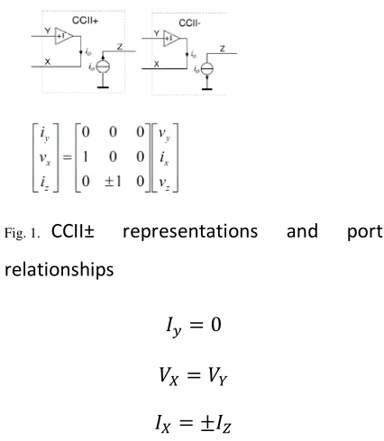
The ideal CCII+ is a three terminal device labeled as X, Y and Z has the following port relations [2][3].
Fig. 1. CCII± representations and port
relationships
= 0
= = ±
The characteristics of CMOS CCII± are stated by means of above equations. An ideal voltage mode circuit possesses infinite input impedance and zero output impedance but the current mode ideal circuits are exactly opposite and are characterized by low input impedance and zero output impendence [3][4].
Research Article ISSN: 2319-507X Rohan Naik, IJPRET, 2013; Volume 1(8):565-571 IJPRET
Available Online At www.ijpret.com
The current conveyor consists of voltage follower input stage Fig. 2 which provides well-conditioned bias currents and output voltages. By setting IB1=IB2=IB and the transistor aspect ratios as follows [4].
= =
Transistors M1, M3 and M2, M4 acquire the same gate source voltages, with the current in M3, M4 being set to n*IB. Assuming transistors with the same bulk-source voltages, M1-M4 provide a translinear loop which reflects the DC voltage of terminal Y on terminal X [4]. The input resistance at terminal X is given by
= +1
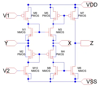
The complete schematic of CCII± implemented with voltage follower given in fig. 3 and fig. 4. Two cascaded complementary current mirror are adopted in the CCII+ while two complementary folded cascade structures is a choice for CCII- [4].
B. Circuit Design for CCII+
Available Online At www.ijpret.com
Fig. 3. Schematic of CCII+
C. Circuit Design for CCII-
Fig. 1 shows the block diagram symbo for a negative second generation current conveyor. The conveyor is characterized by the fact that any voltage that appears at the Y terminal also appears at the X terminal and that any current that flows out of the X terminal also flows out of the Z term Fig. 3 shows the transistor schematic for CMOS current conveyor. Transistors M1 and M3 are designed with the same dimensions, the same dc bias current flowing through them, and the same dc drain source voltage (the same comment applies for M2 and M4, respectively). This means that any change in the voltage at Y will produce a change in current in M1 and thus the same change in current in M3, which in turn produces the
Available Online At www.ijpret.com
Fig. 1 shows the block diagram symbol for a negative second generation current conveyor. The conveyor is characterized by the fact that any voltage that appears at the Y terminal also appears at the X terminal and that any current that flows out of the X terminal also flows out of the Z terminal. Fig. 3 shows the transistor schematic for CMOS current conveyor. Transistors M1 and M3 are designed with the same dimensions, the same dc bias current flowing through them, and the same dc drain source voltage (the same comment applies for M2 and M4, respectively). This means that any change in the voltage at Y will produce a change in current in M1 and thus the same change in current in M3, which in turn produces the
same voltage at X that is at Y. M7 is designed so that the same current that flows in M3 and out of X terminal also flows in M7 and out Z terminal (again, this is true for M3, M7 is also true for M4, M8 respectively)[4][5][6][7].
Fig. 4. Schematic of CCII
The voltage transfer gain A
transfer gain Ai, for the circuits in fig.3 and
fig.4 are given as follows [4].
= =
1
!
"
same voltage at X that is at Y. M7 is designed so that the same current that n M3 and out of X terminal also flows in M7 and out Z terminal (again, this is true for M3, M7 is also true for M4, M8 respectively)[4][5][6][7].
Schematic of CCII-
The voltage transfer gain Av and current
, for the circuits in fig.3 and fig.4 are given as follows [4].
1
1 #$%
#&% #$' #&'
Research Article ISSN: 2319-507X Rohan Naik, IJPRET, 2013; Volume 1(8):565-571 IJPRET
Available Online At www.ijpret.com
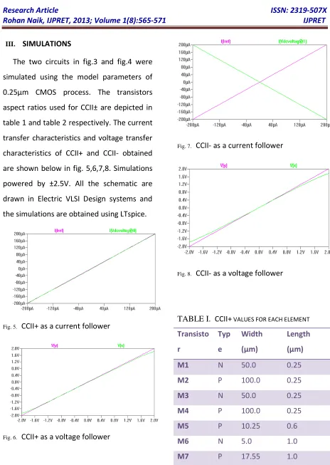
III. SIMULATIONS
The two circuits in fig.3 and fig.4 were simulated using the model parameters of 0.25µm CMOS process. The transistors aspect ratios used for CCII± are depicted in table 1 and table 2 respectively. The current transfer characteristics and voltage transfer characteristics of CCII+ and CCII- obtained are shown below in fig. 5,6,7,8. Simulations powered by ±2.5V. All the schematic are drawn in Electric VLSI Design systems and the simulations are obtained using LTspice.
Fig. 5. CCII+ as a current follower
Fig. 6. CCII+ as a voltage follower
Fig. 7. CCII- as a current follower
Fig. 8. CCII- as a voltage follower
TABLE I. CCII+ VALUES FOR EACH ELEMENT
Transisto
r
Typ
e
Width
(µm)
Length
(µm)
M1 N 50.0 0.25
M2 P 100.0 0.25
M3 N 50.0 0.25
M4 P 100.0 0.25
M5 P 10.25 0.6
M6 N 5.0 1.0
Available Online At www.ijpret.com
M8 N 4.75 1.0
M9 P 16.75 3.0
M10 N 5.5 3.0
V1 1.5V
V2 -1.5V
TABLE II. CCII- VALUES FOR EACH ELEMENT
Transisto
r
Typ
e
Width
(µm)
Length
(µm)
M1 N 50.0 0.25
M2 P 100.0 0.25
M3 N 50.0 0.25
M4 P 100.0 0.25
M7 P 10 1.0
M8 N 2 1.0
IB1 500µA
IB2 500µA
IB3 500µA
IB4 500µA
V1 0V
V2 0V
IV. APPLICATIONS
The CCII± has found applications in active network synthesis, analog computation and input stage for implementation of a current operational amplifier (COA). CCII± bears a strong resemblance to that of op-amp
where the characteristics of system employing CCII± determined by the passive element external to CCII± only [8]. CCII± also have found a broad spectrum of applications such as
• Active filters
• Impendence conversion
• Oscillators
• Instrumentation amplifiers
Acknowledgment
I am deeply indebted to my guide, Mr. H. G. Virani for allowing me to carry out this project under his supervision. He has given me confidence to take up this project and is a pillar of support that I have banked in times of difficulty.
I also wish to thank Prof (Dr.) Rajesh B. Lohani, Head of Department, Electronics and Telecommunication Engineering, for constantly motivating me in my journey through this project.
Research Article ISSN: 2319-507X Rohan Naik, IJPRET, 2013; Volume 1(8):565-571 IJPRET
Available Online At www.ijpret.com References
1. Mucha, I., "Towards a true current operational amplifier [CMOS implementation]," Circuits and Systems, 1994. ISCAS '94., 1994 IEEE International Symposium on , vol.5, no., pp.389,392 vol.5, 30 May-2 Jun 1994
2. C. Toumazou, F.J. Lidgey, D.G. Haigh, Analogue IC Design: the current mode approach, Peter Peregrinus Ltd., Institution of Electrical Engineers, 1990.
3. Fei Yuan, CMOS Current Mode Circuits for Data Communication, Ryerson University, 2007.
4. G. Palmisano, G. Palumbo, S. Pennisi, CMOS Current Amplifiers, Kluwer Acadamic, 1999.
5. Masciotti, J.; Luu, L.; Czarkowski, D., "CMOS current-mode analog circuit building blocks for rf DC-DC converter controllers," Circuits and Systems, 2003. ISCAS '03. Proceedings of the 2003 International Symposium on , vol.3, no., pp.III-455,III-458 vol.3, 25-28 May 2003
6. Parnklang, J.; Nanthanawanitch, W.; Titiroongruang, W., "CMOS current follower
circuits," TENCON 99. Proceedings of the IEEE Region 10 Conference , vol.2, no., pp.1030,1033 vol.2, Dec 1999
7. Luzzi, R.; Pennisi, S.; Scotti, G.; Trifiletti, A., "2-V CMOS current operational amplifier with high CMRR," Circuit Theory and Design, 2005. Proceedings of the 2005 European Conference on , vol.1, no., pp.I/27,I/30 vol. 1, 28 Aug.-2 Sept. 2005