Available Online At www.ijpret.com
INTERNATIONAL JOURNAL OF PURE AND
APPLIED RESEARCH IN ENGINEERING AND
TECHNOLOGY
A PATH FOR HORIZING YOUR INNOVATIVE WORK
IMPROVED PERFORMANCE OF SPLIT CAPACITOR BASED DSTATCOM
FOR SHUNT APPLICATION
RESHAM TONDARE1, S.P. GAWANDE1, A.N.KADU1
Faculty in Department of EEE., YCCE Nagpur.
Accepted Date:
27/02/2013
Publish Date:
01/04/2013
Keywords
VSI,
Hysteresis band current control, Distribution Static Compensator (DSTATCOM),
Instantaneous symmetrical component theory
Corresponding Author Mr. Resham Tondare
Abstract
Available Online At www.ijpret.com
INTRODUCTION
The different power quality problems like
voltage sag , swell , unbalanced , voltage
waveform distortion [2-5]and the
implementation of custom power devices
for the mitigation of various PQ issues are
suggested [5-6]. It was also proposed their
exist different inverter topologies for low
and high voltage distribution system [1]
with the different control strategies
generally used for inverters [6]. The
switching strategy for the inverter
topologies and generating the reference
current from the instantaneous symmetrical
component theory was suggested [6,7]
Power quality is the important issue now a
day’s. Power Quality (PQ) related issues are
of most concern nowadays, the main cause
of power quality problems are power
electronic equipment, information
technology equipments, adjustable speed
drives (ASD),& etc; because of which load
cause disturbance in voltage waveform.
There can be different power quality
problems arises generally in distribution
systems, like voltage sag, swell, unbalanced,
waveform distortion etc. There are certain
power quality issues related to current also,
like unity power factor, voltage regulation
(combinely known as load compensation),
harmonic current compensation, neutral
current compensation etc. Hence the main
aim of load compensation is to get unity
power factor and minimum voltage
regulation.
To mitigate the above mentioned
power quality problems various generalized
methods have been suggested in the
literature. One of the important methods is
by using custom power devices like
Distribution static compensator
(DSTATCOM), Dynamic voltage restorer and
Unified power quality conditioner (UPQC).
Among all the DSTATCOM is a powerful
custom power device having multiple
applications like voltage regulation, unity
power factor and harmonic current
compensation. It is also used to mitigate the
voltage related issues.
In this project different Inverter
topologies are used to implement
DSTATCOM for low and high voltage
distribution system.
DSTATCOM is shunt connected device at
Available Online At www.ijpret.com
current into the line. It basically comprises
of Voltage Source Inverter (VSI) structure
because it can be extended to multilevel,
multi-chain and multi-cells structure. For
low voltage distribution system three
different inverter topologies are used like
three leg VSC with single DC capacitor,
three leg VSC with neutral clamped DC
capacitor and Three phase four leg VSC.
For high voltage distribution system
different inverter topologies are four legs
VSC with single DC capacitor, three leg VSC
with neutral clamped DC capacitors and
three independent single phase inverter
with single dc capacitor.
For modulation different pulse width
modulation (PWM) are used. In this project
all the above topologies will be realized
using hysteresis current controlled pulse
width modulation
and for the generating the reference
current ,the instantaneous symmetrical
component theory will be used.
Different inverter topologies for low voltage
distribution system
a) Three phase three leg inverter with
single dc capacitor.
b) Three phase three leg inverter with
split dc capacitor.
Basic single line diagram of DSTATCOM
Fig(1) DSTATCOM structure.
Above fig (1) shows the single line diagram
of DSTATCOM. It consist of three
components Inverter, interface inductor
and DC link. Hysteresis current control
modulation is used for switching of
DSTATCOM. It is a shunt compensated
device injects the compensated current at
the point of common coupling (PCC).
Reference current generation
Different methods of reference current
generation like Instantaneous PQ theory, PCC
Unbalnced & non linear load
v VL
VSI f
Lf s
is il
+
-Cdc
Vdc
i
Rf
X
Available Online At www.ijpret.com
Synchronous detection technique and
Instantaneous symmetrical component
theory. Instantaneous symmetrical
component theory is the simplest theory to
implement.
The reference currents are generated by
the equations given in (1).
(1)
If we consider inverter losses then the
equations are given in (2).
(2)
Low Voltage distribution system
In a VSC structure, each switch contains an
Insulated Gate Bipolar Transistor (IGBT)
with its associated anti-parallel diode. All
the VSC topologies discussed below for low
voltage distribution systems. It is connected
to three phase four wire(3p4w) system
through interface inductor.
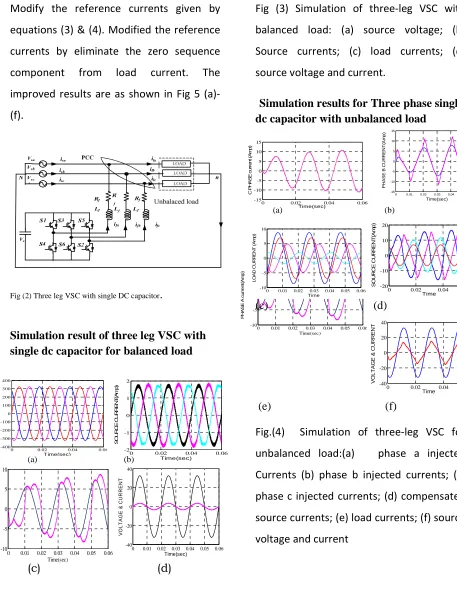
Three leg VSC with single dc capacitor
Fig. 2 shows the schematic diagram of
three leg VSC with single dc capacitor. It
consists of six switches. The operation
depends on the control strategy used.
Hysteresis current control has been used for
the control the switching of the VSC. It
connected to 3p4w system through
interface inductor. The reference current
having zero sequence component but in this
topology not having path to inject zero
sequence component to compensate the
neutral current.
Simulation results are as shown in fig
(3) (a)-(d). For the balanced load with
balanced source there is no need to
compensation. Simulation results for
unbalanced load as shown in fig (4)(a)-(f).
Because of unbalanced load causes zero
sequence current presents in the system at
load side it cause unbalanced to source
voltage as well as source current. But this
Available Online At www.ijpret.com
topology is unable to compensate source
current. Fig. 4(a) and (b) shows tracking of
reference current and injected currents for
only few portion of cycle fails to track phase
‘a’ and ‘b’. Only phase ‘c’ current tracks
exactly as shown in Fig. 4 (c). The loss of
tracking is because the zero sequence
components are present in reference while
VSI is not able to inject the current having
zero sequence components. This topology is
not compensates the source current as well
as not neutralize the neutral current. The
full compensation will not be possible as
the zero sequence components in the load
current. Modify the reference currents
given by equations (7) & (8). Modified the
reference currents by eliminate the zero
sequence component from load current.
The improved results are as shown in Fig 5
(a)-(f).
Three leg VSC with single dc capacitor
Fig. 2 shows the schematic diagram of
three leg VSC with single dc capacitor. It
consists of six switches. The operation
depends on the control strategy used.
Hysteresis current control has been used for
the control the switching of the VSC. It
connected to 3p4w system through
interface inductor. The reference current
having zero sequence component but in this
topology not having path to inject zero
sequence component to compensate the
neutral current.
Simulation results are as shown in fig
(3) (a)-(d). For the balanced load with
balanced source there is no need to
compensation. Simulation results for
unbalanced load as shown in fig (4)(a)-(f).
Because of unbalanced load causes zero
sequence current presents in the system at
load side it cause unbalanced to source
voltage as well as source current. But this
topology is unable to compensate source
current. Fig. 4(a) and (b) shows tracking of
reference current and injected currents for
only few portion of cycle fails to track phase
‘a’ and ‘b’. Only phase ‘c’ current tracks
exactly as shown in Fig. 4 (c).
The loss of tracking is because the zero
sequence components are present in
reference while VSI is not able to inject the
current having zero sequence components.
This topology is not compensates the
Available Online At www.ijpret.com
neutral current. The full compensation will
not be possible as the zero sequence
components in the load current. Modify the
reference currents given by equations (7) &
(8). Modified the reference currents by
eliminate the zero sequence component
from load current. The improved results are
as shown in Fig 5 (a)-(f).
Three leg VSC with single dc capacitor
Fig. 2 shows the schematic diagram of
three leg VSC with single dc capacitor. It
consists of six switches. The operation
depends on the control strategy used.
Hysteresis current control has been used for
the control the switching of the VSC. It
connected to 3p4w system through
interface inductor. The reference current
having zero sequence component but in this
topology not having path to inject zero
sequence component to compensate the
neutral current.
Simulation results are as shown in fig
(3) (a)-(d). For the balanced load with
balanced source there is no need to
compensation. Simulation results for
unbalanced load as shown in fig (4)(a)-(f).
Because of unbalanced load causes zero
sequence current presents in the system at
load side it cause unbalanced to source
voltage as well as source current. But this
topology is unable to compensate source
current.
Fig. 4(a) and (b) shows tracking of
reference current and injected currents for
only few portion of cycle fails to track phase
‘a’ and ‘b’. Only phase ‘c’ current tracks
exactly as shown in Fig. 4 (c). The loss of
tracking is because the zero sequence
components are present in reference while
VSI is not able to inject the current having
zero sequence components.
This topology is not compensates the
source current as well as not neutralize the
neutral current. The full compensation will
not be possible as the zero sequence
components in the load current. Modify the
reference currents given by equations (7) &
(8).
System parameters
Available Online At www.ijpret.com
0 0.02 0.04 0.06
-400 -300 -200 -100 0 100 200 300 400 Time(sec) S O U R C E V O L T A G E (V )
0 0.02 0.04 0.06
-2 -1 0 1 2 Time(sec) S O U R C E C U R R E N T (A m p )
0 0.01 0.02 0.03 0.04 0.05 0.06
-2 -1 0 1 2 Time(sec) L O A D C U R R E N T (A m p )
0 0.01 0.02 0.03 0.04 0.05 0.06
-40 -20 0 20 40 Time(sec) V O L T A G E & C U R R E N T
0 0.01 0.02 0.03 0.04 0.05 0.06 -10 -5 0 5 10 Time(sec) P H A S E A c u rr e n t( A m p )
0 0.01 0.02 0.03 0.04 0.05 0.06 -15 -10 -5 0 5 10 15 Time(sec) P H A S E B C U R R E N T (A m p )
0 0.02 0.04 0.06
-15 -10 -5 0 5 10 15 Time(sec) C P H A S E c u rr e n t (A m p )
0 0.02 0.04 0.06
-20 -10 0 10 20 Time S O U R C E C U R R E N T (A m p )
0 0.01 0.02 0.03 0.04 0.05 0.06
-10 -5 0 5 10 Time(sec) P H A S E A c u rr e n t( A m p )
0 0.01 0.02 0.03 0.04 0.05 0.06
-10 -5 0 5 10 Time L O A D C U R R E N T ( A m p )
0 0.02 0.04 0.06
-40 -20 0 20 40 Time V O L T A G E & C U R R E N T
Modify the reference currents given by
equations (3) & (4). Modified the reference
currents by eliminate the zero sequence
component from load current. The
improved results are as shown in Fig 5
(a)-(f).
Fig (2) Three leg VSC with single DC capacitor.
Simulation result of three leg VSC with single dc capacitor for balanced load
(a) (b)
(c) (d)
Fig (3) Simulation of three-leg VSC with
balanced load: (a) source voltage; (b)
Source currents; (c) load currents; (d)
source voltage and current.
Simulation results for Three phase single dc capacitor with unbalanced load
(a) (b)
(c) (d)
(e) (f)
Fig.(4) Simulation of three-leg VSC for
unbalanced load:(a) phase a injected
Currents (b) phase b injected currents; (c)
phase c injected currents; (d) compensated
source currents; (e) load currents; (f) source
Available Online At www.ijpret.com
0 0.05 0.1
-5 0 5 Time(sec) C U R R E N T (A m p )
0 0.02 0.04 0.06 0.08 0.1
-5 0 5
Time (se c)
C U R R E N T (A m p )B
0 0.01 0.02 0.03 0.04 0.05 0.06
-8 -6 -4 -2 0 2 4 6 8 Time(sec) S o u rc e cu rr en r( A )
0 0.05 0.1
-10 -5 0 5 10 Time(sec) L O A D C U R R E N T (A m p )
0 0.02 0.04 0.06 0.08 0.1
-40 -20 0 20 40 Time(sec) C U R R E N T & V O L T A G E N Vsa Vsb V sc
Vc/2
n
Vc/2
Lf
Lf
Rf
P C C ila
ilb
S 3
ifa ifc L O A D
isc ilc
S5
L O A D
L O A D
Rf isb isa S 4 S 1 S 2 S 6 Lf Rf ifb
U nb alan ced lo ad
3 lc lb la lo I I I
i = + +
(3)
For the modified reference current the
equation is follows
3 ' lo fKr fkr i I
I = −
(4)
Simulation results for unbalanced load with modified reference
(a) (b)
(c) (d)
(e) (f)
Fig.(5) Simulation of three-leg VSC for
unbalanced load with modified reference
currents: (a) phase a injected currents;
(b) phase b injected currents; (c) phase c
injected currents; (d) compensated source
currents; (e) load currents; (f) source
voltage and current.
Improved simulation results are as shown in
Fig (5) (a)-(c) with modified reference
currents but still not compensate the
neutral current.
Three leg VSC with neutral clamped dc capacitor
Fig (6) shows the three leg VSC with neutral
clamped dc capacitor diagram. Zero
sequence current component compensate
by injecting the compensated current into
the line.
Fig(6) Three phase three leg with split dc
capacitor.
0 0.05 0.1
Available Online At www.ijpret.com
In this topology, neutral point of inverter
(N’) connected to neutral of source (N) and
neutral of load (n), which is the path to
inject zero sequence current to neutralized
the zero sequence component at source
side.
The zero sequence components present in
only when the unbalanced or non linear
loads are connected to the 3p4w system.
This topology is able to compensate the
zero sequence current components.
Simulation results of neutral clamped dc
capacitor without dc current as shown in Fig
(7) (a)-(d). Simulation results of neutral
clamped dc capacitor without dc current as
shown in Fig (8) (a)-(d). Connect the dc load
to phase C to increase the dc component it
result shown in Fig(8) (c). In this topology,
there is problem of capacitor balancing to
balanced the capacitor different methods
are suggested.
simulation results of three phase three leg
inverter with split capacitor with
unbalanced load: (a) source voltage;
(b) source current; (c) load current; (d)
Voltage & current of phase a.
CONCLUSION
Three phase three leg with single dc
capacitor inverter not able to compensate
neutral current as
well as not compensate source current.
Three phase three leg with neutral clamped
dc capacitor compensate neutral current
but having capacitor voltage balancing
Available Online At www.ijpret.com
Table 1. System Parameters
REFERENCES
1. A. Ghosh and G. Ledwich, “Power
Quality Enhancement using Custom Power
Devices”, Kluwer, Norwell, May, 2002.
2. Shivkumar Iyer, Arindam Ghosh and
Avinash Joshi, “Inverter topologies for
DSTATCOM applications a simulation
study”, Electrical power systems research
Vol.3, pp. 161-170, Aug. 2005.
3. M. K. Mishra and K. Karthikeyan, “An Investigate on Design and Switching
Dynamics of a Voltage Source Inverter to
Compensate Unbalanced and Nonlinear
Loads’’, IEEE trans. on ind. Elect.,
Vol.56,No.8,Aug. 2009.
4. A. Ghosh and A. Joshi, “A new approach
to load balancing and power factor
correction in power distribution system”,
IEEE Trans. Power Deliv. Vol.15 pp. 417–
422, Jul. 2000.
5. M. K. Mishra, A. Ghosh and A. joshi,
“Control strategies for capacitor voltages
equalization in neutral clamped shunt
compensator”, IEEE Trans. Power Deliv. Vol.
pp.126-130, 2001.
6. M. Azizur Rahman, Tawfik S. Radwan, Ali
M. Osheiba And Azza E. Lashine.“analysis
of current controllers for Voltage-source
Inverter,” IEEE trans. On Ind. Elect.
Vol.44,pp. 477-484,Aug. 1997.
7. M.K. Mishra, A. Ghosh and A. Joshi, “ A
new STATCOM topology to
compensate loads containing ac and dc
components”, IEEE Power Engineering
System parameters
Values of parameters
Source voltages
Balanced sinusoids with Vsa=230∠0
Balanced linear load
Rl + jXl = 120 + j125.6Ω
Unbalanced linear load
Rla + jXla = 30 + j22Ω
Rlb + jXlb = 60 + j31.4Ω
Rlc + jXlc = 120 + j125.6Ω
Non linear
load
R + jX = 150 + j12.56Ω
DSTATCOM When battery used
Vdc = 2 kV, Rf = 0.01Ω,Lf =
40 mH, Rf represents
Available Online At www.ijpret.com
Society Winter Meeting, Singapore, Jan.
2000.
8. R. Vargas, P. Cortes, U. Ammann, J.
Rodriguez, and J. Pont, “Predictive control
of a three-phase neutral point clamped
inverter,” IEEE Trans. Ind. Electron., vol. 54,
no. 5, pp. 2697-2705, Oct. 2007.
9. Anshuman Shukla, Arindam Ghosh,”
Control Schemes for DC Capacitor Voltages
Equalization in Diode-Clamped Multilevel
Inverter-Based DSTATCOM IEEE Trans.On
power delivery, vol. 23, no. 2, April 2008.
10.M. Fracchia, T. Ghiara, M. Marchesoni,
and M. Mazzucchelli, “Optimized
modulation technique for the generalized
N-level inverter, “in proc.IEEE Power
Electron, Spec.Conf. Toledo, Spain, 1992,