Volume 8, Number 4, pp. 359–371.http://www.scpe.org ©2007 SWPS
RAPID AREA-TIME ESTIMATION TECHNIQUE FOR PORTING C-BASED
APPLICATIONS ONTO FPGA PLATFORMS∗
MY CHUONG LIEU†, SIEW KEI LAM†, THAMBIPILLAI SRIKANTHAN†
Abstract. High-level area-time estimation is an essential step to facilitate rapid design exploration for FPGA implementations. Existing works in high-level area-time estimation usually ignore the physical effects of the design after place and route, which have a notable impact on the maximum achievable speed of the design. In this paper, we propose a framework to rapidly estimate the area-time measures of mapping C-applications onto FPGA. The framework relies on the Trimaran compiler to generate an optimized high-level IR (Intermediate Representation) of the C-applications. Area-time estimation of the IR is then performed using a proposed estimation model that is based on an architecture template with application-specific heterogeneous functional units. In order to accurately predict the delay of the design after place and route, we introduce a new metric for the estimation that models the criticality of the design’s interconnectivity. Experimental results based on a set of embedded functions show that the proposed area estimation can achieve comparable results with the synthesis results of a commercial FPGA tool in the order of milliseconds. For the C functions used in our experiments, the proposed delay estimation leads to an average error of about 3% when compared to the post place and route results. In addition, we demonstrate the robustness of the proposed framework which provides consistent results for different FPGA families. The contribution of this paper is a scalable methodology for rapid estimation of cost-benefit metrics of C-based algorithms to be accelerated on FPGA-based high-performance computing platform.
Key words. FPGA, C-based application, area time estimation, hardware accelerator
1. Introduction. FPGAs (Field-Programmable Gate Arrays) have become an attractive solution to meet
the technological and market challenges in embedded processing. Traditional hybrid platforms that incorporate ASIC and microprocessors are migrating towards FPGA platforms (e.g. Xilinx Virtex-II Pro [1] and Altera Stratix [2]) to take advantage of the reconfigurable benefits of FPGA. This trend is supported by the availability of efficient EDA (Electronic Design Automation) tools and the increasingly stringent TTM (Time-To-market) requirements. In order to exploit the strengths in both the microprocessor and FPGA, efficient hardware-software partitioning strategies must be incorporated in the emerging design flows. However, commercially available design flows do not enable designers to make design explorations for effective hardware-software par-titioning. This is chiefly due to a lack of an essential step that can estimate the performance-cost for mapping a software component to hardware early in the design cycle.
In this paper, we propose a framework that can rapidly and accurately estimate the hardware area-time measures for implementing C-applications onto the FPGA. We have chosen C as the input to our framework as it is widely used for embedded processing. The front-end of the framework relies on the high-level optimization and scheduling capabilities of the Trimaran compiler infrastructure [3]. In order to facilitate effective area-time estimations, we have adopted an architecture template for implementing the applications, which is similar to the one proposed in [4]. The architecture template resembles a VLIW-like architecture that incorporates application-specific heterogeneous functional units and register-files, with dedicated interconnection buses.
High-level estimation is performed using an area-time estimation model, which relies on a set of pre-characterized parameters of the components in the architecture template. Previously reported works in high-level area-time estimation often do not consider the interconnect delay of the design after place and route. We will demonstrate that this oversight will lead to high uncertainties in the estimation results. Our proposed approach overcomes this limitation by incorporating a new metric that models the placement complexity of the design’s interconnectivity.
The paper is organized as follows. In the following section, we describe related works in the area of high-level estimation for FPGA implementation. This is followed by an overview of the proposed framework. Section 4 describes the parametric characterization of the architecture template components, and the proposed area-time estimation models. Next, results analysis is provided to demonstrate the benefits of our framework, and we conclude in Section 6.
2. Related Works. Due to the need to expedite the development of complex applications in hardware, a
number of commercial tools that synthesizes high-level languages to FPGA have emerged in recent years. These tools differ in several aspects such as high-level language support, high-level optimization features and the target
∗This research is supported by Infineon Collaboration Fund
†Center for High Performance Embedded System, Nayang Technological University, Singapore {lieu0003, assklam, astsrikan}@ntu.edu.sg}
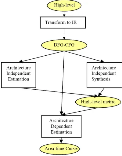
interest in the research community for nearly 20 years. Research efforts in this area are motivated by the need to evaluate the hardware performance-cost indices of various design options early in the design phase, in order to reduce the time-consuming implementation cycles. Figure 2.1 highlights the major steps in a typical high-level estimation flow, which are 1) Transformation of application written in high-level language to IR; 2) Architecture independent estimation; 3) Architecture independent synthesis; 4) Architecture dependent estimation. It is worth noting that previously reported works typically do not address all these steps in their area-time estimation approach. The first step in the estimation flow typically involves the transformation of a high-level representation of an application (e.g. C, System-C, Matlab, behavioral HDL or JAVA specifications) to an IR (Intermediate Representation). This transformation includes high-level compiler optimizations such as loop transformations to extract the hidden parallelism in the sequential C statements. For example, the SUIF [12] compilers have been widely used to transform C-based application into CFGs (Control Flow Graphs) and DFGs (Data Flow Graphs).
Fig. 2.1.High-Level Estimation FLow
Architecture independent estimation attempts to calculate the hardware resources and latency in terms
hardware resources by summing the area of the required operators based on the execution probabilities in the application.
Architecture independent synthesis typically performs scheduling of the IR and resource binding to obtain
accurate high-level metrics, which include the number of clock cycles and hardware resources. The hardware area-time of the application is then calculated or estimated from these metrics. The architecture independent synthesis approach in [16] considers the effects of various loop transformation techniques. Bilavarn et al [17] presented a method that employs architecture independent synthesis for design exploration. However, maximum clock frequency estimation was based solely on the longest latency of the execution unit and ignores post place and route physical effects. Cardoso proposed a methodology for estimating FPGA implementations of Java byte-codes in [18]. He highlighted the limitations of high-level delay estimation due to the lack of circuit details.
Architecture dependent estimation techniques commonly employ simple hardware models to speed-up the
estimation process. The hardware cost is estimated in terms of LUTs (Look-Up Tables), while the performance is often estimated in terms of clock latencies. The technique presented in [19] adopts an analytical approach to estimate the FPGA area for implementing the DFG. The estimation is based on a set of formulas that models the components and corresponding hardware area of the DFG operations. Their approach reported credible results with a maximum error of 10% and the estimation can be achieved in the order of milliseconds. However, they have not considered delay estimation. In [15] , the number of required flip-flops is estimated by calculating the maximum number of required registers. The Rent Rule and Feuer’s formula have been employed to estimate the post place and route interconnect delay. This approach leads to large uncertainty of up to 9 ns. This high uncertainty can become unacceptable for designs that need to be clocked at high frequency (e.g. 100 MHz). It is noteworthy that our proposed area-time estimation accounts for the physical implementation characteristics and is not susceptible to the speed of the design.
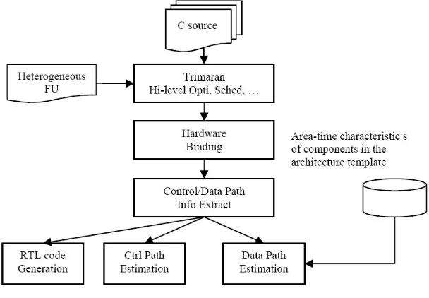
3. Overview of Framework. Figure 3.1 describes an overview of the proposed framework for
high-level area-time estimation. The open-source Trimaran compiler infrastructure, which supports state of the art compiler research in ILP (Instruction Level Parallelism) based architectures, is relied upon to expose the hidden parallelism in the sequential C statements, and to perform high-level optimizations and scheduling [3]. This front-end process takes several seconds (typically less than 10s for 1 single C-function compilation) depending on applications and functions sizes. We have adopted the application-specific architecture template that is similar to the one proposed in [4] as shown in figure 3.2. It is worth mentioning that this architecture template can be adapted for pipelined and non-pipelined data-paths by configuring the application-specific interconnection. The Trimaran machine description is augmented with the heterogeneous functional units in the architecture template. These functional units include a combination of two or more basic operators (e.g. adder, shifter, multiplier, logic operator, comparator and memory-access unit). Only the functional units that are required for a particular application will be incorporated into the architecture.
The output of the Trimaran is an ILP schedule of the application (e.g. the type of functional units that will be executed in each clock cycle and the data-dependency between these functional units). Based on this schedule information, we perform a simple hardware binding process that attempts to bind operations with the most common input-outputs to the same functional units. This aims to reduce the complexity of the interconnectivity between registers and functional units. In order to perform area-time estimation, information pertaining to the control-path and data-path are segregated from the ILP schedule after hardware binding. In this paper, we focus on area-time estimation for the data-path only.
A one-time area-time characterization of the components in the architecture template is required to facilitate area-time estimation of the data-path. An estimation model is then employed along with this information to estimate the performance-cost measures of the application by taking into account the physical implementation effects. In order to evaluate the accuracy of our estimation approach, a process to auto-generate the RTL (Register Transfer Level) codes from the control-data path information has been incorporated in the framework. The RTL code can then be subjected to the FPGA implementation tool (i. e. Xilinx ISE) to obtain the actual post place and route report for results comparison with the proposed estimation approach.
4. Area-Time Estimation. In this section, we will provide detailed description of the process to
charac-terize the components and the proposed area-time estimation model.
4.1. Hardware Characterization of Architecture Template’s Components. We have used the
Fig. 3.1.Propose High-level Estimation Framework
Fig. 3.2.VLIW-like architechture Template
corresponding area-time measures for the Virtex-II Pro device (xc2vp70-6ff1704). The data-paths are assumed to be 16-bit or 32-bit, as the hardware implementation serves to accelerate the base ISA (Instruction Set Architecture) operations of the microprocessor.
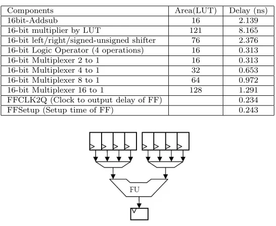
In order to perform interconnect characterization, we have implemented a number of circuits to obtain the average post place and route interconnect delay. The circuits are constructed based on the data-path that is shown in figure 4.1, which resembles the architecture template consisting of a single functional unit. A range of designs, each consisting of up to 8 duplicate circuits similar to the one in figure 4.1, is subjected to physical implementation using the Xilinx ISE tool. We utilized the Xplore Script provided by Xilinx [20] that iteratively executes the place-and-route process to achieve the maximum clock speed. Figure 4.2 shows the maximum delay for the range of designs from which we calculated the average delay after place and route. The average interconnect delay is then computed using Equation 4.1, where Logic Delay is the sum of Clk2q, Mux4to1, functional unit delay, and FF-Set-up time that are listed in Table 4.1. The average interconnect-delay for the target device is found to be 0.42 ns, and this value will be used by the proposed method for delay estimation.
InterconnectDelay= (Avg(M axDelay)−LogicDelay)/3 (4.1)
It is noteworthy that the proposed high-level estimation approach can also be adopted for different target FPGA families by performing a one-time hardware characterization for the particular device.
4.2. Area Estimation. In order to perform area estimation, we obtained the number of functional units
Table 4.1
Characterized Components for Xilinx FPGA Virtex2p-6
Components Area(LUT) Delay (ns)
16bit-Addsub 16 2.139
16-bit multiplier by LUT 121 8.165 16-bit left/right/signed-unsigned shifter 76 2.376 16-bit Logic Operator (4 operations) 16 0.313 16-bit Multiplexer 2 to 1 16 0.313 16-bit Multiplexer 4 to 1 32 0.653 16-bit Multiplexer 8 to 1 64 0.972 16-bit Multiplexer 16 to 1 128 1.291 FFCLK2Q (Clock to output delay of FF) 0.234 FFSetup (Setup time of FF) 0.243
Fig. 4.1.Sample Circuit for Characterizing Average Interconnect Delay
LUTs is computed by summing up the number of LUTs for the functional units based on the pre-characterized information. As each slice of Xilinx Virtex2 pro contains 2 Look-up tables (LUT) and 2 flip-flops, we estimate the total slices as in 4.2:
Estimated number of slices= (#LU T+ #F F)/2 (4.2) The estimation for the number of slices assumes that each slice is fully utilized to implement the functional units and registers. Experimental results reveal that the proposed estimation method is very accurate for LUT and Flip-Flop estimation. In addition, the estimation of the slices is comparable with ISE logic synthesis results and results reported in previous work [15].
4.3. Delay Estimation. The difficulty in delay estimation lies in the prediction of the interconnect delay
before the physical design steps (i. e. placement and routing). There have been several reported works in the area of interconnect delay estimation such as [21] [22] and we will briefly discuss them before describing the proposed delay estimation approach. It is worth mentioning that these previous works are not integrated as part of a high-level estimation framework, but are used mainly to aid optimization decisions in the CAD flow. The work presented in [21] can achieve very accurate estimations of the interconnect delay by analyzing the physical characteristics of the designs. However, due to the complexity of the approach, the estimation results are achieved in the order of seconds and minutes. Karnik and Kang [23] presented an empirical routing delay model for estimating interconnection delays in FPGA. These methods require low-level metrics of circuit such as net fan-out and routing congestion which is not desirable for efficient high-level estimation [18]. Their method resulted in an estimated delay with 20% errors. Hutton highlighted that that delay estimation based on theoretical models, generally produces inferior results when compared to those computed based on empirical data [24]. Manohararajah et. al. reported an interesting finding that the predictability of FPGA implementation is mainly governed by the placement rather than routing process [25].
Fig. 4.2.Maximum post place and route delays for eight designs comprising of multiple of sample circuits (see figure 4.1)
of input/output connections of that register. Compared to the first two characteristics, the fan-in/out provides a better indication on the interconnect complexity of the design. However, during place and route, the CAD tools often perform register duplication to mitigate the fan in/out effect. Our experiments show that although register-duplication can lead to improved timing in some cases, it could also increase the routing congestion of the circuit. This was inferred in our experiments for some designs, whereby the final delay after register duplication is higher than the delay obtained from implementations that obviates register duplication. Due to this uncertainty, we have assumed that the applications employed in our experiments have moderate register reusability and hence, we do not incorporate the fan-in/out characteristic in our delay estimation model.
In this section, we introduce a delay estimation model that takes into account the post place and route characteristics of the design. Our proposed delay estimation model incorporates a new metric that is based on the relative path delays of the design. In contrast to the method in [21], our proposed method can estimate at a higher abstraction level and achieve reasonable results in less than a second. In addition, we will demonstrate that the maximum estimation error of the proposed model is less than 8% for the experiments considered.
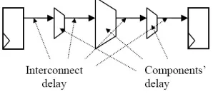
4.3.1. Proposed Approach. A path is a connection of a sequence of logic units that begins and ends at
a register, as shown in figure 4.3. Let’s define Dpath(i) as the delay of a path i in a RTL design,Dmaxas the critical path of that design, andDmean as the mean delay of the paths in the design. Calculations forDpath,
Dmax, andDmean are defined below, which constitutes to a simple delay estimation model. If place and route
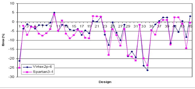
effects are ignored, the minimum clock period is approximate asDmax. We compared the estimated delay of 45 random algorithms using the simple delay model with actual results after place and route for the Xilinx Spartan and Virtex-II Pro device. The estimation error shown in figure 4.4 exhibits a consistent error pattern for the two devices. This serves as the motivation for us to use the simple delay model as a basis for post place and route estimation as it can be employed across different devices. The consistency of the delay predictability on the two different devices implies that the inherent characteristics of the design can be used for estimation. The delay of path i (Dpath(i)) for all the paths in the circuit is computed as follows:
Fig. 4.3.A typical delay path from register to register
Dpath(i) =F FClk2q+Dint+Dcomp+F Fsetup
Dmax= Max of all Dpath
Dmean= Mean of all Dpath
Dcomp is the characterized delay of the component in Table 4.1 (Usually: Mux→ Functional Unit → Mux)
Fig. 4.4. Estimation error of critical paths for 2 FPGA families
As mentioned earlier, our proposed delay estimation model incorporates a new metric that is based on the relative path delays of the design. It has been previously reported that the placement process plays a more important role on the predictability of the final delay (assuming that there is no constraints on the number of FPGA routing resources)[25]. In addition, timing-driven placement relies on the criticality of the nets, and hence the effect of the nets criticality can lead to reliable predictability of the interconnection delay. Based on this, we introduce the lambda metric to compute the relative lengths of nets which capture the complexity of the placement effort for a particular design:
λ= Dmean
Dmax
(4.3)
λcaptures the slack distribution of the nets in the designs. If a circuit has one net that is much longer than the rest (i. e. low-λ), the CAD tool will require lesser effort to place the shorter paths such that they do not exceed the delay of the longest path. On the other hand for a circuit with high-λ, the CAD tool will have less freedom to move the paths around without violating the delay of the longest path. Hence, we expect designs with low-λdesign to be more predictable than designs with high-λ. Our strategy is to identify through empirical means, the threshold value that will categorize a design as low-λor high-λdesigns. Let’s define this threshold value as Λ. The estimated delay of a design with low-λis computed as the maximum path length, while a design with high-λis computed by multiplying the mean path length with a constant factor. The constant factor was empirically found to be close to 1/Λ. The following describes our proposed delay estimation model, whereDest is the estimated delay.
Dest=
Dmax ifλ≤Λ
Dmean×Λ1 otherwise (4.4)
4.3.2. Determining Value of Λ. We compared the estimated delay using the simple delay model with
the actual place and route results for 45 random algorithms. Figure 4.5 shows the estimation error and the correspondingλof the designs. It can be observed that there exist a high correlation between the predictability and λ. In particular, it is shown that for low λ , the simple delay model can be applied with about 90% confidence. Large errors or low predictability are found in region whereλis high. We empirically define Λ to be 0.78 from the dataset.
5. Result Analysis. Table 5.1 describes the properties of the C functions that have been used to
eval-uate the proposed framework for high level area-time estimation. These applications (apart from the random algorithm) are commonly used in embedded applications.
Fig. 4.5.Estimation Error (Predictability) versusλ
Table 5.1
Connectivity Characteristics of Sample Circuits
Funtions DM ean λ Max Avg Max Ave
(ns) Fanout Fanout Fanin Fanin Random Algorithm1 8.66 0.76 6 1.66 2 0.89 Matrix multiplier2 4.25 0.44 2 1.06 1 0.59 mpeg2- bdist1 motion 4.82 0.46 13 2.13 4 1.22 mpeg2- bdist2 motion 4.84 0.47 13 2.07 4 1.20 mpeg2- dct type estimation 4.87 0.51 5 1.43 2 0.81 mpeg2- dist1 motion 5.73 0.88 11 2.43 5 1.08 mpeg2- dist2 motion 5.38 0.50 19 3.25 9 1.92 mpeg2- idctcol 5.63 0.53 15 1.70 2 0.91 mpeg2- idctrow 5.88 0.55 15 1.70 2 0.86 sha transform 4.94 0.84 14 2.60 7 1.65 adpcm coder 4.84 0.73 10 2.54 8 1.35 adpcm decoder 4.64 0.67 9 2.16 9 1.22
5.1. Area Estimation. Table 5.2 compares the proposed area estimation (Pro) with results obtained
from the Xilinx ISE tool after synthesis (Syn) and after place and route (PAR). The last four columns show the estimation errors of our method and that of logic synthesis, when compared with the post place and route values. It is evident that the proposed area estimation achieves up to an average of 98% accuracy, with a worst case error of 8% in terms of LUT comparison. For the estimation of slices, the average error of the proposed method is 12%. It is noteworthy that area estimation in terms of FPGA slices is a difficult task and the majority of the previous works reported their estimation results in terms of LUTs and flip-flops [27] [18] [19]. In general, our proposed area estimation for both LUTs and slices is comparable to the results of the logic synthesis tool. In addition, the proposed estimation can be completed in order of milliseconds, while the compilation time of the commercial synthesis tool takes several minutes (because of the level of abstraction).
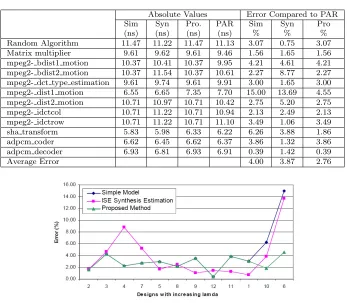
5.2. Delay Estimation. The maximum delay of the above mentioned C-functions were estimated using
the simple delay model (Sim) and the proposed model (Pro), and compared with actual post place and route values. In addition, we have used the ISE Xilinx tool to synthesize and implement the generated RTL codes in order to obtain the estimated delay after synthesis (Syn) and the actual delay after place and route (PAR). The results show that the proposed approach (Pro) outperforms the simple delay model and the synthesis tool for estimating the post place and route delay. In particular, the proposed delay estimation achieves better results in terms of both maximum and average accuracy. The maximum and average estimation error of the proposed approach is only 4.6% and 2.8% respectively. It can be observed from figure 5.1 that the simple delay model can provide accurate estimation results for designs with lowλ cases. However, in designs with high-λ(i. e. 6 and 10), the simple delay model and the synthesis tool (Syn) incurs very high estimation error (i. e. up to 14%). In these cases, the proposed estimation approach is capable of providing significantly better accuracy due to the inclusion of the new metricλthat can be easily obtained for high-level estimation.
5.3. Estimation Runtime. The experiments were carried out on the Pentium 4 3GHz workstation, and
mpeg2- dist1 motion 6.55 6.65 7.35 7.70 15.00 13.69 4.55 mpeg2- dist2 motion 10.71 10.97 10.71 10.42 2.75 5.20 2.75 mpeg2- idctcol 10.71 11.22 10.71 10.94 2.13 2.49 2.13 mpeg2- idctrow 10.71 11.22 10.71 11.10 3.49 1.06 3.49 sha transform 5.83 5.98 6.33 6.22 6.26 3.88 1.86 adpcm coder 6.62 6.45 6.62 6.37 3.86 1.32 3.86 adpcm decoder 6.93 6.81 6.93 6.91 0.39 1.42 0.39
Average Error 4.00 3.87 2.76
Fig. 5.1.Estimation error with designs arranged in increasing ofλ
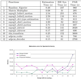
estimation process completes in the order of milliseconds except in cases 3, 4, 6, 7. In these cases, parsing of the Trimaran’s textual output takes up to 2 seconds to complete, while the actual hardware binding and estimation process is performed in milliseconds. Overall, our technique achieves the estimation results about 350 times faster than the synthesis process, and about 3000 times faster than the PAR process.
5.4. Evaluation of the Framework for different FPGA Families. In order to evaluate the robustness
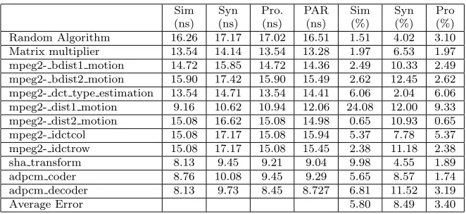
of the proposed framework, we carried out experiments with the Spartan-3 FPGA. The following processes are repeated with the new target FPGA device: 1) characterization of components and interconnect, 2) identification of the value ofλand 3) area-time estimation. Due to the less sophisticated FPGA routing fabric in Spartan-3, we have obtainedλ= 0.72. Table 5.5 and 5.6 show the quality of estimation compared to actual place and route values. The average errors of delay were found to be 3.4% while synthesis tool’s estimation error is 8.5%. The results of the proposed area estimation are reasonably good compared to the results obtain from the synthesis tool. In figure 5.2, the designs are rearranged in increasing order ofλ. It can be observed that there is a large estimation error obtained using the simple model and ISE synthesis tool for designs with high value of λ. In contrast, the estimation error incurred with the proposed technique is consistent across the different functions. This implies that the proposed estimation technique leads to a higher degree of predictability when compared to the simple model and synthesis tool.
6. Conclusions. FPGA-based high-level area-time estimation that ignores the physical design effects after
Table 5.4
Estimation Runtime Compared to Synthesis And Actual PAR time
Functions Estimation ISE Syn PAR Time (s) Time (s) Time (s) 1 Random Algorier 0.26 237 960 2 Matrix Multiplier 0.08 31 285 3 mpeg2- bdist1 motion 2.54 255 676 4 mpeg2- bdist2 motion 2.59 110 814 5 mpeg2- dct type estimation 0.2 35 613 6 mpeg2- dist1 motion 2.89 82 3612 7 mpeg2- dist2 motion 2.71 112 687 8 mpeg2- idctcol 0.23 141 2620 9 mpeg2- idctrow 0.17 107 690 10 sha transform 0.25 152 3600
11 adpcm coder 0.2 81 780
12 adpcm decoder 0.15 61 2700
Fig. 5.2.Estimation error with designs arranged in increasing ofλ
compared to post place and route results obtained from a commercial tool, our proposed delay estimation achieves an average accuracy of 97% with a worst case error of only 4.5%. This result is significantly better than previously reported works in high-level delay estimation and the estimation process can be completed in the order of milliseconds. In addition, we have shown that the proposed framework provide consistent results for devices from the Xilinx Virtex and Spartan families.
REFERENCES
[1] Xilinx Corporation,VirtexII Pro Capabilities. Available athttp://www.xilinx.com/products/silicon solutions/fpgas/ virtex/virtex ii pro fpgas/capabilities/index.htm
[2] Altera Corporation,Stratix II FPGA.Available athttp://www.altera.com/products/devices/stratix2/st2-index.jsp
[3] L. N. Chakrapani, J. Gyllenhaal, W. meiW. Hwu, S. A. Mahlke, K. V. Palem, and R. M. Rabbah, Trimaran: An
infrastructure for research in instruction-level parallelism. In: Lecture Notes in Computer Science (Langurages and
Compilers for High Performance Computing), 2004, pp. 32–41.
[4] R. Schreiber, S. Aditya, S. Mahlke, V. Kathail, B. R. Rau, D. Cronquist, and M. Sivaraman,PICO-NPA: High-level
synthesis of nonprogrammable hardware accelerators. Journal of VLSI Signal Processing, 31(2002), pp. 127–142.
[5] Mitrionics Corporation,Mitron-C.Available athttp://www.mitrionics.com/
[6] Celoxica Corporation,Handel-C.Available athttp://www.celoxica.com/
[7] DSPLogic Corporation,DSPLogic ToolBox.Available athttp://www.dsplogic.com/home/
[8] ImpulseC Corporation,Impulse C language.Available athttp://www.impulsec.com/
[9] Altera Corporation, C to Hardware Technology. Available athttp://www.altera.com/products/ip/processors/nios2/ tools/c2h/ni2-c2h.html
[10] Justin L. Tripp, Maya B. Gokhale, Kristopher D. Peterson,Trident: From High-Level Language to Hardware Circuitry.
Computer, 40(2007), pp. 28–37.
[11] Shawn McCloud, Catapult C Synthesis-based Design Flow: Speeding Implementation and increasing Flexibility.Mentor Graphic White Paper 2003. Available athttp://www.mentor.com
[12] Byongro So et al, Using Estimates from Behavioral Synthesis Tools in Compiler Directed Design Space Exploration.
Proceedings of Design Automation Conference 2003, 2 (2003), pp. 514–519.
Table 5.6
Delay estimation for Spartan3-4 Family
Sim Syn Pro. PAR Sim Syn Pro (ns) (ns) (ns) (ns) (%) (%) (%) Random Algorithm 16.26 17.17 17.02 16.51 1.51 4.02 3.10 Matrix multiplier 13.54 14.14 13.54 13.28 1.97 6.53 1.97 mpeg2- bdist1 motion 14.72 15.85 14.72 14.36 2.49 10.33 2.49 mpeg2- bdist2 motion 15.90 17.42 15.90 15.49 2.62 12.45 2.62 mpeg2- dct type estimation 13.54 14.71 13.54 14.41 6.06 2.04 6.06 mpeg2- dist1 motion 9.16 10.62 10.94 12.06 24.08 12.00 9.33 mpeg2- dist2 motion 15.08 16.62 15.08 14.98 0.65 10.93 0.65 mpeg2- idctcol 15.08 17.17 15.08 15.94 5.37 7.78 5.37 mpeg2- idctrow 15.08 17.17 15.08 15.45 2.38 11.18 2.38 sha transform 8.13 9.45 9.21 9.04 9.98 4.55 1.89 adpcm coder 8.76 10.08 9.45 9.29 5.65 8.57 1.74 adpcm decoder 8.13 9.73 8.45 8.727 6.81 11.52 3.19
Average Error 5.80 8.49 3.40
[14] Chauduri S. and Walker, Computing the lower bound of functional unit before scheduling.IEEE Transactions on Very Large Scale Integration (VLSI) Systems, Vol 4 Issue 2(1996), pp. 273–279.
[15] A. Nayak, M. Haldar, A. Choudhary, and P. Banerjee,Accurate Area and Delay Estimators for FPGA.Proceedings of International Conference DATE, 2002, pp. 862–869.
[16] Minjoong Rim and Rajiv Jain,Estimating performance characteristic of Loop transformation.IEEE International Sympo-sium on Circuits and Systems, 1 (1994), pp. 249–252.
[17] Sebastien Bilavarn et al,Design Space Pruning through estimations of Area/Delay Trade-off for FPGA.IEEE Transac-tions on Computer-Aided Design of Integrated Circuits and Systems, 25(2006), pp. 1950–1968.
[18] Jo˘ao M. P. Cardoso,On Estimations for Compilation of Software for FPGA,Proceedings of the16th International Con-ference on Application-Specific Systems, Architecture and Processors (ASAP’05), 2005, pp. 225–230.
[19] Dhananjay Kulkarni et al,Compile Time Area estimation for LUT-based FPGAs.ACM Transactions on Design Automa-tion of Electronic Systems (TODAES), 11 (2006), pp. 104–122.
[20] Xilinx Corporation, Xplorer Technology. Available at http://www.xilinx.com/products/design tools/logic design/ implementation/xplorer.htm
[21] Min Xu. Fadi J. Kurdahi, Area and timing estimation for lookup table based FPGA.Proceedings of the 1996 European conference on Design and Test, 1996, pp. 151.
[22] Shankar Balachandran,A-priori wirelength and interconnect estimation based on circuit characteristics,Proceedings of the 2003 international workshop on System-level interconnect prediction SLIP, 2003, pp. 77–84.
[23] Tanay Karnik and Sung-Mo Kang,An Empirical Model For Accurate Estimation of Routing Delay in FPGAs.Proceedings of the 1995 IEEE/ACM international conference on Computer-aided design, 1995, pp. 328–331.
[24] Micheal Hutton,Interconnect Prediction for Programmable Logic Devices,Proceedings of the 2003 international workshop on System-level interconnect prediction, 2003, pp. 31–38.
[25] Valavan Manohararajah et al, Difficulty of Predicting Interconnect Delay in a timing driven FPGA CAD Flow, In: Proceedings of International Proceedings on SLIP, 2006, pp. 3–8.
[26] Seong Y. Ohm et al,A comprehensive estimation technique for High-level Synthesis,Proceedings of the 8th international symposium on System synthesis, 1995, pp. 122–127.
[27] Carlo Brandolese et al,An area estimation methodology for FPGA based Designs at system C- level.Proceedings of the 41st annual conference on Design automation, 2004, pp. 129–132.
Edited by: Javier D´ıaz
Received: October 8th, 2007