DOCTORAL THESIS
Linear, nonlinear and
quantum optics in Silicon Photonics
Author:
Supervisor:
Massimo Borghi
Lorenzo Pavesi
Contents
0 The SIQURO project and thesis outline 7
1 Introduction 11
1.1 Silicon photonics building blocks . . . 21
1.1.1 Waveguides . . . 21
1.1.2 Couplers . . . 23
1.1.3 Splitters and combiners . . . 24
1.1.4 Microresonators . . . 25
1.1.4.1 Add Drop and All Pass congurations . . . 26
1.1.4.2 Sequence of coupled resonators: CROW and SCISSOR . . . 29
1.1.4.3 Tuning of microresonators . . . 31
1.1.4.4 Applications of Silicon microresonators . . . 32
1.1.5 Modulators . . . 33
1.1.6 Lasers and photodetectors . . . 34
1.2 Nonlinear Silicon Photonics . . . 35
1.3 Quantum Silicon Photonics . . . 37
2 Chaotic dynamics in coupled resonator sequences 39 2.1 Theory of optical resonators under thermal and free carrier nonlinearities . . . 40
2.1.1 Equation of motion for the eld . . . 41
2.1.2 Rate equations for the carriers and temperature . . . 42
2.1.3 Qualitative discussion of the solutions of the eld equation . . . 43
2.2 Hysteresis, optical limiting and self pulsing of a single cavity . . . 45
2.3 Periodic self pulsing and chaos in coupled resonator sequences . . . 53
2.3.1 System geometry . . . 53
2.3.2 Dynamic time response of the SCISSOR . . . 54
2.3.3 Comparison between periodic and chaotic waveforms . . . 56
2.3.4 Inuence of the input initial conditions on the onset of chaos . . . 59
2.3.5 Theoretical model of the coupled cavity system and computation of the Lyapunov exponents . . . 61
2.3.6 Tuning the onset of chaos with the device geometry . . . 64
2.4 Generation of random bit sequences using chaotic waveforms . . . 66
3 Multimodal Four Wave Mixing in Silicon waveguides 69
3.1 Stimulated and Spontaneous FWM in straight Silicon waveguides . . . 69
3.2 Multimodal phase matching technique . . . 76
3.3 Selective mode excitation in multimode waveguides . . . 78
3.3.1 Interference of two oblique beams . . . 80
3.3.2 Experimental realization . . . 84
3.3.3 Tilted ber approach . . . 88
3.4 Experimental MMFW in straight Silicon waveguides . . . 89
3.5 Future perspectives: use of MMFWM for MIR to NIR conversion . . . 99
3.6 Future perspectives: on chip implementation of two beams interference . . . 101
3.7 Conclusions . . . 102
4 Investigation of strain inducedχ(2) nonlinearities in Silicon waveguides through the elec-tro optic eect 104 4.1 Electro optic eect in titled racetrack resonators: principles and design . . . 106
4.1.1 Principles of the method . . . 106
4.1.2 Design of racetrack resonators . . . 108
4.1.3 AC Electro optic measurements using a Lock In amplier: theory . . . 113
4.2 Device fabrication and passive characterization . . . 116
4.3 AC electro optic measurements using a Lock In amplier: experiment . . . 119
4.3.1 Normal behaviour . . . 120
4.3.2 Not normal behaviour . . . 123
4.3.3 Interpretation of the anomalous behaviour . . . 125
4.3.4 Phenomenological interpretation in terms of trap released free carriers . . . 129
4.3.5 High frequency electro optic measurements . . . 133
4.3.6 Summary and conclusions . . . 137
5 Manipulation of SPDC photon pairs in a Mach Zehnder interferometer 139 5.1 Spontaneous Parametric Down Conversion . . . 139
5.1.1 A brief theory of SPDC . . . 141
5.2 Generation of photon pairs in a periodically poled Lithium Niobate crystal . . . 145
5.2.1 Source characterization . . . 146
5.2.2 Coincidence measurements . . . 149
5.2.3 Spectral properties of the generated radation . . . 151
5.3 One and two photon interference in a free space Mach Zenhder Interferometer . . . 154
5.3.1 Theory of the MZI excited by SPDC photons . . . 154
5.3.1.1 SPDC Light in a MZ Interferometer with Lossless Beamsplitters . . . 160
5.3.1.2 SPDC Light in a MZ Interferometer with Lossy Beamsplitters . . . 160
5.3.1.3 Examples of SPDC Coincidence Patterns for Lossless and Lossy Beamsplitters 161 5.3.2 Experimental results . . . 164
5.3.3 Comparison with other input radiation states . . . 167
5.3.3.1 Classical light . . . 168
5.3.3.2 Independent Photons . . . 168
5.3.3.3 Thermal Light . . . 170
6 On chip integrated networks for the manipulation of quantum states of light 175
6.1 Quantum sources based on racetrack resonators . . . 175
6.2 Quantum sources based on degenerate FWM in multimode waveguides . . . 181
6.3 Pump lter . . . 183
6.4 Phase shifters and delay line . . . 186
6.5 Arrayed Waveguide Gratings . . . 191
6.6 Examples of integrated quantum circuits . . . 194
6.6.1 Recongurable network for the creation and manipulation of N00N and antibunching states . . . 195
6.6.2 On chip Hong Ou Mandel interference with degenerate photon pairs . . . 197
6.7 Summary and conclusions . . . 199
Conclusions 201
List of publications 203
Appendix A: Nonlinear coupled wave theory for optical resonators 204
Appendix B: Linear and nonlinear refractive index changes in straight nanophotonic
waveg-uides 210
Acknowledgements 213
Abbreviations
sFWM Spontaneous Four Wave Mixing SFWM Stimulated Four Wave Mixing FWM Four Wave Mixing
MMFWM Multi Modal Four Wave Mixing MMPM Multi Modal Phase Matching TOE Thermo Optic Eect
TPA Two Photon Absorption SPM Self Phase Modulation XPM Cross Phase Modulation MZI Mach Zehnder Interferometer BS BeamSplitter
AWG Arrayed Waveguide Grating
AP All Pass
AD Add Drop
SCISSOR Side Coupled Integrated Spaced Sequences Of Resonators CROW Coupled Resonator Optical Waveguide
WDM Wavelength Division Multiplexing NIR Near Infra-Red
MIR Mid-Infrared PBG Photonic Band Gap
SPDC Spontaneous Parametric Down Conversion IC Integrated Circuit
OEIC Opto-Electronic-Integrated-Circuit DUV Deep Ultra Violet
LE Lyapunov Exponent
LLE Largest Lyapunov Exponent
CMOS Complementary Metal Oxide Semiconductor SOI Silicon On Insulator
FWHM Full Width at Half Maximum FSR Free Spectral Range
FE Field Enhancement
EDFA Erbium Doped Fiber Amplier VOA Variable Optical Attenuator VNA Vector Network Analyzer
FPR Free Propagation Region
CRIT Coupled Resonator Induced Transparency PPLN Periodically Poled Lithium Niobate
Chapter 0
The SIQURO project and thesis outline
This thesis work has been largely carried out within the framework of the project SIQURO, which started in 2013funded by the Provincia Autonoma di Trento (PAT) [1]. SIQURO covers both fundamental aspects
SPDC Strained silicon
(Chapter 4) Off chip
Interferometers (Chapter 6)
SPDC PPLN (Chapter 5) On chip
Interferometers (Chapter 6) Two photon interference
(Chapter 5)
Chaos in SCISSOR (Chapter 2)
sMMFWM Waveguides (Chapter 3)
sFWM Resonators (Chapter 6)
𝑅𝑒(𝜒(3))
𝐼𝑚(𝜒(3))
|Ψ
𝑜𝑢𝑡
= 𝑈(𝜙)
|Ψ
𝑖𝑛
Figure 1: Illustration of the milestones of the project SIQURO and the thesis chapters in which these are covered. The research on quantum sources is represented by the input state|Ψini, their manipulation by the operator U(φ)and the detection of the output state by|Ψouti.
Except for chapter 2, the research activities of all the other chapters have been carried out within the framework of the SIQURO project. By the way, chapter 2 covers a dierent aspect of the same nonlinearity which will be the subject of chapter 3. The rst is indeed focused on TPA, which is mediated by the imaginary part of the complexχ(3) tensor, while the second deals with FWM, which is instead related to the real part.
By virtue of this fact, and by following the logical streamlines of the project SIQURO, this thesis work will be organized as follows:
Chapter 1 gives an introduction to Silicon Photonics, which is the platform over which the SIQURO project aims to realize the integrated quantum circuits. In the rst part of this chapter, some historical remarks and a general overview of the subject are presented. Then, the chapter focuses on the basic building blocks of a photonic integrated circuit, like waveguides, splitters, resonators, modulators, lasers and photodetectors. This section is intended to oer a brief insight on the physics of the devices that will be implemented in the experiments described in the following chapters, as well to review the state of the art of these components.
all passive, CMOS compatible random number generator.
Chapter 3 is devoted to the study of Multi Modal Four Wave Mixing (MMFWM) in straight Silicon waveguides. The nal goal of this study is the engineering of multimode waveguides for the ecient generation of entangled photon pairs through sFWM. These will constitute a possible on chip integrated source of nonclassical states of light, through which multiphoton manipulation and quantum interference is made possible. Despite the fact that this phase matching technique directly comes from earlier studies in optical bers [2], only few and very simple examples have been reported on a chip [3]. To my knowldge, examples of wavelength conversion in which the pump, the signal and the idler wave propagates in dierent mode orders have never been reported in literature. In chapter 3, MMFWM will be experimentally demonstrated for several modal combinations and waveguide widths. Dierent setups for selective mode excitation will be discussed.
Chapter 4 focuses on the investigation ofχ(2) nonlinearities in strained Silicon waveguides. Within the
framework of the project SIQURO, the nal aim of this work is to exploit the induced second order nonlinearities to generate entangled photon pairs through SPDC. The process would convert a pump photon at1.55µminto two twin photons at MIR wavelengths. These will constitute a possible source
of nonclassical states of light integrated on a Silicon chip, through which multiphoton manipulation and quantum interference is made possible. To probe the existence ofχ(2) eects, the linear electro optic
eect (or Pockels eect) is investigated in strained racetrack resonators using an homodyne detection based on Lock In ampliers. In comparison with previosly reported works, which rely on the static Pockels eect in strained Mach Zehnder interferometers, this technique oer enhanced sensitivity and immunity to noise sources. During this activity, it has been found that free carrier accumulation and depletion at the waveguide boundaries in response to an applied voltage, was the main source of electro optic modulation, which masked anyχ(2)contribution. These observations have been validated by high
frequency measurements, which allowed to disentangleχ(2) eects from free carrier ones on the basis
of the dierent timescales at which the modulation is performed.
Chapter 5 reports on a quantum optic experiment performed by using Infra-Red entangled photon pairs produced by SPDC in a Periodically Poled Lithium Niobate (PPLN) crystal. Such experiment has been preparatory for the future implementations of integrated interferometric structures on a Silicon chip, which is outlined as one of the main goals of the SIQURO project. In the rst part of the chapter, the SPDC source has been characterized. In the second part, the theory of entangled photon propagation in an amplitude unbalanced free space Mach Zehnder interfefometer is presented and experimentally validated. Novel two photon interference eects, which arise from the asymmetric excitation of the device, have been observed. The experiment was preparatory in the sense that the whole theoretical framework can be straightforwardly applied to integrated circuits, provided that the refractive index of the medium in which light propagates is replaced by the eective modal index.
Chapter 6 concerns the future perspectives of the SIQURO project. In particular, the designs of the main elements which compose a complete integrated quantum network are presented and validated through simulations. Such elements include quantum sources based on sFWM in waveguides and resonators, phase shifters and delay lines, pump suppression lters and arrayed waveguide gratings. The main goal of this chapter is to propose an optical nework which includes all the functionalies required to perform a complete quantum optics experiment on a Silicon chip. Only the pump laser and the photodetectors are not integrated and have to be supplied from the outside.
In appendix A, the theory of optical resonators under the simultaneous action of thermal, free carrier andχ(3) nonlinearities is presented. The coupled wave equations for the resonator modes involved in
Chapter 1
Introduction
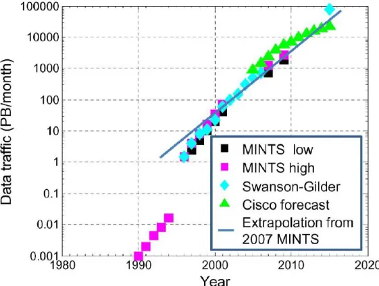
The global data trac is steadly growing [4, 5, 6, 7]. This massive trac is generated by enterprises, governments, universities and individuals. In the last decade, the rapid diusion of cloud computing for data storage, entertainment and social media, signicantly contributed to the increasing demand of bandwidth for data transmission and computing. A feeling on the orders of mangnitude involved can be get by looking at Fig.1.1, which shows the North American internet trac during the last three decades.
Figure 1.1: Amount of internet trac in the North America in the last three decades. 1P B = 1015 bytes.
Datas taken from [7].
All data sources, among which the inuential Minnesota Internet Trac Study (MINTS), show very similar trends. The linear projection extrapolated from the MINT data of2007has been respected during the years:
from a data trac of103P B/monthin 2007, it was reached a volume of104P B/monthin2016. Following
this extrapolation, the projection for 2020 are of 105P B/month. Needless to say, this rapid growth was
link. Nowadays, long haul connections, ranging from tens to hundreds of kilometers, are based on optical bers. Since the early 1970s, the system capacity, i.e., the maximum amount of bits that can be sent in
one second in a single ber, has improved by a factor of105 [7]. On one side, this has been possible by the
introduction of Wavelength Division Multiplexing (WDM) at the beginning of the 1990s, which consists in
the encoding data streams in dierent wavelengths which simultaneously travel along the same ber without interference [12]. WDM improved the aggregate bitrate by a factor of 103 [7] On the other side, also the
spectral eciency (SE), i.e., the number of bits per second per channel bandwidth (typically measured in
b/s/Hz), increased by a factor102[7]. These trends are shown in Fig.1.2.
a)
b)
Figure 1.2: (a) Fiber system capacity during the years. Blue circles represent single mode bers for Time Division Multiplexing (TDM), while red rectangles represent bers engineered for WDM applications. Picture from [7]. (b) Spectral eciency (SE) of a single ber as a function of the years. The red star corresponds to the maximum SE according to Shannon's limit, which is set by the nonlinear eects occurring in optical bers [7]. Picture taken from [7].
Progress in the fabrication technology of optical bers has been of paramount importance as well. There has been a continuous eort in material science to realize low loss optical bers. Since their introduction in the early 1960s, when signal attenuation exceeded1000dBkm−1, losses have been constantly decreased to less
than0.2dBkm−1at a wavelength of1.55µm[2]. The simultaneous reduction of the modal birifrangence and
the engineering of the chromatic dispersion to tailor the group velocity dispersion contributed to increase the bitrate, to improve the signal integrity and to decrease the numbers of repeaters. The hardware which handles the microelectronic interfaces of the transceiving stations has followed similar progress during those years. In this technological challenge, a key role has been played by Very Large Scale Integration (VLSI), that is the continuos reduction of the size of the electronic and optical components. Smaller dimensions imply higher component density and enhanced computing capabilities. This concept is well exemplied by the famous Moore's law, introduced for the rst time in1965, and which states that the number of functions
Year
T
ransistor nu
mber
per chip
Figure 1.3: Transistor count in processors during the years. The solid black curve represent the Moore's prediction of1965. Picture taken from [14].
As reported in Fig.1.4, the gate width of the transistor was approximately 1.3µm wide at the beginning of
the1970s, and stacked to a constant value of ∼25nmduring the last few years. Recent reports show that
15nmtransistors are being implemented in low power microprocessor for smartphone applications.
Figure 1.4: The evolution of the gate length of a transistor during the years. Picture taken from [15].
machines built by a variety of commercial companies, it would be dicult for the industry to advance, since in many cases it would not be ideal for one company to introduce a new product if the other needed machines are not available around at the same time. A shared roadmap to plan and control the technological needs of IC production and to anticipate the evolution of the market was needed. This task has been fullled by the institution of the IndustrialTechnology Roadmap for Semiconductors (ITRS), a set of documents produced by a group of semiconductor industry experts [17].
By the way, the continuos race toward more complex and performant architectures, which shall meet the increasing demand in computation, data trac, bandwidth and storage, hardly will follow the Moore's law in the very near future, if a new paradigm will not support or even replace the one of miniaturization. Indeed, the density of the electrical components has reached a so high level of packaging and integration that the operation frequency of a single processing unit has levelled to few GHz over the last decade. This was due
to heat dissipation, signal attenuation and Resistor-Capacitance (RC) delays associated to the copper lines used for the interconnections [18, 19]. Heat dissipation occurs because the metals have a nite resistance, which increases as the cross section diminuishes. Large scale integration implies an increased number of wires, with smaller dimensions, which goes in the opposite direction with respect to heat reduction . Energy is also required every time that a capacity, which can be associated to a transistor or to a connection line of similar length (these are almost the same and equal to≈1f F for state of the art electronic design and
fabrication [18]), has to be charged or discarged. On average, the switching of a transistor, which can be roughly assimilated to the processing of one bit, consumes about 1pJ of energy [18]. The trends in heat
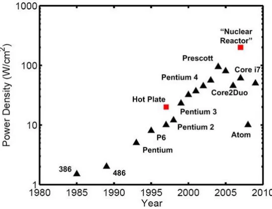
dissipation over the last three decades are shown in Fig.1.5.
Figure 1.5: Power density developed inside a single core microprocessor during the years. Picture taken from [19].
The dielectric support where the ICs are fabricated, which has a poor heat conduction, sets a threshold to the maximum dissipated power density slightly above 100W cm−1. If one thinks that200W cm−1 is the power
generated by a nuclear reactor, it can be seen that this is a huge amount of power. Power loss is also induced by radio frequency (RF) signals which are radiated from the interconnection lines when they operate atGHz
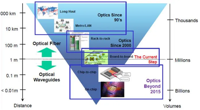
wire does not alter its RC constant [18]. By looking at Fig.1.3, one may wonder how it has been possible to follow the Moore's law in the last decade, if miniaturization suers for all the problems cited above. The answer relies in the introduction of the multi-core paradigm. Instead of increasing the processing capability of a single CPU, many of them, called cores, have been connected together in a single microprocessor and made to work in parallel to increase the overall computational power. By the way, as a natural consequence of coworking, more and more interconnections are needed to let the cores to communicate and exchange data, with the consequence that this approach will soon face the same heat dissipation problems encountered in single CPU units. The only viable solution is the use of optical interconnections instead of copper wires [21, 22, 8, 5, 11, 6]. This is not a completely new paradigm, since it has been already applied at the macro-scale level with the introduction of optical bers for long and medium distance telecommunications. As exemplied in Fig.1.6, in the last20years, copper cables were progressively replaced by optical links.
Figure 1.6: The progressive replacement of copper interconnection with optical ones as the length scale of the communication link decreases. Picture taken from [23].
The length scale of interconnections progressively moved from long haul (>100km), to rack-to-rack (100m)
and even to board to board (<1m) connections. The challenge of the next few years will be the
implemen-tation of optical interconnections at the chip-to-chip (<1cm)or even intra-chip (<10µm) scale. There are
of the nanophotonic wires allows also to eliminate the RC time constant required to shift from an O to an On state and vice versa. In the optical domain, the fundamental limit to the maximum achievable bitrate is the Nyquist limit, which however is very far from being reached, as it lies in the hundreds of T Hz regime.
Photonic chips are also immune to electromagnetic interference and do not suer from antenna's eects. The most promising platform for on chip optical interconnections is Silicon Photonics [24, 25, 21, 26]. The latter is the technology of integrating electronic and photonic functionalities with processing tools currently used in the microelectronic industry. Silicon Photonics is fabbricated by the well-developed infrastructure of Complementary Metal Oxide Semiconductor (CMOS) technology, which allows for VLSI in a cost-eective and monolithic manner. Silicon Photonics started in the1980s, with the pioneering works of R. Soref et. al.
At that time, the rst structures for guiding and splitting light on Silicon waveguides have been proposed and demonstrated [27]. In 1993, following the early ideas of Abstreiter about an OptoElectronic Integrated
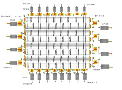
Circuit (OEIC) [28], Soref proposed the concept of superchip [29]. That visionary idea, whose original sketch is shown in Fig.1.7, was incredibly close to the state of the art Optical Networks On Chip (ONoC) produced today.
Figure 1.7: The idea of optoelectronic superchip proposed by Soref in1993. Picture taken from [29].
The idea of Soref was to realize a chip which merges and combines the potential of electronics and photonics on the same substrate, which is the Silicon platform. In the superchip of Fig.1.7, it is possible to recognize all the fundamentals building blocks which are now part of a typical ONoC: etched V-grooves for on chip ber coupling, splitters, combiners, ampliers and modulators, switches, photodiodes and so on. The ten years following1993were not of such big impact for Silicon Photonics as the last ten years. The scene of integrated
photonic devices was dominated by semiconductors belonging to the III-V groups like AlGaAs/GaAs and
InGaAsP/InP. The main reason was that the III-V platform was already well understood for the realization
of active devices like Light Emitting Diodes (LEDs), ampliers or lasers . Silicon, being an indirect bandgap material, has an intrinsic low radiative recombination probability, which makes it not suitable for the fabri-cation of active sources [30]. What is also relevant is that Silicon is a centrosymmetric material, therefore it lacks of the electro optic eect, which is at the basis for the realization of fast electro optic modulators [31]. During those years, it was thought that these fundamental limitations would never promote Silicon as the primary material for the realization of opoelectronic devices. However, already in 1993, Soref stated
counterparts. The multi-billion dollar Silicon VLSI industry has given an immense knowledge of how process silicon circuits at low cost. Much of that know-how can be adapted for optoelectronic processing, putting us part-way up to the learning curse of Silicon optoelectronics [30]. The Soref's predictions were right. The year
2004represented a turning point for Silicon Photonics. A ramping up of the investments to promote research
and developement has been done by governments and industries [30]. A big eort was done by the DARPA microelectronics technology oce with the four year project on electronic and photonic integrated circuits (EPIC) in Silicon at 1.55µm. On the other side, Europe lauched the MELARI initiative at the end of the
1990s, which founded several projects on Silicon Photonics (PICMOS, WADIMOS, SYNERGIA, HELIOS).
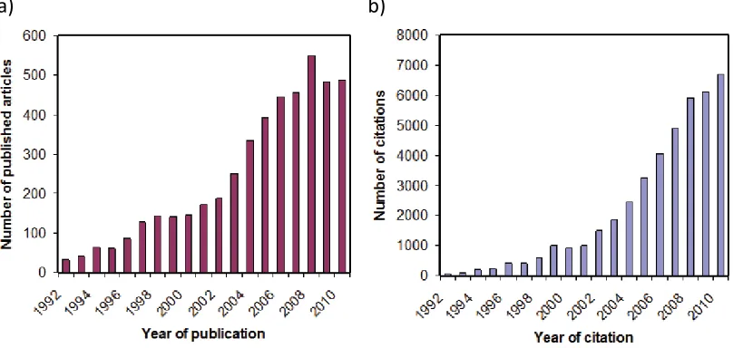
Starting from2004, the path of Silicon Photonics never stopped, as it is witnessed by the steadily increasing
number of publications and citations over the years [22](see Fig.1.8).
a)
b)
Figure 1.8: (a) Number of published articles per year having as a keyword Silicon or waveguide . (b) Number of citations per year to articles having as a keyword Silicon and waveguides. Picture taken from [22].
Years
Micr
oelec
tr
onics
Silic
on
Pho
tonis
Years
Fundamental blocks
Chip
Processing units
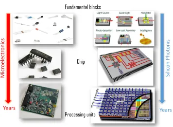
Figure 1.9: The similar path followed by Silicon Photonics with respect to microelectronics during the years. From the basic building blocks, progressively more complex circuits have been realized by connecting together several components.
At rst, the basic bulding blocks have been demonstrated and progressively optimized. These includes both passive devices, as waveguides, splitters, grating couplers and interferometers, and active ones, like modulators, hybrid lasers and photodetectors. Then, these building blocks have been connected together, and assembled in networks to realize more complex functions. As a last step, photonic networks have been compatibily integrated with electronic ones to realize optoelectronic circuits. All these steps have been done under the same paradigms which moves the IC industry: miniaturization and standardization. The latter can be dened as the attempt to realize all the functionalities using only a limited number of materials (mainly Silicon and Silica, but also other group IV compounds and metals) and only one processing technology, which is CMOS. In particular, the CMOS processing technique was already available to Silicon Photonics for low-cost mass production, so no investments were required. With the introduction of Silicon On Insulator (SOI) wafers in the late 1980's and in the middle of 1990's to decrease the parasitic capacitance of ICs,
the index contrast between the core and the cladding material increased, shrinking the dimensions of the photonic devices [32] . The rst waveguides were fabricated in Silicon on heavily doped Silicon, with poor refractive index contrast, of the order of0.01−0.1[27, 33]. The guided modes were weakly conned within
the waveguide, with considerable energy leakage into the substrate. Large radius (>100µm) was required to
bend the waveguides without signicant radiative losses. The use of SOI wafers permitted to use Silica as the cladding material, boosting the refractive index contrast to ≈2.92 at a wavelength of1.55µm. As a result,
modes are more conned, and waveguides can be bent with lower radii [34]. The shift from the850nmband
to the O-band(1.26µm−1.36µm)and C-band(1.53µm−1.565µm) for ber-optics communication; which
neural networs [40, 41, 42] and so on. Today, Silicon Photonics can be considered as a mature technology, which is the subject of many books [25, 24] and enstablished international conferences [43, 44]. ONoC moved from the laboratories to the market, which is projected to increase from US$-25M in 2013 to more than
US$-700M in 2024[23]. Fig.1.10 reports an example of a commercial device fabbricated by Intel labs and
named the Silicon Photonic link [45].
a)
b)
Figure 1.10: (a) The Silicon photonic link developed by Intel. (b) Schematic of the operation of the Silicon Photonic link. Pictures taken from [46].
It is a transceiver which operates at50Gbpsusing4hybrid Silicon laser sources which fed a WDM stage and
are coupled to a ber link. It has been launched on the market in 2015. Another example, which outlines
Figure 1.11: A schematic of the layout of the transponder aggregator developed within the european project IRIS. Picture taken from [47].
If successfully demonstrated in 2016, the router will pave the way for a new generation of optical systems
integrated in a single chip (more than105photonic components and 48WDM channels in less than30mm2
of chip area). Such a chip will enable network operators to enhance the network performance, increasing node capacity as required by future 5G networks and Cloud.
Some challenges are, however, still open. As already introduced before, Silicon is mainly a passive material due to its indirect bandgap, and the realization of active devices still mainly proceed through the hetero-integration of III-V semiconductors [48]. These processes are expensive and not always compatible with the CMOS fabrication. Monolithic integration would be desired, but still much work has to be done in this direction. The same does not hold for photodetectors at 1.55µm. Silicon is transparent in the O and C
1.1 Silicon photonics building blocks
In the next sections, the main building blocks of a Silicon Photonic network are introduced and briefely re-viewed. The rst block which will be presented is the waveguide, then couplers and splitters will be discussed. Next, more advanced devices will be reported, like optical resonators, sequence of coupled resonators, electro optic modulators and active sources.
1.1.1 Waveguides
Waveguides are probably the most important elements of photonic networks, since they carry the optical signal from one block to the other. Light is conned inside the waveguide by Total Internal Reection (TIR), which requires a cladding material of lower refractive index than the one of the core, as shown in Fig.1.12(a). Light travels in the form of discrete modes of electric eld prole em(x, y, ω), which are solution of the Helmoltz equation [51]:
∇2
xy+βm2
em(x, y, ω) =
ω2
c2n
2(x, y)e
m(x, y) (1.1)
𝑧
𝑥 𝑦
𝑛
𝑐𝑙𝑎𝑑𝑛
𝑐𝑜𝑟𝑒TIR
a)
b)
TE modes
TM modes
𝑥 𝑦
E
x,y1
0
-1
Figure 1.12: (a) Schematic of a channel waveguide. The index of refraction of the cladding material isnclad while the one of the core isncore.The propagation direction is z. (b) Distribution of the dominant electric eld component (Ex for TE modes,Ey for TM modes) for the three lowest order TE and TM modes of a waveguide with cross section1.6µm×0.25µm.
Due to the invariance of the refractive index distribution n(x, y) along the propagation direction z, the
dependence on this coordinate is on the forme−iβmz, whereβ
m= ωcnef f,m is called the modal propagation constant (or wavevector), and nef f,m the eective index. In general, nef f,m is a complex quantity. As for plane waves, the real part is associated with propagation, while the imaginary one to losses. The eld intensity exponentially decreases along zas e−αz, where the attenuation coecientαis given by α= 2ω
c Im(nef f,m). Fig.1.12(b) shows an example of the electric eld distribution em(x, y) for three lowest order solutions of Eq.1.1. Each solution is associated to a dierent number of nodal pointsn, in which the electric eld is equal
to zero. In what follows, the modal ordermwill be dened asm=n+ 1. As the modal order increases, the
modal connenement, dened as:
Γm= ´
wgn
2(x, y)|e
m(x, y)|2dxdy ´
n2(x, y)|e
m(x, y)|2dxdy
(1.2)
the refractive index of the core. Given the geometry of the waveguide, the maximum number of supported modes is limited. Apart from very simple geometries, as the slab one [52], no analytical expression exists for determining this number. For the channel waveguides implemented in this work, it is possible to take as a rough rule the fact that light of wavelength λ can not be conned to features which are lower than
λ
2 due to the diraction limit. The maximum number of supported modes (for a xed polarization) can
then be approximated as ∼4wh
λ2 . Modes can be classied also on the basis of their polarization. In general, for waveguides of sub-wavelength dimension, the electric and the magnetic elds are not transverse to the propagation direction and neither orthogonal to each other. The classication between Transverse Electric (TE) and Transverse Magnetic (TM) modes is done on the basis of their dominant electric feld component, which for the reference frame of Fig.1.12(b) concides with the xdirection in case of TE modes, and y for
TM modes. The eective index of each mode depends on wavelength. As the latter increases, the mode get less conned due to diraction, and the eective index decreases. The way this occurs strongly depends on the mode order, the waveguide geometry, the polarization and the core and cladding chromatic dispersion. In micron size waveguides, it is the geometric dispersion which dominates over chromatic one, in opposition with what happens in an optical ber [2, 53]. A measure of the eective index dispersion is given by the high order dispersion coecientsβm(j)= d
jβ
m
djλ . Forj= 1, this is given by:
β(1)m =
dβm
dλ =
nef f,m−λ
dnef f,m
dλ
1
c =
ng,m
c (1.3)
and represents the inverse of the group velocity vg,m = nc
g,m, where the group index is dened asng,m = nef f,m−λ
dnef f,m
dλ . Forj = 2, the quantityβ
(2)
m is called Group Velocity Dispersion (GVD), and forj >2 the terms are in general referred as jthorder dispersions. Another important property is the mode eective
area Aef f,m, dened as:
Aef f,m= ´
|em(x, y)|2dxdy
2
´
|em(x, y)|4dxdy (1.4) which is a measure of the eective extension of the optical mode into the core and cladding regions. Higher order modes, being less conned, have larger eective areas than the lower order ones.
The rst Silicon waveguides, reported in1980, were fabricated on the Silicon-On-Silicon platform, in which
the crystalline Silicon core was deposited on a substrate of heavily doped one. The process of doping lowers the index of refraction of the material through plasma carrier dispersion, thus creating the conditions for waveguiding [33]. However, the index contrast was of the order of 0.01, so the mode was highly delocalized
and suered from leakage of energy into the substrate. In the late 1980s, SOI wafers were introduced in
the microelectronic industry, oering an improved refractive index contrast. Wafers were developed with methods like SIMOX, BESOI and SmartCut [24]. Waveguide fabrication requires denition of their edges in a photoresist (through deep UltraViolet (DUV) or electron beam lithography) and subsequent dry etch. The process naturally introduces roughness on the side walls of the waveguide, which is source of scattering. As a consequence of the enhanced refractive index contrast, the spatial mode prole got tightly conned inside the core. On one side, this allowed to shrink the waveguide dimensions and to realize smaller bends, and on the other side to avoid energy leakage into the cladding material. The rst fabricated SOI waveguide was characterized by0.5dBcm−1 of propagation loss, but this was due to the fact that it had several microns of
(LOCOS), a technique rstly reported at the Carleton University, allowed to realize etchless ridge Silicon waveguides by the local oxydation of Silicon, which resulted in0.3dBcm−1of propagation loss in a1µmwide
waveguide with a rib height of70nm[55]. For small scale production, the use of electron beam lithography
has proven to be a very eective tool for the realization of low loss Silicon waveguides. For example, Gnan et. al. reported about photonic wires formed by electron beam lithography with 0.92dBcm−1 of loss [56].
The current record of propagation loss at1.55µmis0.27dBcm−1, achieved by Bogaerts and Selvaraja using
hybrid ridge-channel waveguides [57].
1.1.2 Couplers
One of the biggest challenges in realizing photonic chips relates to the eciency of the coupling of light in the waveguide by an input ber. The diculties arise from the huge mismatch between the eective area of the mode which propagates in the ber and the one in the waveguide. A standard single mode Silica ber has a core with a typical dimension of ∼ 10µm, and an eective mode area of ∼ 315µm2, while the one
of a waveguide is of the order of 1µm2, which is more than two orders of magnitude lower. It comes out
that if the two cores are brought into contact (edge coupling), more than 20dB of power is lost. Tapered
lensed bers, which are bers in which one of the two ends are progressively reduced in size to∼2µm, oer
better performances by focusing light to an eective area of∼10µm2, thus reducing the coupling losses at a
value close to10dB. If lower losses are needed, the input facet of the waveguide havs to be engineered. Two
approaches have been developed during the years: tapering, which consists in enlarging or reducing the size of the waveguide core as it approaches to the ber, or patterning subwavelength periodic structures at the waveguide extremities called grating coupler. Both are schematically shown in Fig.1.13.
a)
b)
c)
Direct tapering
Inverse tapering
Grating coupler
Fiber
𝜃
Fiber
Fiber
Figure 1.13: (a) Direct tapering of a waveguide. (b) Inverse tapering of a waveguide. (c) Grating coupler, with the ber tilted by an angleθ with respect to the normal of the grating. In all panels, the yellow circle
sketches the modal intensity of the propagating light. Fiber is not to scale.
Tapers are also called Spot Size Converters (SSC). Tapering can be direct if the end of the waveguide is smoothly increased to match the dimension of the spot of the ber, or inverse, if the end of the waveguide is progressively reduced to delocalize the modal prole outside the core. The performances are quite similar. By using direct tapering, in which both the width and the thickness of the waveguide were increased, Day et. al. demonstrated coupling losses of less than0.5dBin1mmof taper length [58]. M.Pu et. al. reported on inverse
tapers in which a 450nm width waveguide was reduced to only 15nm using thermal oxydation, achieving
an ultra low value of 0.36dB of coupling loss [59]. Grating couplers relies instead on a completely dierent
etched with a period Λ, creating alternating regions of dierent index of refraction. As a consequence of
the periodicity, the mode of propagation constant β is converted into a wave which is diracted into the
cladding with an angle θwith respect to the propagation direction [60]. This occurs if the periodΛ satises
the following phase matching relation:
sinθ=Λnef f−λ0
Λn (1.5)
wherenef f is the eective index of the mode which diracts light,λ0is the wavelength andnis the refractive
index of the medium in which the wave is radiated. A ber placed at an angleθcan than collect the diracted
light. The reverse process can be exploited to couple light from the ber into the mode of the waveguide. Starting from the most simple implementation described above, the eort to reduce the coupling losses in grating couplers produced a wide variety of structures. Coupling eciencies of37%have been demonstrated
using shallow-etched gratings [61], 42%using photonic crystal structures within the grating [62],64% using
apodization [63], and 69% using backside reectors [64]. The current record of couplig losses is 0.58dB,
achieved by Ding et. al. in a fully etched apodized grating coupler using sub-wavelength photonic crystals and a bonded aluminum mirror [65].
1.1.3 Splitters and combiners
Light which propagates in a waveguide can be split into one or more waveguides and vice-versa. Several structures allow achieving this: Y-junctions [66], Multi Mode Interference (MMI) devices [67] and directional couplers [68]. Only the latter will be briefely discussed here, due to its use in the designs shown in the rest of this thesis. As sketched in Fig.1.14(a), a directional coupler if formed by two waveguides which are brought in close proximity. Their separation is the coupling gapcg,which is few hundreds of nanometers long [51]. The region where the two waveguides are close is longL.
𝑐
𝑔𝐿
𝑧 𝑦 𝑥
𝐸
𝑖𝑛,1𝐸
𝑖𝑛,2𝐸
𝑜𝑢𝑡,2𝐸
𝑜𝑢𝑡,1a)
b)
E
x1
0
-1
Even TE
Odd TE
x=0
Figure 1.14: (a) Sktech of a directional coupler of lengthLand coupling gapcg. Electric eldsEin,1andEin,2
represent the inputs, while Eout,1 and Eout,2 represent the outputs. (b) Dominant electric eld component
(Ex) for the even and odd TE supermodes of the two coupled waveguides.
The gap is so narrow that the evanescent tail of the optical mode of each waveguide penetrates, through the cladding, into the core of the neighboring one, thus allowing cross talk between the two. In the most simple case of two identical parallel waveguides, if some power P10 is launched into waveguide1 while waveguide2
P1(L) =P10cos2
π
2 ·
L
Lc
=|r|2P
10 (1.6)
P2(L) =P10sin2
π
2 ·
L
Lc
=|κ|2P
10 (1.7)
where r and κare called the reection and the transmission coecient of the coupler respectively. κ and r for a lossless system satisfy |r|2+|κ|2 = 1. In Eqs.1.6-1.7, the quantity L
c is called the transfer length, and coincides with the length of the coupler which realizes a complete transfer of power from waveguide1to
waveguide 2. It can be demonstrated thatLc is given by [52]:
Lc=
λ
2(no−ne) (1.8)
wherenoandneare the eective indexes of the supermodes of the combined structures, shown in Fig.1.14(b). The subscripts o and e stand for odd and even respectively, and refer to the parity of the electric eld
distribution with respect to thex= 0axes of Fig.1.14(b). In general, if both waveguide 1and waveguide2
are excited at the input, the system is described by a 2×2unitary matrixM which maps the input electric
eld vector Ein= (Ein,1, Ein,2)at z= 0 into the output oneEout = (Eout,1, Eout,2)at z =L. The matrix M is given by:
M = r −iκ
−iκ r
!
e−iβL (1.9)
where β is the propagation constant of the mode in the waveguides, whileκand rare dened above. If the
two waveguides are not equal, and hence a phase mismatch∆βexists between the propagation constants, the
expression for the transfer matrix M gets more complex. When∆β 6= 0, a complete power transfer can no
more occur between the two waveguides [51]. Directional couplers are fabricated through patterning of the photoresist and subsequent etching. Coupling gaps as low as 160nmcan be fabricated using193nm DUV
lithography and dry etching. For lower gaps, electron beam lithography gives better results. The size of the gap is a critical dimension for the coupler, since the dependence of the coupling and reection coecients on the gap is exponential [69]. This is a direct consequence of the fact that the evanescent tail of the optical modes exponentially decreases in the cladding. The ability to fabricate waveguides with tight tolerances on the dimensions is also required to set the phase mismatch ∆β equal to zero, thus allowing a more ecient
energy transfer. For these reasons, tapered directional couplers have been proposed, in which the size of one waveguide is intentionally adiabatically swept in the neighboring of the nominal one. This trick allows to relax the fabrication tolerances on the nal waveguide dimensions to tens of nanometers [70, 71].
1.1.4 Microresonators
c)
a)
b)
d)
Figure 1.15: (a) Scanning Electron Microscopy (SEM) image of a ring resonator in the All Pass conguration. Picture taken from [76]. (b) Optical microscope image of a racetrack resonator. Picture taken from [79]. (c) SEM image of a suspendend microdisk resonator. Picture from [75]. (d) SEM image of a suspended microtoroid resonator. Picture taken from [77].
Each of these shapes possess its own advantages and disadvantages, so the resonator type has to be choosen to best match the purposes of the experiment. The common feature of each resonator is that light is made to travel in a closed path, and, as a consequence, only certain wavelengthsλmcan be supported. For travelling wave resonators, as microrings or racetracks, these wavelengths are the ones which satisfy the resonance condition [74]:
nef fp=mλm (1.10)
wherenef f is the eective index of the waveguide,pis the resonator perimeter andmis an integer number. Eq.1.10 has a simple physical interpretation: the perimeter of the resonator has to contain an integer number of wavelengths (in the material), in such a way that the travelling wave, after a roundtrip, can reproduce itself. Alternatively, Eq.1.10 can be cast in the form βp = 2mπ, in which β is the propagation constant
dened in Section 1.1.1. Given in this form, the resonance condition is met every time that after a complete roundtrip, the light has acquired a phase which is a multiple integer of 2π, so that the wave undergoes
constructive interference each time it completes a roundtrip.
1.1.4.1 Add Drop and All Pass congurations
a)
b)
𝐸
𝑖𝑛𝐸
𝑜𝑢𝑡𝜏
(𝑟, 𝜅)𝐸
𝑖𝑛𝐸
𝑇𝐸
𝐷𝐴
𝑑𝑑 (𝑟, 𝜅) (𝑟, 𝜅)𝜏
𝐹𝑃𝑅 𝐹𝑃𝑅 CouplingFigure 1.16: (a) Ring resonator in the All Pass conguration. The coupling region and the Free Propagation Region (FPR) are explicitally indicated. The reection and transmission coecients of the coupler arerand κrespectively. Scattering losses are indicated asτ. (b) Ring resonator in the Add Drop conguration. The
meaning of the parameters are the same as for panel (a).
The electric eld amplitude at the input port Ein is connected to the one at the output port Eout by the transfer functionHAP(ω), which is a complex function that depends on the light frequencyω. An expression forHAP(ω)can be derived using the Transfer Matrix Method (TMM) [80]: the two sections of the resonator, which are the coupling region CR and the free propagation region FPR in Fig.1.16(a), are treated as four and two port systems respectively, whose outputs are connected to the inputs by linear matrix relations. A system of equations is then derived which can be solved for Eout, once thatEin is known. The transfer functionHAP(ω)can be demonstrated to be [81, 80]:
HAP(ω) =
τ−re−iφ(ω)
rτ−e−iφ(ω) (1.11)
where τ = e−αp (α is the scattering loss coecient) represents the roundtrip losses, r is the reection coecient of the coupler and φ(ω) = ωcnef f(ω)pis the roundtrip phase. The quantity |HAP(ω)|2 is plotted in Fig.1.17 as a function ofφ.
?/2:
-1.5 -1 -0.5 0 0.5 1 1.5
|H AP | 2 0 0.2 0.4 0.6 0.8 1
= = 1
= = 0.95
= = 0.8
?/2:
-2 -1 0 1 2
|H D AD | 2 0 0.1 0.2 0.3 0.4 0.5 |H T AD | 2 0 0.2 0.4 0.6 0.8 1
= = 0.95
= = 0.95
As already introduced above, each time that φ= 2mπ, the resonance condition is met, and a transmission
dip appears in the spectral response. When this occur, energy is accumulated inside the resonator and a fraction τ is lost (for example, from scattering with the side walls roughness), resulting in a lack of power
in the transmission. Outside the resonance condition, the resonator behaves as a straight waveguide, and no light is coupled. It is worth to note that whenτ = 1, i.e., no losses are present, HAP = 1independently on the phase. This comes directly from energy conservation.
The AD resonator has instead two input ports, conventionally named Input and Add, and two output ones, named Drop and Through. These are sketched in Fig.1.16(b). If only the Input port is excited, the transfer functionHD
AD(ω), which express the ratio between the input eldEinand the dropped eldED, is given by [81]:
HADD (ω) =
κ2√τ eiφ(ω)/2
r2τ−eiφ(ω) (1.12)
whereκis the transmission coecient of the coupler (for simplicity, the two coupling regions are assumed to
be symmetric). The transfer function of the Through port HADT (ω) = ET
Ein is instead given by [81]:
HADT (ω) = r e
iφ(ω)−τ
eiφ(ω)−r2τ (1.13)
The quantities |HT
AD(ω)|2 and |HADD (ω)|2 are plotted in Fig.1.17 as a function of φ(ω). As for the AP conguration, everytime that φ= 2mπa resonance occurs, which is manifested in a peak in the Drop signal
and in a dip in the Through one. When the Add port is simultaneously excited, it is possible to exploit the linearity of the system to calculate the expressions for the dropped and transmitted powers. The key parameters which characterize a resonator are the quality factor Q, the Free Spectral range (FSR) and the Field Enhancement factor FE. The quality factor of themthresonance order is dened as the ratio between the resonant wavelength λm and the Full Width at Half Maximum (FWHM)∆λmof the peak, i.e., Q= ∆λλmm. It can be shown, by expanding the exponential terms in Eq.1.12 to the rst order in ω−ωm (ωm is the resonance frequency), that the the peak is actually a lorentzian function. The FSR is dened as the distance between two adjacent resonance wavelengths, while the FE factor is the ratio between the eld inside the resonator and the one in the input waveguide. The expressions for these quantities are reported in Table 1.1. The interested reader can refer, for example, to Ref.[82], for a complete derivation.
Parameter All Pass Add Drop Q πng(λm)p
√ rτ
(1−rτ)λm
πng(λm)pr
√ τ
(1−r2τ)λm
FSR λ2m
ng(λm)p
λ2m ng(λm)p
FE iκ
1−rτ e−iφ(ω)
iκ
1−r2τ e−iφ(ω)
Table 1.1: Main parameters which characterize the performances of a resonator expressed as a function of the coupler parameters randκ, the perimeterp, the resonant wavelengthλmand the group indexng.
By looking at Table 1.1, some general considerations can be made:
The quality factor is inversely proportional to the transmittance of the couplerκand to the roundtrip
losses τ. Hence, high Q resonators are characterized by weak coupling with the waveguide and low
losses.
For small losses, the on resonance FE is given byF E∼1/κ. Hence, if the resonator is weakly coupled
to the waveguide, and has very low losses, the eld inside the resonator is greately enhanced with respect to the one in the bus waveguide. For example, ifκ2= 0.01, the power inside the resonator is
100times higher than in the bus waveguide. As described later and in Chapter 6, this feature can be
exploited for nonlinear optics applications.
Another important quantity is the group delay τg. The latter is dened as the derivative of the phaseδ(ω) of the transfer function with respect to the frequency, i.e.,τg =dδdω(ω). As derived in Chapter 6, it represents the time delay that is imparted to an incoming electric eld envelope when passing through the resonator. Fig.1.18(left panel) shows the phaseδfor an AP lter in the neighboring of a resonance.
?/2:
-0.3 -0.2 -0.1 0 0.1 0.2 0.3
/
/2
:
(rad)
0 0.1 0.2 0.3 0.4 0.5 0.6 0.7 0.8 0.9 1
?/2:
-0.3 -0.2 -0.1 0 0.1 0.2 0.3
=g
(ps)
-6 -5 -4 -3 -2 -1 0
Figure 1.18: Left: Phaseδof the transfer functionHAP as a function of the roundtrip phaseφ. Right: group delay τg as a function of the rountrip phase φ. The parameters used in the simulation are the ones of the All Pass lters implemented in the delay line for the broadband design of Section 6.4, which are reported in Table 6.2.
As it can be appreciated, the curve is very steep in proximity of the resonance, which means that the group delay is quite high in this region. The derived group delay is shown in Fig.1.18(right panel). The slow light properties of the resonator can be more appreciated through an example. As shown in Fig.1.18(right panel), if the carrier frequency of the incoming eld lies near resonance, delays at the order of∼6pscan be
achieved. The size of the resonator used for this simulation is50µm. If the resonator would be replaced by
a straight waveguide of group velocityvg = 75µmps (a waveguide of cross section400nm×250nmfullls this requirement) and having the same length, the group delay would be τg= 5075 ∼0.75ps, i.e,8times shorter.
The speed of light is then reduced by a factor8 by using the resonator.
1.1.4.2 Sequence of coupled resonators: CROW and SCISSOR
The slow light property of single resonators can be enhanced byN times ifN cavities are connected in series
a)
b)
𝐸
𝑖𝑛𝐸
𝑇𝐸
𝐷𝐸
𝑇
𝐸
𝑖𝑛𝐸
𝐷Λ
Unit cell
Figure 1.19: (a) Sketch of a CROW made by5coupled resonators. The input, Drop and Through portsEin,
EDandET are also indicated. (b) Sketch of a SCISSOR made by5side coupled resonators. The input, Drop and Through ports Ein, ED andET are also indicated. The lattice periodicity of the unit cell is indicated byΛ.
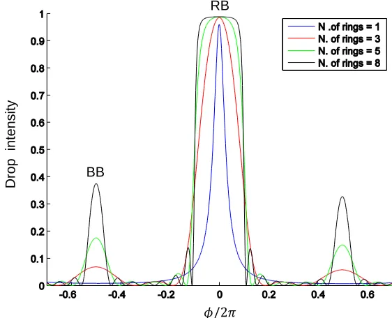
In the CROW geometry, resonators are directly coupled, and only the rst and the latter resonators of the sequence are coupled to the bus waveguides. On the contrary, in the SCISSOR geometry, resonators are all coupled to two straight side waveguides. Due to the implementation of the ring-based SCISSOR geometry in Chapter 2, a brief discussion of its spectral properties is now outlined. The SCISSOR is actually a one dimensional photonic crystal made by the repetition of a unit cell constituted by an AD lter. From the theory of light propagation in periodic media [51, 88], it results that there are some frequency ranges in which light can not penetrate in the structure, which are called Photonic BandGaps (PBG). PBGs manifest themselves in dips in the transmission spectra (Through port) and peaks in reectance (Drop port) spectra. An example of the latter is shown in Fig.1.20.
Drop
intensity
𝜙/2𝜋
RB
BB
The SCISSOR conguration has two types of PBGs, one is called the Resonator Band (RB) and the other the Bragg Band (BB) [78]. The RB is due to the response of each resonator of the chain. Indeed, it occurs when the input wavelength satises the condition in Eq.1.10. The BB is due to the coherent, constructive superposition, of all waves which are back reected by each resonator. Infact, even when the input wavelength is o resonance, a small portion of electric eld is coupled into the Drop port (back reected). If the resonator distance Λ satises Λβ = qπ, in which q is an integer number, then all the reected waves superimpose
contructively, and signicant power can be build up into the drop port. If the SCISSOR is designed to have
Λ =πR, in which R is the radius of the rings, the RB and the BB overlap for all orders. From Fig.1.20, it
is possible to notice that as the number of resonators increase, the bandwith of the lter both attens and increases, becoming very similar to a box-like response. One may wonder what happens if the resonators which compose the sequence are not all equal, i.e., they have resonant frequencies which are slightly detuned between each other. This situation can be intentionally induced already at the design stage [87], or it can be an undesired consequence of defects in the fabrication process [89]. What happens is that defect states, in which the energy is mosty localized in the neighborhood of the defects, are created. These manifest in the spectral response as narrow transparency peaks inside the PBGs of the Through port, or equivalently in dips into the Drop one. The phenomenon is called Coupled Resonator Induced Transparency (CRIT) and is widely discussed in Refs.[87, 78, 82]. By virtue of the intrinsic link between CRIT and defects, a device which quanties the amount of fabrication disorder in a SOI wafer by exploiting the CRIT eect has been proposed [89].
1.1.4.3 Tuning of microresonators
The resonance wavelength of a microresonator is very sensitive to fabrication imperfections. By dierentiat-ing both sides of Eq.1.10, it is derived that a small change in the eective index∆nis reected in a shift in
the resonance wavelength of ∆λ=λm∆ngn. For example, a variation of5nmin the width of a waveguide of cross section450nm×250nm, which corresponds to a realistic value for both DUV and electron beam
lithog-raphy [90, 91], implies ∆n∼0.01(calculated from a Finite Element Method simulation), and a consequent
wavelength shift of∆λ∼3.8nm(in the calculation,λm= 1550nmandng∼4). For resonators implemented in WDM applications, this quantity is typically much higher than the FWHM of the resonace [74], with the consequence that if the lter is designed to drop all the power at λm, no power will be actually dropped when fabricated. It comes naturally that a trimming mechanism is required for aligning the resonance at the wavelength where the lter has been designed to operate. Two tuning mechanisms are typically implemented: thermal [92, 93] and plasma carrier tuning [94, 95]. The rst exploits the thermo optic coecient of Silicon, which is dn
dT = 1.86·10
−4K−1 [96], to change the eective index of the mode by inducing a temperature
variation of∆T into the waveguide core. The relation is linear, i.e,∆n= dn
dT∆T. At this purpose, a metallic heater can be placed on top of the resonator, optically isolated from the mode by hundreds of nanometers of cladding. When a current ows in it, the metal increases its temperature, and by conduction the heat ows through the cladding and reaches the waveguide core. For example, for correcting the eective index by0.01,
a temperature increase of the core of the order of ∼ 55K is required, which can be easily achieved using
an Aluminium or a Titanium Nitride (TiN) metal stripe of less than1µm2 of cross section and fewmW of
electrical power [82]. Since the sign of the thermo optic coecient is positive, temperature tuning only acts in one direction. For realizing a wavelength shift in the opposite direction, free carrier injection can be used. When electrons and holes are injected into the Silicon core at concentrations above equilibrium, indicated as
∆N and∆P respectively, both the refractive indexnand the absorption coecientαof the material change.
∆n=σF CDe ∆N+σF CDh ∆P0.8=−8.8·10−22∆N−8.5·10−18∆P0.8 (1.14)
∆α=σF CA(∆N+ ∆P) = 1.45·10−17(∆N+ ∆P) (1.15) In the relations (1.13) and (1.15), the carrier concentrations have been expressed incm−3. For example, to
change the refractive index of0.01, an electron concentration of∆N ∼1019cm−3is required. A wide variety
of geometries have been implemented to achieve this goal. One of the most popular and eective one consists in embedding a rib waveguide into the intrisinc region of a PIN diode, and by connecting thenandpregions
to metal electrodes [98]. In this way, the optical mode propagates without signicant attenuation, because it has negligible overlap with the highly doped regions (which are source of losses, as indicated by Eq.1.15). Thermal and free carrier eects are the most important and more eective tools for tuning the spectral response of resonators. Their main limitation relies on the fact that they are quite slow tuning mechanisms. Thermal eects have a slow dynamics because of the quite high heat capacity of Silicon and the very low thermal conductivity of the Silica cladding. Typically involved timescales lie in the µs range [96, 99]. Free
carriers are limited by the recombination time, which is of the order of 500ps−5nsfor micron size Silicon
waveguides [100, 101, 102], and by the charging and discharging of the junction and diusion capacitances of the PIN diodes [103].
1.1.4.4 Applications of Silicon microresonators
Originally, microresonators have been conceived for WDM applications. The ability to send a specic set of wavelengths into the Drop port make resonators natural building blocks for ltering applications. The characteristics which are required to eciently route dierent channels are a very high FSR, low insertion loss, steep roll o of the transmittance and high extinction. Typical values for C band telecom applications are tens of nanometers for the FSR, ∼0.2dB/GHz for the transmittance roll o, and <−30dB for the extinction
[72]. Usually, these requirements are too high to be fullled by a single resonator, so high order lters like CROWs or SCISSORs are implemented. The reader can refer to Ref.[103]for a state of the art review about this subject. Resonators can be organized in matrix of elements for bidirectional routers. An example is the one by D. Sherwood et. al., who demonstrated a 4×4 nonblocking Silicon optical router using thermo
optic switching, with a footprint of 0.07mm2 [104]. Their design enabled bidirectional communications
among the four input ports and the four output ports. Each communication path demonstrated a maximum extinction of −20.79dB and a bandwidth of38.5GHz.The biggest, and most complex matrix router is the
one developed within the project IRIS, and discussed at the beginning of the chapter, with more than 105
photonic components, 4 directions of operation and 48 WDM channels. Resonators are also the building
blocks of optical modulators (discussed in Section 1.1.5) and laser cavities (discussed in Section 1.1.6). Silicon resonators have been demonstrated to be very eective tools for sensing and biomolecule recog-nition. The optical mode inside the resonator evanescently extends into the cladding, where the target molecule/protein can be trapped by surface functionalization [105, 106]. The mode is then able to sense the external environment, and, as a consequence, its eective index is altered. From Eq.1.10, this implies a shift of the resonant wavelength, which constitutes the transduced signal. The shift is proportional to the amount of biomolecule that is trapped on the surface, so not only the concentration, but also the kinetics of the binding reaction can be tracked [107]. The parameters which quantify the performances of the sensor are the sensitivity and the limit of detection. The sensitivityS is dened as the nanometers of resonance shift as a
measurements of the same blank solution (when no analyte is present). A review on the state of the art of resonators for biosensing is given in Ref. [72].
Due to the ability of optical microresonators to enhance the power which is sent into the input waveguide, a wide variety of nonlinear optical phenomena have been demonstrated. Examples are wavelength conversion through Stimulated Four Wave Mixing (SFWM) [108, 109], optical frequency combs through Spontaneous FWM (sFWM) [110, 111, 112], optical parametric oscillators and ampliers (OPO and OPA) [113, 114, 115]. Some of them are reviewed in Section 1.2. Nonlinearities associated to Two Photon Absorption (TPA) have been used for all optical switching[116, 117]. Thermal eects induced by nonlinear absorption, which drive the resonator into a bistable state, have been proposed for the realization of all optical memories [118]. Dynamical eects induced by the interplay of thermal and free carrier nonlinearities have been demonstrated to produce the self pulsing [96, 119, 120]of the transmitted signal or even chaos [99]. This part will be investigated in depth in Chapter 2.
1.1.5 Modulators
Modulators are used to convert an electrical signal into an optical one and vice versa. Through modulators, it is possible to encode data into the optical signal. Their working principle is depicted in Fig.1.21.
𝐼𝑛
𝑂𝑢𝑡
p-doped
n-doped intrinsic
Wavelength Out
Low
𝜆0
Laser wavelength
Wavelength Out
𝜆0− Δ𝜆
Laser wavelength
High
OFF state
(Reverse bias)
ON state
(Forward bias)
a)
b)
Figure 1.21: (a) Sketch of a ring resonator realized using a rib waveguide which embeds a PIN junction (shown in the inset). The input light is constant, while the output one depends on the bias of the junction. (b) Relative position of the resonant wavelengthλ0and of the input laser wavelength in case of reverse and
forward bias of the PIN junction. In the latter case, the injection of free carriers in the intrinsic region determines a shift of the resonance wavelength of∆λ.
The resonance wavelength of a microresonator, in this example an AP lter, is initially aligned with the carrier wavelength λ0 of the WDM channel that has to be modulated (Fig.1.21(b)). The waveguide which
forms the resonator is embedded into a PIN junction, which can inject carriers into the core when the junction is forward biased. When this occurs, the modal eective index changes through plasma carrier dispersion (see Eq.1.14), and the resonance position accordingly shifts by a quantity∆λ. The carrier wavelength is no
speed and depth, optical bandwidth, insertion loss, area eciency (footprint) and power consumption. An excellent review on the state of the art of optical modulators is given in Ref.[103]. Basically, two big lines of research developed during the years. Both rely on plasma carrier dispersion, but the rst class is based on carrier injection while the other one on carrier depletion. In general, modulators based on carrier injection have a very good extinction (∼ −8dB at maximum operating speed), but low bandwidth (∼ 10GHz).
The speed is mainly limited by the diusion times of the carriers from the highly doped regions into the intrinsic one [103]. On the contraty, modulators based on carrier depletion have poor extinction (∼ −1dB
at maximum operating speed) but high bandwith (∼30GHz). In this class of modulators, the optical mode
propagates in the junction region of a reverse biased PN diode, and the modulation is achieved by changing the depletion width of the juction. The extinction is limited by the amount of carriers which can be depleted between the on and the o states. State of the art modulators based on carrier accumulation are represented by the work of Liao et. al., in which it is reported 10Gbpsoperation with an extinction ration of −3.8dB
[121], and by Lightwire, which achieved the same bandwith but with the improved extinction ratio of−9dB
[122]. The fastest reported Silicon modulators are based on carrier depletion and are the ones of Liu et. al., which operates at 40Gbps [123], and the modulators of T.Baba et. al. [124] and D.Thomson et.al. [125],
with50Gbpsoperation.
1.1.6 Lasers and photodetectors
As introduced at the beginning of Chapter 1, one of the still open questions of Silicon Photonics is the lack of ecient monolithic laser sources, which could be easily integrated using the standard CMOS process ow. In fact, Silicon is a very good passive optical material, but, due its indirect bandgap, it is very inecient for light emission, which are necessarily phonon mediated [25]. Dierent approaches to the problem have been aorded to overcome this intrinsic limitation. One of these is Stimulated Raman Scattering (SRS) [2, 126]. SRS relies on the interaction of photons with the optical phonons inside the material, which is described by the Raman contribution to the third order optical nonlinearity χ(3) of Silicon [127]. A pump wave can be
scattered by an optical phonon into two waves, called Stokes (or signal) and Anti-Stokes (or idler) waves. The spectral separation between the Stokes and the Anti-Stokes wave is determined by the energy and the wavevector of the involved phonon. If a signal wave is added to the pump, and tuned at the Stoke frequency, the material can exhibit a net gain at the idler frequency. By exploting this fact, Raman lasing on Silicon has been demonstrated in2004[128]. Recently, vefold enhancement of the gain has been demonstrated in Silica
waveguides which embeds Silicon nanoparticles [129]. However, lasers based on SRS require intense pump elds, which are naturally subject to TPA and Free Carrier Absorption (FCA) (both discussed in detail in Chapter 2), which are limiting the maximum gain [130]. Other approaches than SRS make use of epitaxial growth of III-V compounds on Silicon. Such materials have a direct bandgap, so they can be electrically pumped to obtain amplication and then lasing. One example are the on-chip InGaAs nanopillar lasers
reported by Chen et. al., which are grown eciently on Silicon using the bottom-up self-organized technique [131]. The advantge of these nanopillars is that they can be integrated onto Silicon after a single growth step. In addition to IIIV materials, Germanium also attracted increasing interest in making lasers on Silicon. Although Germanium is an indirect bandgap semiconductor, it has a direct bandgap at0.8eV, which is close
to the indirect bandgap at0.66eV. The rst Germanium on Silicon continuos wave laser, working at room
temperature, was demonstrated by the MIT in2010[132]. Recent works towards more ecient Germanium
made by a complex combination of active III-V materials which are rstly fabricated on a separate substrate, more suited for the growth and deposition processes, and then bonded on the Silicon chip. The output coupler of the heterointegrated laser can be directly aligned to the input Silicon waveguide, or the laser cavity can be evanescently coupled to the latter [136].
Photodetectors for telecom applications have to be necessarily made by a dierent material than Silicon, since the latter is transparent at such wavelengths. Materials with lower bandgaps have to be grown on Silicon or bonded as it is made for lasers. Among these, Germanium based photodetectors played a primary role. This is due to their excellent optoelectronic properties: high responsivity from visible to near-infrared wave-lengths, high bandwidths, and compatibility with CMOS technology. A comprehensive review on Germanium photodetectors is presented in Ref.[49].
1.2 Nonlinear Silicon Photonics
The nonlinear optical properties of any material are described by the fundamental relation between the macroscopic polarizationP and the applied electric eldE:
P =0(χ(1)·E+χ(2)·EE+χ(3)·EEE+...) (1.16)
whereχ(j)are tensors of rankj+ 1. Depending on the order of magnitude of the various terms, only some of
them are signicant for the problem considered. In general,χ(j+1)< χ(j), but this is not an universal relation
and strongly depends on the geometry of the unit cell of the material. For an extended class of materials, which are centrosymmetric, any susceptibility of even order vanishes due to symmetry considerations [137]. In such class of materials, each unit cell possess a geometrical point from which the
![Figure 1.4: The evolution of the gate length of a transistor during the years. Picture taken from [15].](https://thumb-us.123doks.com/thumbv2/123dok_us/533845.2053196/13.612.173.446.58.324/figure-evolution-gate-length-transistor-years-picture-taken.webp)