ISSN: 0976-3031
Research Article
STUDY OF CARBON NANOTUBES STRUCTURES AND ITS PROPERTIES
FOR SENSOR APPLICATIONS
Loganathan, A.S., Mohan Kumar, C.E., Nijandan, S and Naresh Kumar K
Department of ECE, GRTIET, Tiruttani, TN, India
ARTICLE INFO ABSTRACT
Carbon nanotubes are attractive for nanoelectronic sensor applications due to its excellent electric properties and sensitivity. In this paper we studied the property of carbon nanotubes, types and its modes, we study the carbon nanotube characteristics under the chirality vector of 9,9; 6,0; 2,9. By studying this mode we can able to choose the appropriate chirality vector for choosing the carbon nanotubes to the desired applications. CNT are used in field effect transistor for different sensor applications mainly in biomedical field. By the advancement of VLSI and CNT, the sensitivity, performance, response time can be improved.
INTRODUCTION
Carbon nanotubes (CNT) have attracted by many scientists worldwide. The small dimensions, strength and the extraordinary physical properties of these structures make them a very distinctive material with a whole range of potential applications. The nanotubes can be metallic or semiconducting depending on their structural parameters[1]. CNTs are expected to have a wide variety of interesting physical and chemical properties[2]. The uniqueness of nanotubes that makes them better than their competitors for specific applications[3]. The important applications are high-strength composites; energy storage and energy conversion devices; sensors; field emission displays and radiation sources; hydrogen storage media; and nanometer-sized semiconductor devices, probes, and interconnects. Some of these applications are now realized in products[4]. The mechanical properties of CNT, starting from the linear elastic parameters, nonlinear elastic instabilities and buckling, and the inelastic relaxation, yield strength and fracture mechanisms has been overviewed [5] The synthesis of massive arrays of monodispersed carbon nanotubes that are self-oriented on patterned porous silicon and plain silicon substrates is reported[6]. The interest in carbon nanotubes has been greatly stimulated by theoretical predictions that their electronic properties are strongly modulated by small structural variations[7] Analysis of the stress-strain curves for individual MWCNTs indicated that the Young's modulus E of the outermost layer varied from 270 to 950 gigapascals.
Transmission electron microscopic examination of the broken nanotube fragments revealed a variety of structures, such as a nanotube ribbon, a wave pattern, and partial radial collapse[8]. Nanotubes with controllable diameters from 20 to 400 nanometers and lengths from 0.1 to 50 micrometers are available[9].Carbon nanotubes are distinctive tubular structures of nanometer diameter and large length/diameter ratio. The nanotubes may consist of one up to tens and hundreds of concentric shells of carbons with adjacent shells separation of 0.34 nm. [10] Nanotubes could find use as sensitive chemical gas sensors[11]. The tensile and bending stiffness constants of ideal multi-walled and single-walled carbon nano-tubes are derived in terms of the known elastic properties of graphite. Tensile strengths are estimated by scaling the 20 GPa tensile strength of Bacon's graphite whiskers [12]
Carbon Nanotubes & Types
Carbon nanotubes (CNTs) are allotropes of carbon with a cylindrical nanostructure. These cylindrical carbon molecules have unusual properties, which are valuable for nanotechnology, electronics, optics and other fields of materials science and technology. CNTs have been constructed with length-to-diameter ratio of up to 132,000,000:1[13] Nanotubes are members of the fullerene structural family. Their name is derived from their long, hollow structure with the walls formed by one-atom-thick sheets of carbon, called graphene. These sheets are rolled at specific and discrete ("chiral") angles, and the combination of the rolling angle and radius decides the
International Journal of
Recent Scientific
Research
International Journal of Recent Scientific Research
Vol. 8, Issue, 1, pp. 15208-15212, January, 2017
Copyright © Loganathan, A.S et al., 2017, this is an open-access article distributed under the terms of the Creative Commons Attribution License, which permits unrestricted use, distribution and reproduction in any medium, provided the original work is properly cited.
Article History:
Received 15th October, 2016 Received in revised form 25th November, 2016
Accepted 28th December, 2016
Published online 28th January, 2017
Key Words:
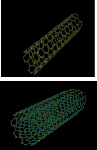
nanotube properties; for example, whether the individual nanotube shell is a metal or semiconductor. Nanotubes are categorized as single-walled nanotubes (SWNTs) and multi-walled nanotubes (MWNTs). Individual nanotubes naturally align themselves into "ropes" held together by vander Waals forces, more specifically, pi-stacking. The single-walled CNT can be either metallic or semiconducting depending on the chirality (i.e., the direction in which the graphene sheet is rolled). The diameter of the CNT is also determined by the chirality [14]. Fig.1 shows single wall CNT and Multi wall CNT. The extraordinary characteristics of carbon Nanotubes make them a promising candidate for applications in microelectronics [15].
Simulation of Carbon nanotubes
The electrical properties of a single wall carbon nanotube offer the potential for molecular-scale electronics, a typical semiconducting single-wall carbon nanotube is 1.4nm in diameter with a 0.6eV band-gap (the band-gap is inversely proportional to the diameter).
Simulation 1
Simulation is performed with carbon nanotube with the following parameters
Figure 2 shows the molecular structure of carbon nanotubes with chirality 9,9 and Figure 3 shows the energy Vs axial vector of CNT for the same input. From the plot we understand the energy levels.
Figure 4 shows the energy with different states of CNTFET and Figure 5 shows the lowest sub band of CNT which intersect at 0 eV level.
Simulation 2
Simulation is performed with carbon nanotube with the following parameters
Figure 1 Single Wall Carbon Nanotube & Multi Wall Carbon Nanotube
structure
Table 1 Simulation parameters 1
S.No. Parameters Value
1. Simulation method Pz orbital
2. Chirality (n,m) 9,9
3. Tight binding 3eV
4. Carbon –carbon spacing 1.42 A
5. Length of the tube 50
Figure 2 Molecular structure of CNT with chirality (9,9)
Figure 3 Energy Vs Axial vector of CNT with chirality (9,9)
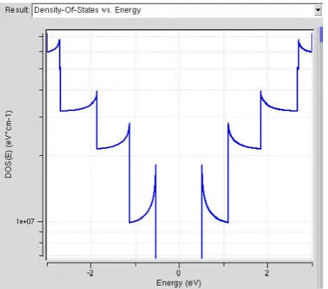
Figure 4 Energy Vs density of states of CNT with chirality (9,9)
Figure 6 shows the molecular structure of carbon nanotubes with chirality 6,0 and Figure 7 shows the energy Vs axial vector of CNT for the same input. From the plot we understand the energy levels.
Figure 8 shows the energy with different states of CNTFET and Figure 5 shows the lowest sub band of CNT which intersect at 0 eV level.
Simulation 3
Simulation is performed with carbon nanotube with the following parameters
Table 2 Simulation parameters
S.No. Parameters Value
1. Simulation method Pz orbital
2. Chirality (n,m) 6,0
3. Tight binding 3eV
4. Carbon –carbon spacing 1.42 A
5. Length of the tube 50
Figure 6 Molecular structure of CNT with chirality (6, 0)
Figure 7 Energy Vs Axial vector of CNT with chirality (6, 0)
Figure 8 Energy Vs density of states of CNT with chirality (6,0)
Figure 9 Lowest sub band of CNT with chirality (6,0)
Table 3 Simulation parameters
S.No. Parameters Value
1. Simulation method Pz orbital
2. Chirality (n,m) 2,9
3. Tight binding 3eV
4. Carbon –carbon spacing 1.42 A
5. Length of the tube 50
Figure 10 Molecular structure of CNT with chirality (2,9)
Figure 10 shows the molecular structure of carbon nanotubes with chirality 2, 9 and Figure 11 shows the energy Vs axial vector of CNT for the same input. From the plot we understand the energy levels.
Figure 11 shows the energy with different states of CNTFET and Figure 12 shows the lowest sub band of CNT which have more depletion gap.
Carbon Nanotubes In Fet & Applications
CNTs can be both metallic and semiconducting depending upon the chirality vector. The promising characteristics of individual Carbon nanotube FETs have guide to early attempts at integration of several CNTFETs into important circuits that can perform an arithmetic and logical operation, or function as memories and sensors. The structure of CNT decides the FET’s operation. The diameter of CNTs gets fixed once a nanotube is grown which fixes the current drive. CNTFET’s width and current drive can be increased by adding nanotubes in parallel. The metal gate through thin gate oxide modulates the electronic band structure of the source, drain and CNT, to regulate the current. Figure.14 (a) Theoretical structure of CNTFET [16]
Main advantages of CNTFETs are threshold voltage control, channel formation, and higher mobility, current density and transconductance gain. The N-type CNTFET produces three times more on-current per unit width at a gate overdrive of 0.6V compared to a p-type MOSFET at the same gate voltage. Limitations include that the CNTs degrade quickly when exposed to ambient air. Therefore, research is underway to coat CNT with polymers in order to increase their lifetime. These type of structures can be used in sensor applications particularly in biomedical where cancer, HIV and other pathogens can be detected at early stages.
CONCLUSION
This concludes our study of CNT properties, simulation with different chirality vector. In this paper we studied the property of carbon nanotubes, types and its modes, we study the carbon nanotube characteristics under the chirality vector of 9,9; 6,0; 2,9. CNT are used in CNT field effect transistor for different sensor applications mainly in biomedical field. CNTFET with different signal conditioning circuit plays an application on biomedical sensor field.
Acknowledgement
The authors would like to acknowledge Nanohub.org for providing permission to access the CNT labs simulation tools and to carry out the experiments.
References
1. Ajayan, Pulickel M., and Otto Z. Zhou. "Applications of carbon nanotubes." Carbon nanotubes. Springer Berlin Heidelberg, 2001. 391-425.
2. Iijima, Sumio, and Toshinari Ichihashi. "Single-shell carbon nanotubes of 1-nm diameter." Nature 363.6430 (1993): 603-605.
3. Endo, Morinobu, Michael S. Strano, and Pulickel M. Ajayan. "Potential applications of carbon nanotubes." Carbon nanotubes. Springer Berlin Heidelberg, 2007. 13-62.
4. Baughman, Ray H., Anvar A. Zakhidov, and Walt A. De Heer. "Carbon nanotubes--the route toward applications." science 297.5582 (2002): 787-792
5. Yakobson, Boris I., and Phaedon Avouris. "Mechanical properties of carbon nanotubes." Carbon nanotubes. Springer Berlin Heidelberg, 2001. 287-327
6. Fan, Shoushan, et al. "Self-oriented regular arrays of carbon nanotubes and their field emission properties." Science 283.5401 (1999): 512-514
7. Ebbesen, T. W., et al. "Electrical conductivity of individual carbon nanotubes." (1996): 54-56.
Figure 12 Energy Vs density of states of CNT with chirality (6,0)
Figure 13 Lowest sub band of CNT with chirality (2,9)
8. Yu, Min-Feng, et al. "Strength and breaking mechanism of multiwalled carbon nanotubes under tensile load." Science 287.5453 (2000): 637-640
9. Ren, Z. F., et al. "Synthesis of large arrays of well-aligned carbon nanotubes on glass." Science 282.5391 (1998): 1105-1107
10. Sun, Ya-Ping, et al. "Functionalized carbon nanotubes: properties and applications." Accounts of Chemical Research 35.12 (2002): 1096-1104
11. Collins, Philip G., et al. "Extreme oxygen sensitivity of
electronic properties of carbon
nanotubes." science 287.5459 (2000): 1801-1804
12. Ruoff, Rodney S., and Donald C. Lorents. "Mechanical and thermal properties of carbon nanotubes." carbon 33.7 (1995): 925-930
13. Geunho Cho, Yong-Bin Kim, and Fabrizio Lombardi, “Modeling Undeposited CNTs for CNTFET Operation”, IEEE Transactions On Device And Materials Reliability, VOL. 11, NO. 2, JUNE 2011,263-272
14. Wang, X.; Li, Qunqing; Xie, Jing; Jin, Zhong; Wang, Jinyong; Li, Yan; Jiang, Kaili; Fan, Shoushan (2009). "Fabrication of Ultralong and Electrically Uniform Single-Walled Carbon Nanotubes on Clean Substrates". Nano
Letters. 9 (9):137141. Bibcode:2009NanoL...9.3137W. d oi:10.1021/nl901260b. PMID 19650638
15. Wolfgang Hoenlein et al., “Carbon Nanotube Applications in Microelectronics”, IEEE
TRANSACTIONS On Components And
PackagingTechnologies , VOL. 27, NO. 4, DECEMBER 2004, 429-434
16. Gupta, Raghav, and Ashwani K. Rana. "Comparative study of digital inverter for CNTFET & CMOS technologies." Engineering (NUiCONE), 2013 Nirma University International Conference on. IEEE, 2013. 17. https://nanohub.org/
*******
How to cite this article: