doi:10.1155/2009/250794
Research Article
Hardware Realization of Generalized Time-Frequency
Distribution with Complex-Lag Argument
Nikola ˇ
Zari´c, Irena Orovi´c, and Srdjan Stankovi´c
Faculty of Electrical Engineering, University of Montenegro, 20000 Podgorica, Montenegro
Correspondence should be addressed to Nikola ˇZari´c,[email protected]
Received 13 July 2009; Accepted 2 December 2009
Recommended by Patrick Oonincx
A hardware implementation of theNth order complex-lag time-frequency distribution is proposed. The considered distribution
provides an arbitrary high concentration for multicomponent signals with fast varying instantaneous frequency. Although the distribution form is quite complex, the proposed realization is very efficient and provides high-speed real-time processing. Further, it allows avoiding miscalculation errors that may appear in the numerical calculation of signal with complex-lag argument. The results of FPGAs (Field Programmable Gate Arrays) implementation are presented as well.
Copyright © 2009 Nikola ˇZari´c et al. This is an open access article distributed under the Creative Commons Attribution License, which permits unrestricted use, distribution, and reproduction in any medium, provided the original work is properly cited.
1. Introduction
Time-frequency analyses have been used in many appli-cations with nonstationary signals, such as speech, radar, seismic, biomedical, and communication signals, and so forth. Various time-frequency distributions have been intro-duced to provide optimal representation in the time-frequency domain. For instance, an ideal representation for linear frequency modulated signals is obtained by using
the quadratic distributions [1–4]. However, they cannot
provide satisfying distribution concentration for signals with higher nonstationarity, since the inner interferences appear. In order to improve concentration, various
higher-order distributions are used: L-Wigner distribution [5],
Polynomial distributions [6,7], as well as the distributions
with complex-lag argument [8–12]. Recently, theNth order
general form of complex-lag time-frequency distribution
for multicomponent signals has been proposed [13]. This
form can provide a cross-terms free representation with an arbitrary high concentration even for signals with significant phase variations within a few samples. Although it produces
very efficient results, MATLAB simulation of theNth order
complex-lag distribution requires significant computational time, inappropriate for real-time processing. Also, the soft-ware simulation has a significant latency and low throughput rate. These drawbacks of the software simulation could be
solved by a suitable hardware realization. Consequently, the favorable properties of the complex-lag distribution could be available in various real-time applications.
A flexible architecture of an arbitrary (Nth) order complex-lag distribution for multicomponent signals is
proposed in this paper. Although it seems that the Nth
order complex-lag distribution is difficult for realization, an
efficient parallel configuration is provided, suitable for VLSI
implementation that allows high-speed real-time processing. The serial realization that reduces number of components is considered as well. The proposed hardware overcomes the errors in the numerical calculations caused by the limited MATLAB software precision, which is an additional advan-tage. Namely, this problem appears in the calculation of analytic extension of the signal with complex-lag argument [9,13].
The proposed system consists of two main parts:
real-ization of the S-method (proposed in [14]) and realization
of the concentration function (system of orderN-2). The
cosine functions) that do not exist as standard components, is given as well.
The paper is organized as follows. The review of generalized time-frequency distribution with complex-lag
argument is given in Section 2. Section 3 presents the
parallel hardware realization of generalized time-frequency
distribution with complex-lag argument, while inSection 4
the serial realization is proposed. Section 5 presents the
analysis and comparison of the proposed system. The FPGA implementation and simulation results are given in
Section 6. Concluding remarks are given in Section 7. The realizations of intermediate calculations are given in the appendix.
2. Theoretical Background
A general discrete form of the Nth order time-frequency
distribution with complex-lag argument can be written as [13]
GCDN(n,k)= Ns/2−1
m=−Ns/2
x(n+m)x(n−m)c(n,m)e−j(2π/Ns)Nmk,
(1)
where (·) denotes complex conjugation,nandkare discrete
time and frequency variables, respectively,Nsis the number
of samples, whilec(n,m) represents the concentration
func-tion:
c(n,m)=
N/2−1
p=1
xwN,p
n+mwN,p N
x−wN,p
n−mwN,p N
,
(2)
where wN,p = ej2π p/N = wrp + jwip. Observe that the
GCDN(n,k) can be expressed as
GCDN(n,k)=N
2WD
n,N
2k
∗kFTm(c(n,m))
=N
2WD
n,N
2k
∗kC(n,k).
(3)
The convolution in frequency domain is denoted by ∗k,
while FTm denotes the Fourier transform with respect to
variable m. The concentration function (of order N-2)
acts as a correction term that can arbitrarily improve the concentration of the Wigner distribution (WD) by increasing
the order N. In order to provide a suitable representation
for multicomponent signals, the Nth order complex-lag
distribution has been modified [13]. The modifications are
introduced in the calculation of the concentration function
(for the qth signal component): c(n,m)q = cr(n,m)q ·
ci(n,m)q, where
cr(n,m)q= N/2−1
p=1
crp(n,m)q
=
N/2−1
p=1
ejwrpangle(xap(n+m(wN,p/N))q·xap(n−m(wN,p/N))q),
ci(n,m)q= N/2−1
p=1
cip(n,m)q
=
N/2−1
p=1
e−jwipln|xap(n+m(wN,p/N))q·xap(n−m(wN,p/N))q|.
(4)
More details could be found in [13]. Calculation of
signal with complex-lag argument xap(n±m(wN,p/N))q is
considered later in this section.
The time-frequency representations of the resulting functionscr(n,m) andci(n,m) (for all signal components) are obtained as
Cr(n,k)=FTm
⎧ ⎨ ⎩
Q
q=1
cr(n,m)q
⎫ ⎬ ⎭,
Ci(n,k)=FTm
⎧ ⎨ ⎩
Q
q=1
ci(n,m)q
⎫ ⎬ ⎭,
(5)
whereQis the number of signal components.
The final form of the concentration function in the time-frequency domain is the convolution ofCr(n,k) andCi(n,k):
C(n,k)=
Ld
i=−Ld
P(i)Cr(n,k+i)Ci(n,k−i). (6)
Note thatP(i) is a frequency domain window of the size
2Ld+ 1. The cross-terms free representation is obtained if the
size of window is less than the minimal distance between the autoterms.
Finally, a general form of modified complex-lag time-frequency distribution is defined as
MGCDN(n,k)=
Ld
i=−Ld
P(i)SM(n,k+i)C(n,k−i), (7)
where, instead of the WD, the S-method (cross-terms free
WD), SM(n,k)=Ld
i=−LdP(i)STFT(n,k+i)STFT(n,k−i), is
used. The acronym STFT is used for the short time Fourier transform.
[9]. Then theqth component of the signal with complex-lag argument is calculated by using the analytic extension as follows [13]:
xap
n±mwN,p N
q=
kq+Wq
k=kq−Wq
STFTn,k+kq(n)
×ej2π(n±m(wN,p/N))k/Ns.
(8)
It is assumed that theqth signal component is within
the region [kq(n) − Wq,kq(n) + Wq] where kq(n) =
arg{maxkSTFT(n,k)}is the position of its maximum. The
parameterWqis used to define the width (2Wq+ 1) of the
q-th signal component in q-the time-frequency plane. The
cross-terms will be avoided if 2Wq+ 1 is smaller than the distance
between autoterms. The width 2Wq+ 1 could be adjusted for
each signal component [14].
Note that the real part of exponential function
exp(jmkwN,p/N), for large values of mk, can exceed the
computer (software) precision range, and it may cause errors in the numerical realization.
3. Parallel Architecture for
Implementation of the
N
th Order
Complex-Lag Time-Frequency Distribution
A system for implementation of the Nth order
complex-lag time-frequency distribution for multicomponent signals is proposed in this section. The block scheme is given in
Figure 1. The starting block is the calculation of the STFT that is used to obtain the S-method (SM(n,k)). According to
(8), the STFT is also used to obtain the signal with
complex-lag argument for the computation ofC(n,k) (by using (4),
(5), and (6)). The S-method is obtained at the output of
the SM block, while the C(n,k) is obtained at the output
of the BLOCK 4 in Figure 1. The complex-lag distribution
(MGCD(n,k)) is produced at the output of the BLOCK 5, as
a convolution of the SM(n,k) andC(n,k).
3.1. Hardware Solutions for the STFT and the SM. The
architectures for the STFT and the SM implementation have
been proposed in [14]. They are shown in Figures2(a)and
2(b), respectively. Namely, by using the rectangular window,
the STFT is realized as [15,16]
STFTRe(n,k)=(−1)k
x
n+Ns
2
−x
n−Ns 2
+c(k)STFTRe(n−1,k)
−s(k)STFTIm(n−1,k),
STFTIm(n,k)=c(k)STFTIm(n−1,k)
+s(k)STFTRe(n−1,k),
(9)
where, for a givenk, the quantitiesc(k)=cos(2πk/Ns) and
s(k)=sin(2πk/Ns) are constants. The STFT(n,k) represents
the input for the SM realization. Thus, the SM is obtained
according to the form presented in [14]:
SM(n,k)= |STFT(n,k)|2
+ 2 Ld
i=1
STFTRe(n,k+i)STFTRe(n,k−i)
+ 2 Ld
i=1
STFTIm(n,k+i)STFTIm(n,k−i).
(10)
3.2. Hardware Solution for the Concentration Function in Time-Frequency Domain C(n,k). The parallel architecture for concentration function in the time-frequency domain
is realized through several blocks in Figure 1: STFT block,
BLOCK 1, BLOCK 2, BLOCK 3, and BLOCK 4. The outputs of the STFT block used in the calculation of the concen-tration function are STFTc(n,k) = (N/2)STFT(n, (N/2)k). The separation of signal components is performed within
the BLOCK 1, while the BLOCK 2 is used for cr(n,m)
and ci(n,m) calculation. The Fourier transforms of these
functions (Cr(n,k) andCi(n,k)) are performed in BLOCK 3.
The final form of the concentration functionC(n,k) (in the
time-frequency domain) is obtained at the output of BLOCK 4.
In the sequel, each block will be analyzed and presented separately.
3.2.1. BLOCK 1: Separation of Signal Components. The
regions that contain signal components are separated within BLOCK 1, based on the outputs of the STFT block. In this sense, it is necessary first to allocate components of
|STFTc(n,k)| that are higher than the reference value R.
For instance, if the signal amplitudes are normalized, the
STFT values are in the range [−1, 1], and the reference value
should be set toR =1/λ, whereλis a scaling constant and
λ ≥ 1 holds. Otherwise, if the signal range is unknown,
the reference value is defined as a portion of the STFT’s
maximum at a given instant n, R = maxk|STFTc(n,k)|/λ.
The regions of STFTc(n,k) that are higher than Rcontain
the signal components. Each of them is further processed to
find the position of its maximal component denoted bykq,
q = 1,. . .,Q, whereQis the number of allocated regions, that is, the number of signal components. The outputs STFTc(n,k) fork ∈ [kq −Wq,kq+Wq] are passed to the inputs of BLOCK 2.
3.2.2. BLOCK 2: Realization of the Concentration Func-tions cr(n,m)and ci(n,m). Hardware solutions for xap(n+
wN,pm/N)qandxap(n−wN,pm/N)q represent an initial step in the realization of BLOCK 2. They are shown in Figures
3(a) and 3(b), respectively. For the pth term in (4) and
the qth signal component, the two channels (real and
cr(p=1)(n,m))
ci(p=1)(n,m))
cr(p=2)(n,m))
ci(p=2)(n,m))
cr(p=N/2−1)(n,m))
ci(p=N/2−1)(n,m)) Forq=1 Form=1
Form=Ns
k=0
STFT(n,k)
k=Ns
k1−Wq
k1+Wq
kq−Wq
kq+Wq
kQ−Wq
kQ+Wq
Forq=Q
Form=1 Form=Ns
Form=1
Form=Ns
cr(n,m)q
ci(n,m)q
cr(n,m)1
cr(n,m)Q
ci(n,m)1
ci(n,m)Q
cr(n,m)
ci(n,m)
Cr(n, 1)
Cr(n,Ns)
Ci(n, 1)
Ci(n,Ns)
C(n, 1)
C(n,Ns)
SM(n, 1)
SM(n,Ns)
Signal
STFT .
.
. X
X +
+
m=1 FFT
m=Ns
m=1 FFT
m=Ns . . .
. . .
Conv
SM . . .
. . .
Conv
MGCD(n, 1)
MGCD(n,Ns) BLOCK1
BLOCK2
BLOCK3 BLOCK4
BLOCK5
k=0
k=Ns
Figure1: Parallel architecture for realization of generalized complex-lag distribution for multicomponent signals.
A/D
Clock
R1
R2
RN
Mult Mult Mult Mult
VCC
VCC
VCC
Cin
Cin
. . .
. . .
. .
. STFTRe(n−1,k)
STFTIm(n−1,k)
k=0
k=1
clk
clk +
+
+
+
S(k)
C(k)
(a)
SM(n,k) STFTRe(n,k−Ld)
STFTRe(n,k+Ld) STFTRe(n,k−Ld+ 1) STFTRe(n,k+Ld−1)
STFTRe(n,k−1)
STFTRe(n,k+ 1)
STFTRe(n,k)
STFTIm(n,k)
STFTIm(n,k+ 1)
STFTIm(n,k−1)
STFTIm(n,k+Ld−1) STFTIm(n,k−Ld+ 1) STFTIm(n,k+Ld) STFTIm(n,k−Ld)
Mult Mult
Mult Mult Mult Mult
Mult Mult
SH SH
SH
SH
SH SH
+ +
+ +
+
+ +
+ + .
. .
. . .
(b)
STFTcRe(n,kq−Wq)
STFTcIm(n,kq−Wq)
STFTcRe(n,kq−1)
STFTcIm(n,kq−1)
STFTcRe(n,kq)
STFTcIm(n,kq)
STFTcRe(n,kq+ 1)
STFTcIm(n,kq+ 1)
STFTcRe(n,kq+Wq)
STFTcIm(n,kq+Wq)
Re(xap(n+wN,pm/N)q)
Im(xap(n+wN,pm/N)q)
Mult Mult Mult Mult Mult Mult Mult Mult Mult Mult Mult Mult Mult Mult Mult Mult Mult Mult Mult Mult
+
+
+
+
+
+
+
+
+
+ +
+
+
+ +
+
+
+ +
+ +
+
Cin
Cin
Cin
Cin
Cin
. . .
. . .
. . . . . .
. . .
. . .
A(m,k)
B(m,k)
A(m,k)
B(m,k)
A(m,k)
B(m,k)
A(m,k)
B(m,k)
A(m,k)
B(m,k)
VCC
VCC
VCC
VCC
VCC
(a)
STFTcRe(n,kq−Wq)
STFTcIm(n,kq−Wq)
STFTcRe(n,kq−1)
STFTcIm(n,kq−1)
STFTcRe(n,kq)
STFTcIm(n,kq)
STFTcRe(n,kq+ 1)
STFTcIm(n,kq+ 1) STFTcRe(n,kq+Wq)
STFTcIm(n,kq+Wq)
Re(xap(n−wN,pm/N)q)
Im(xap(n−wN,pm/N)q)
Mult Mult Mult Mult Mult Mult Mult Mult Mult Mult Mult Mult Mult Mult Mult Mult Mult Mult Mult Mult
+
+
+
+
+
+
+
+
+
+ +
+
+
+ +
+
+
+ +
+ +
+
Cin
Cin
Cin
Cin
Cin
. . .
. . .
. . . . . .
. . .
. . .
A1(m,k)
B1(m,k)
A1(m,k)
B1(m,k)
A1(m,k)
B1(m,k)
A1(m,k)
B1(m,k)
A1(m,k)
B1(m,k)
VCC
VCC
VCC
VCC
VCC
(b)
xap(n+wN,pm/N)q (Figure 3(a)) are obtained according to (8):
Re
xap
n+wN,pm/N
q
=
k+Wq
k=kq−Wq
(A(m,k)STFTcRe(n,k)−B(m,k)STFTcIm(n,k)),
Im
xap
n+wN,pm/N
q
=
kq+Wq
k=kq−Wq
(A(m,k)STFTcIm(n,k) +B(m,k)STFTcRe(n,k)).
(11)
The constantsA(m,k) andB(m,k) are defined as
A(m,k)=(−1)kcoswrp2πkm
Ns e
−wip2πkm/Ns,
B(m,k)=(−1)ksinwrp2πkm
Ns e
−wip2πkm/Ns.
(12)
Similarly, real and imaginary parts ofxap(n−wN,pm/N)q (Figure 3(b)) are obtained by using the constants:
A1(m,k)=(−1)kcos
wrp2πkm
Ns e
wip2πkm/Ns,
B1(m,k)=(−1)k+1sin
wrp2πkm
Ns e
wip2πkm/Ns,
(13)
instead ofA(m,k) andB(m,k).
Note that the hardware components should provide satisfying precision even for large values of real exponential
term exp(wip2πmk/Ns) (for large m and k). The required
precision depends on the number of input samplesNsand
the distribution orderNsince−Ns/2 ≤m≤ Ns/2−1 and
−Ns/N ≤ k ≤ Ns/N hold. Thus, the miscalculation errors
will be avoided if registers are designed to store the value log2(e2πNs/2). For example, if N
s = 128 and N = 4, the
extended single precision IEEE-754 format should be used,
while forNs=256, the extended double precision IEEE-754
format is required.
In the sequel, xap(n±wN,pm/N)q is used to calculate
the concentration functions crp(n,m)q and cip(n,m)q (for the pth term in (4) and the qth signal component). The
architecture forcrp(n,m)qandcip(n,m)qis given inFigure 4. The realization is done according to
Recrp(n,m)q
=Reejwrpangle((a+jb)/(c+jd))
=cos
wrp·atan
bc−ad ac+bd
,
Imcrp(n,m)q
=Imejwrpangle((a+jb)/(c+jd))
=sin
wrp·atan
bc−ad ac+bd
,
Recip(n,m)q
=Reejwipln|(c+jd)/(a+jb)|
=cos
1 2wip
lnc2+d2−lna2+b2,
Imcip(n,m)q
=Imejwipln|(c+jd)/(a+jb)|
=sin
1 2wip
lnc2+d2−lna2+b2,
(14)
where, to simplify the expressions, the following notations are used:
a=Re
xap
n+wN,pm/N
q
,
b=Im
xap
n+wN,pm/N
q
,
c=Re
xap
n−wN,pm/N
q
,
d=Im
xap
n−wN,pm/N
q
.
(15)
The outputs of architecture inFigure 4(defined by (14)),
are further combined for allp:p=1,. . .,N/2−1, as
cr(n,m)q= N/2−1
p=1
Recrp(n,m)q
+jImcrp(n,m)q
,
ci(n,m)q= N/2−1
p=1
Recip(n,m)q
+jImcip(n,m)q
.
(16)
The realizations ofcr(n,m)q andci(n,m)q are shown in
Figures5(a)and5(b), respectively.
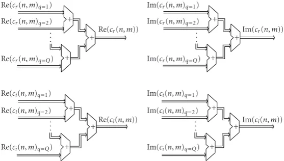
By taking all signal components, the resulting concentra-tion funcconcentra-tionscr(n,m) andci(n,m) (Figure 6) are obtained:
Re{cr(n,m)} = Q
q=1
Recr(n,m)q
,
Im{cr(n,m)} = Q
q=1
Imcr(n,m)q
a=Re(xap(n+wN,pm/N)q)
b=Im(xap(n+wN,pm/N)q) c=Re(xap(n−wN,pm/N)q)
d=Im(xap(n−wN,pm/N)q)
Mult Mult Mult Mult Mult Mult Mult Mult
Mult
Mult +
+
+
+
+
VCC
VCC
Cin
Cin
ln
ln Div
cos
cos sin
sin atan
wr,p
1/2wi,p
Re(crp(n,m)q)
Im(crp(n,m)q)
Re(cip(n,m)q) Im(cip(n,m)q)
Figure4: Architecture for realization of concentration functionscrp(n,m)qandcip(n,m)q.
Re(cr(p=1)(n,m)q) Im(cr(p=1)(n,m)q)
Re(cr(p=2)(n,m)q) Im(cr(p=2)(n,m)q)
Re(cr(p=N/2−1)(n,m)q) Im(cr(p=N/2−1)(n,m)q)
Re(cr(n,m)q)
Im(cr(n,m)q) Mult
Mult Mult Mult
Mult Mult Mult Mult
Mult
Mult
Mult
Mult +
+
+
+
+
+
VCC
VCC
VCC
Cin
Cin
Cin
. . . . . .
(a)
Re(ci(p=1)(n,m)q) Im(ci(p=1)(n,m)q)
Re(ci(p=2)(n,m)q) Im(ci(p=2)(n,m)q)
Re(ci(p=N/2−1)(n,m)q) Im(ci(p=N/2−1)(n,m)q)
Re(ci(n,m)q)
Im(ci(n,m)q) Mult
Mult Mult Mult
Mult Mult Mult Mult
Mult
Mult
Mult
Mult +
+
+
+
+
+
VCC
VCC
VCC
Cin
Cin
Cin
. . . . . .
(b)
Re(cr(n,m)q=1)
Re(cr(n,m)q=2)
Re(cr(n,m)q=Q)
Re(ci(n,m)q=1)
Re(ci(n,m)q=2)
Re(ci(n,m)q=Q)
Re(cr(n,m))
Re(ci(n,m))
Im(cr(n,m)q=1)
Im(cr(n,m)q=2)
Im(cr(n,m)q=Q)
Im(ci(n,m)q=1)
Im(ci(n,m)q=2)
Im(ci(n,m)q=Q)
Im(cr(n,m))
Im(ci(n,m)) +
+
+
+ +
+
+
+
+
+ +
+ .
. .
. . .
. . .
. . .
Figure6: Architecture for resulting concentration functionscr(n,m) andci(n,m).
Re{ci(n,m)} = Q
q=1
Reci(n,m)q
,
Im{ci(n,m)} = Q
q=1
Imci(n,m)q
.
(17)
3.2.3. BLOCK 3: Realization of Functions Cr(n,k) and
Ci(n,k). The architecture inFigure 7is used to obtain
time-frequency domain functions:Cr(n,k)=FFT{cr(n,m)}, and
Ci(n,k) = FFT{ci(n,m)} (FFT denotes the fast Fourier
transform). Since the real and imaginary parts are treated
separately, the outputs of FFT circuits in Figure 7 are
obtained in the form:
F1(n,k)=Re{FFT(Re{cr(n,m)})},
F2(n,k)=Im{FFT(Re{cr(n,m)})},
F3(n,k)=Re{FFT(Im{cr(n,m)})},
F4(n,k)=Im{FFT(Im{cr(n,m)})},
F5(n,k)=Re{FFT(Re{ci(n,m)})},
F6(n,k)=Im{FFT(Re{ci(n,m)})},
F7(n,k)=Re{FFT(Im{ci(n,m)})},
F8(n,k)=Im{FFT(Im{ci(n,m)})}.
(18)
Therefore, the real and imaginary parts of functions Cr(n,k) and Ci(n,k) (the outputs of adders in Figure 7) follow as
Re{Cr(n,k)} =F1(n,k) +F3(n,k),
Im{Cr(n,k)} =F2(n,k) +F4(n,k),
Re{Ci(n,k)} =F5(n,k) +F7(n,k),
Im{Ci(n,k)} =F6(n,k) +F8(n,k).
(19)
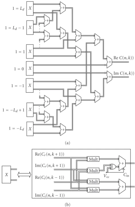
3.2.4. BLOCK 4: The Final Form of the Concentration Function in the Time-Frequency Domain. The concentration function C(n,k) is obtained as a convolution of functionsCr(n,k) and
Ci(n,k):
Re{C(n,k)} =
Ld
l=−Ld
Re{Cr(n,k+l)Ci(n,k−l)},
Im{C(n,k)} =
Ld
l=−Ld
Im{Cr(n,k+l)Ci(n,k−l)}. (20)
The architecture is shown inFigure 8(a) Note that, the
realization of the product termCr(n,k+l)Ci(n,k−l), shown inFigure 8(b), is done according to
Re{Cr(n,k+l)Ci(n,k−l)}
=Re{Cr(n,k+l)}Re{Ci(n,k−l)}
−Im{Cr(n,k+l)}Im{Ci(n,k−l)},
Im{Cr(n,k+l)Ci(n,k−l)}
=Re{Cr(n,k+l)}Im{Ci(n,k−l)}
+ Im{Cr(n,k+l)}Re{Ci(n,k−l)}.
(21)
In the final step, a convolution of SM(n,k) andC(n,k) is
performed within BLOCK 5 (Figure 1) and the channels of
theNth order complex-lag time-frequency distribution are obtained as
Re{MGCD(n,k)} =
Ld
i=−Ld
Re{SM(n,k+i)C(n,k−i)},
Im{MGCD(n,k)} =
Ld
i=−Ld
Im{SM(n,k+i)C(n,k−i)}.
(22)
The corresponding architecture is given inFigure 9. Note
that the convolution of SM(n,k) andC(n,k) is realized in the
same way as the convolution of STFT(n,k) and STFT(n,k)
Re(cr(n,m))
Im(cr(n,m))
Re(ci(n,m))
Im(ci(n,m))
Re(Cr(n,k))
Im(Cr(n,k))
Re(Ci(n,k))
Im(Ci(n,k))
k=1
FFT
k=Ns
k=1
FFT
k=Ns
k=1
FFT
k=Ns
k=1
FFT
k=Ns
F1(n,k)
F2(n,k)
F3(n,k)
F4(n,k)
F5(n,k)
F6(n,k)
F7(n,k)
F8(n,k)
+
+
+
+ .
. . . . .
. . . . . .
. . . . . .
. . .
. . .
. . .
. . .
. . .
. . .
. . .
. . .
. . .
. . .
Figure 7: Architecture for realization of Cr(n,k) and Ci(n,k)
functions.
4. Serial Architecture for
Implementation of the
N
th Order
Complex-Lag Time-Frequency Distribution
As an alternative to the proposed system with parallel
realization, a serial architecture for implementation of the
N-th order complex-lag distribution is considered. The block
scheme for serial architecture is given inFigure 10.
The STFT block is the same as in the parallel realization, while the serial architecture for the S-method (SM block)
is given in [14]. The concentration function is obtained
throughout the following blocks (Figure 10): BLOCK1,
BLOCK2, BLOCK3, and BLOCK4. BLOCK1 (the separation of signal components) and BLOCK3 (the FFT calculation) are the same as in the parallel realization. Therefore, the main modifications with respect to the parallel realization are made within BLOCK2. It consists of Block21, Block22, Block23, and Block24, that will be briefly discussed in the sequel.
Block21. This block is used for the calculation of signal
with complex-lag argument, given by (11). The realization
is shown inFigure 11. The LUT (Look-Up Table) contains
the constants: A(m,k), B(m,k), A1(m,k), and B1(m,k),
defined by (12) and (13), respectively. Address 1 and
Address 3 are used to provide synchronization between
1=Ld
1=Ld−1
1=1
1=0
1= −1
1= −Ld+ 1
1= −Ld
ReC(n,k))
ImC(n,k))
X
X
X
X
X
X
X
. . . . . .
. . . . . .
+ +
+ +
+
+
+
+ +
+
+ +
+
+ + +
(a)
X
Re(Cr(n,k+ 1)) Im(Cr(n,k+ 1)) Re(Ci(n,k−1))
Im(Ci(n,k−1))
+
+ Mult
Mult Mult Mult
Vcc Cin
(b)
Figure 8: Architecture for realization of (a) C(n,k) and (b) realization of productCr(n,k+l)Ci(n,k−l) for certainl.
the STFT samples and the LUT elements. One summation
term in (11) is obtained within one cycle of the clk6
clock, while the complete summation is performed within
one cycle of clk1. The terms Re{xap(n+wN,pm/N)q},
Im{xap(n+wN,pm/N)q}, Re{xap(n−wN,pm/N)q}, and Im{xap(n−wN,pm/N)q}are obtained within the four cycles of clk1. After each cycle of clk1, the RESET1 signal resets the cumulative adder ADD.
Block22. The outputs of Block21 are fed to the input of Block22 that is used to obtain concentration functions crp(n,m)qandcip(n,m)q.The serial realization of these
func-tions is the same as in the parallel architecture (Figure 4).
Block23. It calculates the resulting concentration func-tionscr(n,m)qandci(n,m)qdefined by (16). The realization
is given inFigure 12. The Address 4 and Address 5 determine
Re(C(n,k+Ld)) Im(C(n,k+Ld)) SM(n,k−Ld)
Re(C(n,k+Ld−1)) Im(C(n,k+Ld−1)) SM(n,k−Ld+ 1)
Re(C(n,k+ 1)) Im(C(n,k+ 1)) SM(n,k−1) Re(C(n,k)) Im(C(n,k)) SM(n,k) Re(C(n,k−1)) Im(C(n,k−1)) SM(n,k+ 1)
Re(C(n,k−Ld+ 1)) Im(C(n,k−Ld+ 1)) SM(n,k+Ld−1)
Re(C(n,k−Ld)) Im(C(n,k−Ld)) SM(n,k+Ld)
Mult Mult Mult Mult
Mult Mult Mult Mult Mult Mult
Mult Mult Mult Mult
+
+
+
+
+
+
+
+ +
+
+
+
+
+ +
+ .
. . . . .
. . .
. . .
Re(MGCD(n,k))
Im(MGCD(n,k))
Figure9: Architecture for realization of convolution between SM(n,k) andC(n,k).
k=0
STFT(n,k)
k=K
k1−Wq
k1+Wq
kq−Wq
kq+Wq
kQ−Wq
kQ+Wq
Address 1 clk1 clk2 clk3 clk4 clk5
Address2 SM(n, 1)
SM(n,k)
cr(n,m)
ci(n,m)
m=1 FFT
m=M
m=1 FFT
m=M Cr(n, 1)
Cr(n,k)
Ci(n, 1)
Ci(n,k)
C(n, 1)
C(n,k) Signal
STFT
Form=1
Mu
x
Mu
x
+ ...
. . .
. . .
. . . Conv1
SM
Conv2
MGCD(n, 1)
MGCD(n,K) BLOCK1
BLOCK2
Block21 Block22 Block23
Block24 BLOCK3 BLOCK4
BLOCK5
k=0
k=K
Figure10: Serial architecture for realization of generalized complex-lag distribution for multicomponent signals.
Im{ci(n,m)q}are obtained after 4(N/2-1) cycles. The
cumu-lative multiplier Mult1 should be reset after eachN/2-1 cycles
of clk8.
Block24. The final concentration functionscr(n,m) and
ci(n,m) are obtained at the output of this block. One cycle
of the clk4 is set to the time interval that is necessary for the calculations within the three previous blocks. Address 2
determines the order of inputs in BLOCK3,Figure 10. The
concentration functionsCr(n,k) andCi(n,k) are obtained at the output of BLOCK3.
BLOCK4 is used to perform the calculation of
concen-tration functionC(n,k) defined by (20). The realization of
this block is given in Figure 13. One term in summation
is calculated within one cycle of the clk9, while complete
sum is obtained after 2Ld + 1 cycle. The clock cycles and
reset signals of this circuit are similar as in Block23. The resulting complex-lag distribution is obtained at the output
of BLOCK5 in Figure 10. The realization of this block is
similar to the realization of BLOCK4. The only difference is
STFTcRe(n,kq−Wq) STFTcRe(n,kq−Wq) STFTcRe(n,kq) STFTcIm(n,kq) STFTcRe(n,kq+Wq) STFTcIm(n,kq+Wq)
Address1 Address3 clk6 Reset1 clk1
. . . . . .
Mux
LUT
Mult + ADD
Re{xap(n+wN,pm/N)q}
Im{xap(n+wN,pm/N)q} Re{xap(n−wN,pm/N)q}
Im{xap(n−wN,pm/N)q}
Figure11: Serial architecture for producing of signal with complex-lag argument (Block21).
Re{cr(p=1)(n,m)q} Im{cr(p=1)(n,m)q} Re{ci(p=N/2−1)(n,m)q} Im{ci(p=N/2−1)(n,m)q}
Address3 Address4 clk7 Reset2
clk8 Reset3
clk3 . . .
Mux
Mux Mult
+ ADD
Mult1
Re{cr(n,m)q} Im{cr(n,m)q} Re{ci(n,m)q} Im{ci(n,m)q}
Figure 12: Serial Architecture for realization of concentration functionscr(n,m)qandci(n,m)q(Block23).
Re{Cr(n,k+Ld)} Im{Cr(n,k+Ld)} Re{Ci(n,k−Ld)} Im{Ci(n,k−Ld)}
Address5 Address6 clk9 Reset4
clk10 Reset5
clk11 . . .
+ + Mux
Mux Mult
ADD1
ADD2 Re(C(n,k)) Im(C(n,k))
Figure13: Serial architecture for realization ofC(n,k) (BLOCK 4).
5. Analysis of the Proposed System
In the sequel, some practical issues related to the realization of the proposed hardware realizations are addressed. The proposed system (either with parallel or serial architecture) can be implemented by using the hardware components with floating point format to provide satisfying precision for the calculation of signal with complex-lag argument. However, the floating point adders and multipliers introduce the output latency of few clock cycles. Thus, in order to decrease the output latency, the number of hardware components with floating point format should be reduced. The large values that require high precision appear only
in the realization of concentration functionscrp(n,m)q and
cip(n,m)q (Figures3and4in parallel realization,Figure 11
Table1: Number of circuits for parallel realization.
Adders Multipliers Other circuits
Figure 2 2(Ld+ 2) 2(Ld+ 3)
Figure 3 8Wq+ 2 8Wq+ 4
Figure 4 5(N/2−1) 10(N/2−1) 2ln, divide, atan, cos, sin
Figure 5 N−4 4(N/2−2)
Figure 6 4(Q−1)
Figure 7 4(2 + log2Ns) 4 log2Ns
Figure 8 8Ld+ 2 8Ld+ 4
Figure 9 4Ld 2Ld+ 2
in serial realization). The remaining part of the system can be realized by using the fixed point format. Note that starting
from the output of the system shown inFigure 4(the outputs
of cos and sin circuits), all values will be in the range
[−1, 1], and the fixed point notation could be used. Also, by
normalization of input signal, the STFT and the SM can be calculated by using the fixed point format.
The floating point multipliers increment the exponent by 1, which should be corrected at the output. The fixed point multipliers result in a two sign-bit. Thus, to correct the result, the product has to be shifted left by one bit. This shifter can be included as a part of multiplier.
The total number of circuits needed for one channel of the proposed system for parallel realization is given in
Table 1. The longest path is given in Table 2. It connects
the register storing STFT(n−1,k ±Wq) with the output
MGCD(n,k). The length of this path determines the fastest
sampling rate.
The number of required circuits and longest path for
serial realization are given in Tables3and4, respectively.
In order to compare the parallel and serial realizations the
following values are considered:Ns=128,N =6,Wq =2,
Ld = 2, andQ= 2. The number of hardware components
and the latency for parallel and serial realizations are given in
Table 5.
Table2: The longest path of parallel realization.
Adders Multipliers Other circuits
Figure 2 Ld+ 3 2
Figure 3 2Wq 1
Figure 4 1 2 (cos or sin) and
((div+atan) or (ln+add)) Figure 5log2(N/2−1) log2(N/2−1)
Figure 6 log2Q
Figure 7 1 + log2Ns log2Ns
Figure 8 Ld+ 2 1
Figure 9 Ld+ 1 1
Table3: Number of circuits for serial realization.
Adders Multipliers Other circuits
STFT 4 4
SM 1 1 Mux
Block21 1 1 Mux, LUT
Block22 5 10 2ln, divide, atan, cos, sin
Block23 1 2 2 Mux
Block24 1 Mux
BLOCK3 4(2 + log2Ns) 4 log2Ns
BLOCK4 4 4 Mux
BLOCK5 2 2 Mux
Table4: The longest path of serial realization.
Adders Multipliers Other circuits
STFT 2 1
SM 2Ld+1 Ld+1
Block21 4(2Wq+1) 4(2Wq+1)
Block22 N/2-1 2(N/2-1) ((cos or sin) and
((div+atan) or (ln+add)))
Block23 (N/2-1) 2(N/2-1)
Block24 Q Q
BLOCK3 log2Ns log2Ns
BLOCK4 2(2Ld+1) 2Ld+1
BLOCK5 2Ld+1 2Ld+1
Table5: Comparison between parallel and serial realization.
Parallel realization Serial realization
Adders Multipliers Adders Multipliers
No. of circuits 190 216 55 52
Latency 25 15 189 341
speed, we will consider parallel realization for the FPGA implementation.
6. FPGA Implementation of
the Proposed Parallel Architecture
The proposed architecture can be implemented by using various hardware devices. As one of the possible choices,
C function chip
FFT chip
Conv chip SM
chip
MGCD(n,k)
Figure14: A block scheme for the FPGA implementation.
Table6: Characteristics for the chip inFigure 16.
EP3C40F780C6No. of Logic Speed Power
pins elements consumption
Available 535 39600 500 MHz 1.2 V
Utilized 474 (88%) 8284 (21%) 91 MHz 1.2 V
Table7: Characteristics for the chip inFigure 17.
EP3C16F484C6No. of Logic Speed Power
pins elements consumption
Available 347 15408 500 MHz 1.2 V
Utilized 220 (63%) 6836 (44%) 158 MHz 1.2 V
the digital signal processor could be used. However, it is not suitable for real-time processing, especially at very high speeds. Therefore, for high-speed processing, one might consider the ASIC implementation (application specific integrated circuit) or the FPGA implementation. Both of them allow a high degree of parallelism, as well. ASIC implementation can provide lower power consumption, design size optimization, and design flexibility that enables speed optimization. However, long production time and significant costs do not recommend ASIC device for pro-totype development. The main advantages of the FPGA implementation are reconfigurability, lower producing time and costs requirements, inbuilt special hardware such as RAM, and so forth. Thus, we use the FPGA to develop the prototype that, after testing and verifying the results, can be
implemented on an ASIC. The FPGA chips from Altera [17]
and the Quartus II v8.0 software are used in the proposed implementation.
The fourth-order (N = 4) complex-lag distribution is
considered for FPGA implementation. A simplified block
scheme of the system is shown in Figure 14. The FPGA
implementation of the S-method (SM Chip), including the
chip parameters and performance, has been provided in [14].
Thus, we focus on designing the chip for the concentration
functionc(n,m) (C function Chip). The output of this chip
is passed to the input of the FFT Chip (that produceC(n,k)).
Note that a solution for the FFT chip by using the FFT MegaCore function has recently been proposed by Altera
[18]. For device EP3SE50F780C2 (Stratix III family) and
the 16-bit fixed point format, this FFT chip requires 4290
STFTRe(n,k)
STFTRe(n,k−4)
STFTRe(n,k−2)
STFTRe(n,k+ 4)
STFTRe(n,k+ 2)
STFTIm(n,k)
STFTIm(n,k−4)
STFTIm(n,k−2)
STFTIm(n,k+ 4)
STFTIm(n,k+ 2)
STFTRe(n,k)
STFTRe(n,k−4)
STFTRe(n,k−2)
STFTRe(n,k+ 4)
STFTRe(n,k+ 2)
STFTIm(n,k)
STFTIm(n,k−4)
STFTIm(n,k−2)
STFTIm(n,k+ 4)
STFTIm(n,k+ 2)
Mult Mult Mult Mult Mult
Mult Mult Mult Mult Mult
Mult Mult Mult Mult Mult
Mult Mult Mult Mult Mult
Mult
Mult
Mult
Mult
Block1 Block2
Re(ci(n,m))
Im(ci(n,m)) Re(xap(n+jm))=a
Im(xap(n+jm))=b
Re(xap(n+jm))=c
Im(xap(n+jm))=d
VCC Cin
ln
ln
cos
sin +
+
+
+
+
+
+
+ +
+
+
+ +
+
+
+
+
+
+
A(m,k)
A(m,k−4)
A(m,k−2)
A(m,k+ 4)
A(m,k+ 2)
A(m,k)
A(m,k−4)
A(m,k−2)
A(m,k+ 4)
A(m,k+ 2)
A1(m,k)
A1(m,k−4)
A1(m,k−2)
A1(m,k+ 4)
A1(m,k+ 2)
A1(m,k)
A1(m,k−4)
A1(m,k−2)
A1(m,k+ 4)
A1(m,k+ 2)
Figure15: Architecture for concentration function calculation.
transform time 0.37 microseconds. The outputs from the SM chip and the FFT chip are convolved in the final step, where the convolution circuit (Conv Chip) is realized in the same way as the SM chip.
Realization of the C function Chip.In the case N = 4,
wN,p=wr+jwi= jholds. Consequently, the concentration
function is obtained asc(n,m)=ci(n,m), sincecr(n,m)= 1. The calculation of signal with complex-lag argument is
reduced with respect to (11), since B(m) = 0, and the
corresponding architecture is shown inFigure 15(the Block
1). The remaining components for the realization are given
in Block 2, Figure 15. The schematic diagram for FPGA
realization of signal Re{xap(n+jm)} =a is given inFigure 16.
In order to avoid miscalculations of the analytic extension, the extended single precision floating point arithmetic is
VCC clock_mult Input
Clock cycles: 7 Single extended precision Exponent width: 11 Mantissa width: 31 Direction: add
dataa[42..0] datab[42..0]
clock
result[42..0]
overflow
nan
zero
altfp_add_sub0
inst1
Clock cycles: 7 Single extended precision Exponent width: 11 Mantissa width: 31 Direction: add
dataa[42..0] datab[42..0]
clock
result[42..0]
overflow
nan
zero
altfp_add_sub0
inst3
Clock cycles: 7 Single extended precision Exponent width: 11 Mantissa width: 31 Direction: add
dataa[42..0] datab[42..0]
clock
result[42..0]
overflow
nan
zero
altfp_add_sub0
inst5
Clock cycles: 5 Input/output bus width: 43
dataa[42..0] datab[42..0]
clock
result[42..0]
overflow
nan
zero
altfp_mult0
inst15
Clock cycles: 5 Input/output bus width: 43
dataa[42..0] datab[42..0]
clock
result[42..0]
overflow
nan
zero
altfp_mult0
inst17
Clock cycles: 5 Input/output bus width: 43
dataa[42..0] datab[42..0]
clock
result[42..0]
overflow
nan
zero
altfp_mult0
inst18
Clock cycles: 5 Input/output bus width: 43
dataa[42..0] datab[42..0]
clock
result[42..0]
overflow
nan
zero
altfp_mult0
inst6
Clock cycles: 5 Input/output bus width: 43
dataa[42..0] datab[42..0]
clock
result[42..0]
overflow
nan
zero
altfp_mult0
inst7
Clock cycles: 7 Single extended precision Exponent width: 11 Mantissa width: 31 Direction: add
dataa[42..0] datab[42..0]
clock
result[42..0]
overflow
nan
zero
altfp_add_sub0
inst clk clk clk clk clk clk clk clk clk clk VCC
s1[42..0] Input
VCC
s2[42..0] Input
VCC
s3[42..0] Input
VCC
s4[42..0] Input
VCC
s5[42..0] Input
VCC
s6[42..0] Input
VCC
s7[42..0] Input
VCC s8[42..0] Input
VCC
s9[42..0] Input
VCC s10[42..0] Input
Figure16: FPGA realization of signal with complex-lag argument.
VCC
const[20..0] Input
VCC
a[42..0] Input
VCC
clock Input
VCC
b[42..0] Input
VCC
c[42..0] Input
VCC
d[42..0] Input
cos[16..0]
Output
sin[16..0]
Output
Full functionality Input/output bus width: 43 dataa[42..0] datab[42..0]
clock
result[42..0] overflow nan zero
altfp_mult0
inst
Full functionality Input/output bus width: 43 dataa[42..0] datab[42..0]
clock
result[42..0] overflow nan zero
altfp_mult0
inst1
Full functionality Input/output bus width: 43 dataa[42..0] datab[42..0]
clock
result[42..0] overflow nan zero
altfp_mult0
inst3
Full functionality Input/output bus width: 43 dataa[42..0] datab[42..0]
clock
result[42..0] overflow nan zero
altfp_mult0
inst2
Clock cycles: 7 Single extended precision Exponent width: 11 Mantissa width: 31 Direction: add dataa[42..0] datab[42..0]
clock
result[42..0] overflow nan zero
altfp_add_sub0
inst5
Clock cycles: 7 Single extended precision Exponent width: 11 Mantissa width: 31 Direction: add dataa[42..0] datab[42..0]
clock
result[42..0] overflow nan zero
altfp_add_sub0
inst6
data[42..0] log2[27..0]
log_2
inst11
data[42..0] log2[27..0]
log_2
inst12 A B A+B dataa[27..0] datab[27..0] result[27..0]
lpm_add_sub4
inst4 clk clk clk clk clk clk clk
input[27..0] const[20..0]
cos[16..0] sin[16..0]
cos_and_sin_functions
inst8
VCC
data[42..0] Input
log2[27..0] Output
GND
din[7..0] dout[14..0]
Logarithm
inst
32768 Unsigned multiplication
dataa[10..0]
result[27..0]
lpm_mult2
inst4
si
g
[2
7.
.15]
si
g
[2
7
..0
]
line[41..31]
line[42..0]
A
B
dataa[10..0]
1026
result[10..0]
lpm_add_sub2
inst3
A
B A + B
dataa[27..0]
datab[27..0]
result[27..0]
lpm_add_sub3
inst1
line[30..23] sig[14..0]
A−B
Figure18: FPGA realization of logarithm function (log 2 function).
VCC const[20..0] Input VCC input[27..0] Input
cos[16..0] Output
sin[16..0] Output
din[9..0] dout[16..0]
cosine
inst1
512 Unsigned multiplication
dataa[20..0]
result[30..0]
lpm_mult1
inst3
Denom is unsigned Numer is unsigned
numer[30..0]
denom[20..0]
quotient[30..0]
remain[20..0]
divide2
inst4
Denom is unsigned Numer is unsigned
numer[27..0]
denom[20..0]
quotient[27..0]
remain[20..0]
lpm_divide2
inst
qout[30..0]
qout[9..0]
din[9..0] dout[16..0]
sine
inst2 qout[9..0]
Figure19: FPGA realization of cosine and sine function (cos and sin function).
s1[42. . .0], s3[42. . .0],. . ., s9[42. . .0] represent STFT(m,k−
4), STFT(m,k−2),. . ., STFT(m,k), respectively. The 43-bit valuesA(m,k−4),A(m,k−2),. . . A(m,k) are fed to the input pins s2[42. . .0], s4[42. . .0],. . ., s10[42. . .0], respectively.
The floating point multiplier altfp mult0 has the output latency of five clock cycles, while the output latency of floating point adder altfp add sub0 is seven clock cycles. The output latency is determined by the number of summation
terms in (11). Here, one multiplier andWq+1 adder are used.
Note that the multiplier altfp mult0 produces the result that is multiplied by two, which will be corrected in the circuit for cosine function calculation.This architecture is realized in the device EP3C40F780C6 from Cyclone III family fabricated in DDR2-SDRAM technology. The available chip characteristic
and utilized resources are given inTable 6.
The schematic diagram for FPGA realization of the
second part (Block 2 fromFigure 15) is given inFigure 17.
The input pins are a[42. . .0], b[42. . .0], c[42. . .0], and
d[42. . .0] representing the outputs of circuits that calculates the signal with complex-lag argument. Note that input pin
const [20. . .0] represents a correction term used in the
calculation of cosine function (more details are given in the
appendix). The architecture in Figure 17 is realized in the
device EP3C16F484C6 from Cyclone III family fabricated in DDR2-SDRAM technology. The available chip characteristic
and utilized resources are given inTable 7.
The circuits that calculate natural logarithm and cosine and sine functions are not implemented in the Quartus II v8.0 software. Thus, they could be calculated by using polynomial approximations, CORDIC (COordiante Rota-tion DIgital Computer) algorithm or LUT. The approach that uses polynomial approximations requires floating point arithmetic and iterative calculations. This method is com-putationally very extensive, slow, and it is not suitable for high-speed processing. CORDIC is a recursive algorithm that uses small number of circuits to provide calculation of trigonometric, logarithmic, and exponential functions
[18–21]. If very high precision is required, the CORDIC
approach will be more suitable and then the LUT. It has been shown that for the precision up to 16-bits, the LUT
approach provides higher processing speeds [21]. The test
we performed shows that 16 bit precision is sufficient for the
solutions for these functions (log 2 circuit and cos and sin
function circuit inFigure 17) are given in the appendix.
Finally, we have compared the throughput rate and latency for software simulation and proposed hardware realization. The software simulation is performed by using MATLAB 7 running on Pentium IV with 3.2 GHz and 1 GB RAM. The throughput rate obtained in the software simulation is 4.6 Mbs, while the latency is 90 microseconds. The proposed hardware realization provides throughput rate 6.9 Gbs and latency of 180 nanoseconds. Therefore, as expected, the proposed hardware realization provides significant improvement for throughput rate and latency compared to the software simulation.
7. Conclusion
The proposed hardware provides an efficient
implementa-tion of the Nth order complex-lag time-frequency
distri-bution for multicomponent signals. This flexible system is realized in parallel and serial configurations and combines fixed and floating point arithmetic. It provides satisfactory calculation precision and solves the problem of errors that could appear in numerical realizations of distributions with complex-lag argument. Furthermore, the FPGA implemen-tation of the proposed parallel hardware solution is provided, including the parameters of FPGAs chips.
Appendix
Natural Logarithm. Since we deal with the binary arithmetic,
the natural logarithm of numberXcan be written in terms
of the logarithm with base 2: lnX = log2X/log2e. Let us
consider the floating-point number in the formX = x12x2,
where x1 and x2 are mantissa and exponent, respectively.
Thus, log2x12x2=x2+ log2x1holds. The schematic diagram
for the calculation of logarithm with base 2 is shown in
Figure 18. The exponent x2 has been incremented for the
value 1026 within the preceding circuits (1023 comes from the extended single precision floating point format, while 3 is introduced by floating point multipliers). Thus, in order to correct the result, the exponent is reduced for the
same value within the lpm add sub2 circuit in Figure 18.
The calculation of log2x1is performed by using the look-up
table (LUT) that contains 255 values (logarithm circuit in
Figure 18). The first 8 bits of mantissa are used as an input of LUT. In order to obtain satisfying precision, it is created as
LUT(x1)=round(215log2x1). Consequently, we have
log2x12x2=x2+LUT(x1)
215 =
215x
2+ LUT(x1)
215 . (A.1)
Note that 215x
2 is obtained at the output of circuit
lpm mult2 inFigure 17. Thus, the final output log2 [27. . .0]
has the value (215·x
2+ LUT(x1)).
Cosine and sine functions. The input value in the
cos and sin function circuit, given in Figure 19, is first
corrected by scaling with constant value 1/(2 · 215log
2e)
(const[20..0] in Figures17and19) in the circuit lpm divide2.
Note that 1/2 results from (14), while 1/(215log
2e) remains
from the calculation of natural logarithm. The input of this circuit is additionally divided by the period of cosine
func-tion 2π. Then the remainder (remain [20..0] inFigure 19) is
used as an input of LUT that provides the values of cosine and sine functions. Namely, in order to provide satisfying precision, the remainder is quantized to 512 values. The ten least significant bits, obtained by the quantization, are used as an input in the LUT that provides 16-bit values for cosine and sine functions.
References
[1] L. Cohen, “Time-frequency distributions—a review,”
Proceed-ings of the IEEE, vol. 77, no. 7, pp. 941–981, 1989.
[2] P. Loughlin, Ed., “Special issue on time-frequency analysis,” Proceedings of the IEEE, vol. 84, no. 9, 1996.
[3] B. Boashash,Time-Frequency Signal Analysis, Elsevier, Oxford, UK, 2003.
[4] LJ. Stankovi´c, “A method for time-frequency analysis,”IEEE
Transactions on Signal Processing, vol. 42, no. 1, pp. 225–229, 1994.
[5] LJ. Stankovi´c, “A method for improved distribution concen-tration in the time-frequency analysis of multicomponent signals using the L-Wigner distribution,”IEEE Transactions on Signal Processing, vol. 43, no. 5, pp. 1262–1268, 1995. [6] B. Boashash and P. O’Shea, “Polynomial Wigner-Ville
distri-butions and their relationship to time-varying higher order spectra,”IEEE Transactions on Signal Processing, vol. 42, no. 1, pp. 216–220, 1994.
[7] B. Barkat, “Instantaneous frequency estimation of nonlinear frequency-modulated signals in the presence of multiplicative and additive noise,”IEEE Transactions on Signal Processing, vol. 49, no. 10, pp. 2214–2222, 2001.
[8] S. Stankovi´c and LJ. Stankovi´c, “Introducing time-frequency
distribution with a “complex-time” argument,” Electronics
Letters, vol. 32, no. 14, pp. 1265–1267, 1996.
[9] LJ. Stankovi´c, “Time-frequency distributions with complex argument,”IEEE Transactions on Signal Processing, vol. 50, no. 3, pp. 475–486, 2002.
[10] M. Morelande, B. Senadji, and B. Boashash, “Complex-lag
polynomial Wigner-Ville distribution,” inProceedings of IEEE
Region 10 Annual International Conference on Speech and Image Technologies for Computing and Telecommunications (TENCON ’97), vol. 1, pp. 43–46, December 1997.
[11] G. Viswanath and T. V. Sreenivas, “IF estimation using higher
order TFRs,”Signal Processing, vol. 82, no. 2, pp. 127–132,
2002.
[12] C. Cornu, S. Stankovi´c, C. Ioana, A. Quinquis, and LJ. Stankovi´c, “Generalized representation of phase derivatives for regular signals,”IEEE Transactions on Signal Processing, vol. 55, no. 10, pp. 4831–4838, 2007.
[13] S. Stankovi´c, N. ˇZari´c, I. Orovi´c, and C. Ioana, “General form of time-frequency distribution with complex-lag argument,” Electronics Letters, vol. 44, no. 11, pp. 699–701, 2008. [14] S. Stankovi´c, LJ. Stankovi´c, V. Ivanovi´c, and R. Stojanovi´c,
“An architecture for the VLSI design of systems for
time-frequency analysis and time-varying filtering,” Annals of
Telecommunications, vol. 57, no. 9-10, pp. 974–995, 2002.
[15] A. Papoulis, Signal Analysis, McGraw-Hill, New York, NY,
USA, 1997.
[16] M. Unser, “Recursion in short-time signal analysis,” Signal
[17] Cyclone III, Device Datasheet: DC and Switching Characteristic, Altera Corporation, 2007.
[18] FFT MegaCore Function, Altera Corporation, 2008.
[19] R. Andraka, “A survey of CORDIC algorithms for FPGA based
computers,” inProceedings of the ACM/SIGDA International
Symposium on Field Programmable Gate Arrays (FPGA ’98), pp. 191–200, Monterey, Calif, USA, February 1998.
[20] J. Hormigo, J. Villalba, and E. L. Zapata, “Interval sine and cosine functions computation based on variable-precision
CORDIC algorithm,” inProceedings of the 14th Symposium on
Computer Arithmetic, pp. 186–193, April 1999.