MICROSCOPY AND FLUORESCENCE
MICROSCOPY BASED ON THE TALBOT
EFFECT
Thesis by Shuo Pang
In Partial Fulfillment of the Requirements for the Degree of
Doctor of Philosophy
CALIFORNIA INSTITUTE OF TECHNOLOGY Pasadena, California
2013
2013
ACKNOWLEDGEMENTS
First of all, I would like to express my gratitude to my advisor, Professor Changhuei Yang. His passion for research inspired me throughout my PhD study. He can always come up with very innovative ideas and his research vision is unique. I am not sure if creativity is something that can be learned, yet Dr. Yang’s enthusiasm for research is contagious. From him I also learned to treat the problem solving as the part of the fun in research. Dr. Yang is also one of the most encouraging professors I have met. The resource of the lab is great and Dr. Yang gave us the freedom and support for us to develop our own ideas.
I would like to express my thanks to Professor Paul W. Sternberg. I have always been amazed by the depth and broadness of his knowledge. I am also very inspired by his optimistic attitude towards research. Whenever I interacted with him, he was always engaged in the conversation and provided me excellent advice and generous help. His lab members have been of immense help to our research.
I would also like to thank Professor Yu-Chong Tai, Professor Azita Emami-Neyestanak, and Professor Hyuck Choo for being my thesis committee and my candidacy committee, and providing me their valuable suggestions. They are the amazing professors whom I admire.
I have enjoyed working in the diligent and creative group of Biophotonics at Caltech, including Dr. Xiquan Cui, Dr. Jigang Wu, Dr. Lap Man Lee, Dr. Jian Ren, Dr. Guoan Zheng, Ying Min Wang, Dr. Benjamin Judkewitz, Seung Ah Lee, Mooseok Jang, Xiaoze Ou, Roarke Horstmeyer, and Haojiang Zhou. Dr. Xiquan Cui was the first graduate student I worked with in the group, he helped me to quickly become involved in the lab when I first came to Caltech. On the Opto-fluidic Microscope projects I worked closely with Dr. Lap Man Lee, Chao Han, Dr. Guoan Zheng, and Seung Ah Lee. I am grateful for their knowledge in optics and microfluidics and their generous help and discussions.
Thanks to our collaborators especially from Professor Sternberg’s lab and Professor Fraser’s lab. John Demodena taught me how to grow and maintain the C. elegans strain. I would like to specially thank Dr. Mihoko Kato, who helped us with sample preparations for the Talbot microscope projects. I would also like to thank Danielle Brown from Professor Fraser’s lab. She helped us with infecting multiple cell lines and with debugging the problems with fluorescence antibody labeling.
I would also like to express my thanks to Anne Sullivan, our awesome lab manager. She takes care of every detail from ordering lab equipment to arranging our conference travels. Because of her, the lab feels like a home to me.
I was very fortunate to have a group of friends in Pasadena, who helped me grow as a person and were willing to share their own experience to provide me guidance in many aspects of life. Morgan Putnam, Thomas Clement, Alan Chapman, Ernst Jan Vesseur, Erin Burkett, Andrea Rentmeister, Markus Hauschild, Scott Chaney, Nicole Czakon, Andrew Darcy, Ricardo Bermejo de Val, Evelyn Stuwe, and of course the members of the biophotonics group.
Finally I would like to thank my family, especially my father and mother. I can always feel their tremendous support during my years in graduate school. Their patience and unconditional love give me the courage and determination to pursue goals that seemed “unreasonable” or even
ABSTRACT
Light microscopy has been one of the most common tools in biological research, because of its high resolution and non-invasive nature of the light. Due to its high sensitivity and specificity, fluorescence is one of the most important readout modes of light microscopy. This thesis presents two new fluorescence microscopic imaging techniques: fluorescence optofluidic microscopy and fluorescent Talbot microscopy. The designs of the two systems are fundamentally different from conventional microscopy, which makes compact and portable devices possible. The components of the devices are suitable for mass-production, making the microscopic imaging system more affordable for biological research and clinical diagnostics.
Fluorescence optofluidic microscopy (FOFM) is capable of imaging fluorescent samples in fluid media. The FOFM employs an array of Fresnel zone plates (FZP) to generate an array of focused light spots within a microfluidic channel. As a sample flows through the channel and across the array of focused light spots, a filter-coated CMOS sensor collects the fluorescence emissions. The collected data can then be processed to render a fluorescence microscopic image. The resolution, which is determined by the focused light spot size, is experimentally measured to be 0.65 µm.
TABLE OF CONTENTS
Acknowledgements ... iii
Abstract ... v
Table of contents ... vi
List of illustrations and/or tables ... viii
List of frequently used acronyms ... xii
Chapter 1: Introduction ... 1
1.1 Conventional microscope ... 1
1.1.1 Imaging principle of the conventional microscope ... 2
1.1.2 Improvements in resolution and contrast through novel microscopy techniques ... 4
1.2 Chip-scale microscope ... 6
1.2.1 Optofluidic microscope ... 7
1.2.2 Other chip-scale microscopes ... 8
1.3 Organization of the thesis ... 8
References ... 10
Chapter 2 Color optofluidic microscope ... 12
2.1 Introduction ... 12
2.2 Imaging principles of color OFM ... 13
2.3 Color OFM device fabrication ... 14
2.4 The effect of the aperture on the color pixels ... 16
2.5 Color imaging of C. elegans ... 19
2.6 Conclusion ... 21
References ... 22
Chapter 3 Fresnel zone plate based fluorescence optofluidic microscope ... 23
3.1 Introduction ... 23
3.2 Fluorescence optofluidic microscope ... 24
3.2.1 Imaging principle ... 24
3.2.2 Fresnel zone plate ... 26
3.2.3 Device fabrication ... 27
3.3 Resolution of the FOFM ... 30
3.4 Fluorescence imaging with the FOFM prototype ... 30
3.4.1 FOFM imaging of fluorescence microspheres ... 31
3.4.2 FOFM imaging of fluorescently labeled HeLa cells ... 32
3.5 Discussion ... 34
3.6 Conclusion ... 35
References ... 36
Chapter 4 Fluorescence Talbot microscopy ... 37
4.1 Wide FOV microscopy ... 37
4.1.1 Conventional microscope achieving wide FOV ... 37
4.1.2 Chip-scale fluorescence microscope achieving wide FOV ... 38
4.1.3 Focal spot grid scanning microscope ... 40
4.2 The Talbot effect and its properties ... 42
4.3 On-chip fluorescence Talbot microscope ... 43
4.3.2 System setup for on-chip FTM prototype ... 46
4.4 Results ... 48
4.5 Conclusion ... 53
References ... 54
Chapter 5 System characterizations of the fluorescence Talbot microscope prototype ... 56
5.1 Resolution of the FTM prototype ... 56
5.1.1 Numerical simulation of the focal spot quality of the Talbot image ... 57
5.1.2 Experimental measurement of the resolution of the FTM prototype .... 59
5.2 Collection efficiency of the FTM prototype ... 61
5.2.1 System setup and calibration ... 62
5.2.2 Photo-bleaching rate comparison between microscope objectives and FTM ... 64
5.3 Conclusion ... 66
References ... 67
Chapter 6 Multicolor fluorescence imaging based on the fluorescence Talbot microscopy method ... 68
6.1 Introduction ... 68
6.2 System setup for muilticolor fluorescence Talbot microscope ... 71
6.3 Resolution and depth of focus ... 73
6.4 Results ... 75
6.4.1 Full FOV fluorescence microspheres imaging ... 75
6.4.2 Multicolor fluorescence imaging of human breast cancer cell line ... 77
6.5 Conclusion ... 79
References ... 80
Chapter 7 Biological applications of the fluorescence Talbot microscope ... 81
7.1 Phenotyping of C. elegans based on FTM imaging ... 81
7.1.1 C. elegans and distal tip cells ... 81
7.1.2 Phenotyping of C. elegans DTCs migration by RNA interference ... 82
7.2 Longitudinal fluorescence imaging platform for live cells ... 86
7.2.1 Microfluidic cell chamber for cell culture ... 87
7.2.2 Cell segmentation algorithm ... 90
7.2.3 Quantification of the effect of the anticancer drug camptothecin ... 91
7.2.4 Improvements of the time-lapse imaging system ... 92
7.3 Conclusion ... 93
References ... 95
Chapter 8: Outlook of the fluorescence Talbot microscope ... 96
8.1 Further system improvement ... 96
8.2 Further applications ... 101
8.3 Conclusion ... 101
References ... 102
Appendix: The Talbot self-imaging effect ... 103
A.1 Scalar diffraction theory in the angular spectrum framework ... 103
A.2 Fresnel diffraction approximation and the Talbot effect ... 106
LIST OF ILLUSTRATIONS AND/OR TABLES
Page
Figure 1.1. The basic setup for conventional microscopes. ... 2
Figure 1.2. Illustration of numerical aperture and field of view of a microscope objective. ... 3
Figure 1.3. Optofluidic microscope (OFM) device. ... 7
Figure 1.4. The fluorescence Talbot microscope (FTM) prototype and a large field of view image acquired by the prototype. ... 9
Figure 2.1. Imaging principle of the color OFM based on a color imaging sensor. .... 13
Figure 2.2. The aperture arrangement for a color CMOS imaging sensor. ... 14
Figure 2.3. Focused ion beam (FIB) image of the sensor pixels coated with aluminum of different planarization layer thicknesses. ... 15
Figure 2.4. Color OFM device. ... 16
Figure 2.5. The small aperture effect on spectral response of the color sensor. ... 17
Figure 2.6. The normalized logarithm plot of the ratio of red to blue pixels after the passage of light through Trypan blue solutions. ... 18
Figure 2.7. Reconstruction of a color OFM image of C. elegans with LacZ expression. ... 20
Figure 2.8. The comparison between the color OFM image and the monochromatic image. ... 21
Figure 3.1. Schematics of the Fresnel zone plate based fluorescence optofluidic microscope (FOFM). ... 25
Figure 3.2. Geometry of the FOFM device (top view). ... 26
Figure 3.3. Fresnel zone plate (FZP) focusing. ... 26
Figure 3.4. FOFM device ... 28
Figure 3.5. The transmission spectrum of 6 µm thick red filter layer and 8 µm thick green filter layer ... 29
Figure 3.6. The intensity profile of the focus generated by FZP. ... 30
Figure 3.7. Microsphere imaging by FOFM. ... 32
Figure 3.8. Fluorescence images of stained HeLa cells collected by FOFM. ... 33
Figure 4.2. The comparison between on-chip detection and detection using a
relay lens. ... 39
Figure 4.3. An example of wide FOV microscope based on hologram generated focal spot array. ... 40
Figure 4.4. An illustration of the angular scanning using a lens. ... 41
Figure 4.5. Illustration of the Talbot Effect. ... 42
Figure 4.6. Scanning mechanism of Talbot focal grid. ... 43
Figure 4.7. The schematic of the FTM system. ... 44
Figure 4.8. Reconstruction of the full-field image ... 45
Figure 4.9. Photo of the FTM prototype ... 46
Figure 4.10. Optical setup of the Talbot illuminator. ... 47
Figure 4.11. Fluorescence image of HeLa cells with GFP expression in nuclei ... 49
Figure 4.12. Fluorescence image of C. elegans (PS5643) with GFP expression in pharynx. ... 50
Figure 4.13. Fluorescence images of human breast cancer cells (SK-BR-3) with membranes stained by Qdot® 625 ... 51
Figure 4.14. Comparison of the FTM image with the conventional microscope image ... 52
Figure 5.1. The simulation of the focal spot grid and its Talbot self-images with perpendicular illumination ... 57
Figure 5.2. The simulation of the focal spot grid and its Talbot self-images with incident angle of 4.1 mrad. ... 58
Figure 5.3. Focused ion beam (FIB) image of the resolution target fabricated on a CMOS imaging sensor with resolution marks. ... 60
Figure 5.4. Resolution of the FTM prototype. ... 60
Figure 5.5. Collection geometry of a conventional microscope objective compared with that of an FTM. ... 61
Figure 5.6. System setup for comparison of the microscope objectives and FTM collection geometry. ... 63
Figure 5.8. Quantification of fluorescence collection efficiency by comparing the photo-bleaching rate of the fluorophore LavacellTM between the FTM and
different microscope objectives ... 65
Table 5.1. Collection efficiency of the microscope objectives and the FTM prototype ... 65
Figure 6.1. Comparison of scanning with the original focal grid and with the Talbot focal grid. ... 70
Figure 6.2. The optical setup for generating angular tilted incident beam to the microlens grid. ... 71
Figure 6.3. System setup for the sample and detection optics. ... 73
Figure 6.4. System resolution of the multicolor FTM. ... 74
Figure 6.5. Image of fluorescence microspheres. ... 75
Figure 6.6. Fluorescent image of human breast cancer cell line SK-BR-3. ... 77
Figure 6.7. Two-color fluorescence image reveals cell cycle. ... 78
Figure 7.1. Illustration of the migratory path of the DTCs in mutant daf-12, gon-1, and wild-type hermaphrodite C. elegans. ... 82
Figure 7.2. FTM images of C. elegans DTCs labeled with GFP superimposed with bright field images. ... 83
Figure 7.3. Histogram of the C. elegans body length and DTC distance at 29 h. ... 84
Figure 7.4. Histogram of the C. elegans body length and DTC distance at 48h ... 85
Figure 7.5. Phenotyping results of DTC migration of RNAi fed C. elegans. ... 86
Figure 7.6. Microfluidic cell culture chamber setup for time-lapse imaging using FTM. ... 87
Figure 7.7. FTM time-lapse image of the HeLa cell culture. ... 89
Figure 7.8. Cell segmentation and counting using the watershed algorithm. ... 90
Figure 7.9. Time-lapse imaging to quantify the effect of camptothecin (CPT) on HeLa cell culture by FTM. ... 91
Figure 8.1. The propagation phase with paraxial approximation, φparaxial, and the phase with no approximation, φ. ... 97
Figure 8.2. Epi-illumination geometry for the fluorescence Talbot microscope ... 100
Figure A.1. The wave vector k and its direction cosine. ... 104
Figure A.2. Illustration of angular spectrum in scalar diffraction calculation. ... 105
LIST OF FREQUENTLY USED ACRONYMS
Acronym Full name
Al Aluminium
C. elegans Caenorhabditis elegans
CMOS Complementary metal–oxide–semiconductor
CPT Camptothecin
DTC Distal tip cell
EFL Effective focal length
FIB Focused ion beam
FOV Field of view
FOFM Fluorescence optofluidic microscope
FTM Fluorescence Talbot microscope
FWHM Full-width at half maximum
FZP Fresnel zone plate
HEK293 cell Human embryonic kidney 293 cell
HER2 Human epidermal growth factor receptor-2
N.A. Numerical aperture
OD Optical density
OFM Optofluicid microscope
C h a p t e r 1
INTRODUCTION
Due to its high resolution and the non-invasive nature of optical wavelength, optical microscopy has been one of the most significant tools in biology research since its invention in the late 16th century. On one hand various new microscopy techniques have been invented, leading to new discoveries in biology; on the other hand, as a rapidly evolving quest, biology research continuously requires microscopes with higher performance, better contrast, and even new imaging methods. Current microscopy technique has been constantly challenged by new findings in neuroscience, system biology, development biology, and point-of-care diagnosis. Not only is it an exciting time for biologist and clinicians who use microscopes as an imaging tool, it is a thrilling time for engineers, applied physicists, and chemists who work on microscopy development as well.
This chapter is the introduction to the thesis. In the beginning, we will first review the image formation principle and basic concept in a conventional optical microscope. Then we will discuss some of novel microscopy techniques enabling better resolution and higher contrast. Next, we will focus the discussion on chip-scale microscopy. Chip-scale microscopes have been designed with the aim of producing portable and mass-producible imaging devices. In the final section of the chapter, we will define the scope of this thesis and outline the structure.
1.1 Conventional microscope
1.1.1 Imaging principle of the conventional microscope
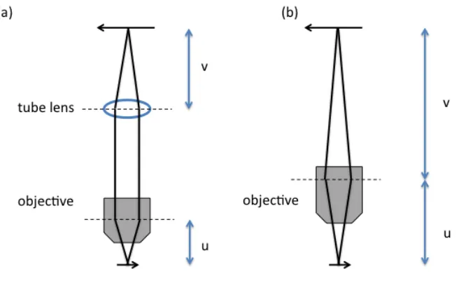
In the conventional microscope, one or more refractive lenses form an optical system, which can direct the light from the object to form a magnified image. The central part of the microscope is its objective. The objective forms the magnified real image. Figure 1.1(b) shows microcope imaging geometry with a finite optical system. The objective is attached to a body tube and then connected to a light detector such as camera film or imaging sensor at the image plane. If we would like to observe the sample with our eyes, the light detector built by Mother Nature, a pair of eyepieces is attached to the end of the body tube to form a virtual image. The microscope design has essentially remained the same since the early days of Robert Hooke [1].
Over the past decade, the major microscope manufacturers have largely migrated to infinite optical systems, as shown in Figure 1.1 (a). In infinite optical systems, the object is placed at the front focal plane of the objective, so the image distance is set to infinity, and a tube lens is placed within the body tube to produce the intermediate image [2].
Figure 1.1. The basic setup for conventional microscopes. (a) The setup for a microscope with infinite optical system. (b) The setup for a microscope with finite optical system
M
=
u
v
, (1.1)where u is the object distance, and v is the image distance. In the finite optical system, the object distance is defined as the distance between the object and the front principle plane of the objective, and the image distance is defined as the distance between the image and the back principle plane of the objective. In the infinite optical system, the object distance has the same definition as that of the finite system, while the image distance is the distance between the image and the back principle plane of the tube lens. As the object is placed in the front focal plane of the objective, and the image is formed on the back focal plane of the tube lens, the magnification of the infinite system is the ratio of the effective focal length (EFL) of the tube lens and the EFL of the objective. For example, an infinite corrected microscope objective manufactured by Nikon has an EFL of 10 mm. The EFL of a tube lens is 200 mm. Then the magnification is 200mm/10mm = 20. From these numbers we can see that the whole optical path length is on the order of tens of centimeters. This determines the size of the microscope body. In practice, an objective lens requires sophisticated design to correct for optical aberrations, and precise adjustments are needed during the assembly process. This is the reason why microscope systems are complicated and expensive.
The amount of light that can be collected by a microscope objective is limited by its physical diameter. The microscope can only accept information carried by light within a certain collection cone, and the collection range is described by the half cone angle θ. In microscopy, numerical aperture (N.A.) is more common in quantify is angle. The N.A. is defined by
N.
A.
=
n
sin
θ
, (1.2)where n is the refractive index of the imaging medium. The N.A. of a conventional microscope usually ranges from 0.05 to 1.3. Another important angle is the half field angle, ω, which describe the field of view (FOV) of the microscope objective. The relation between ω and the FOV is described as
FOV
=
2
f
tan
ω
, (1.3)where f is the EFL of the microscope objective. The half field angle of the objective is usually about 0-3°. The EFL of microscope objective is usually in the millimeter range. The common FOV of the microscope is no greater than 1 mm.
1.1.2 Improvements in resolution and contrast through novel microscopy techniques
In this section, we will discuss the resolution limits and the contrast mechanism of the conventional microscope. In recent years, the resolution and contrast has been greatly improved by new microscopy techniques. We will also briefly review some of these key improvements.
Resolution
In an aberration-free microscope system, the optical resolution is only limited by the diffraction. Based on Abbe’s equation [3], the diffraction-limited resolution, r, of a microscope is determined by,
r
=
0.61λ
N
.
A
.
, (1.4)example, for a microscope objective with 20X magnification, 0.4 N.A., the sample is illuminated with 488 nm blue light. The diffraction-limited resolution is 0.74 µm.
Recently, many optical microscopy methods have been developed to to break this diffraction limit. One of the early attempts was near field optical scanning microscopy (NSOM) [4, 5]. Recent super resolution microscopy methods aim to achieve higher resolution in the far field.
Structured illumination microscopy (SIM) [6] and 4Pi microscopy consider this diffraction limit in the spatial frequency space [7]. By using interference illumination, the two methods effectively increase the detectable frequency range in both lateral and axial directions. The lateral resolution can be doubled, and the axial resolution can be improved ~5 times.
Photo-activated localization microscopy (PALM) [8] and stochastic optical reconstruction microscopy (STORM) [9] take advantage of the photo-switchable fluorophores to selectively switch on individual fluorescent molecules and estimate the location of the molecule. The precision of the location estimation is much higher than the diffraction-limited resolution. By building a map of the locations of single emitters, a super-resolution image can be acquired. Stimulated emission depletion (STED) microscopy [10] introduces a depletion beam that controls the fluorescence emission and can create a scanning point smaller than the diffraction-limited focus.
These super resolution microscope methods allow sub 100 nanometer resolution, while still maintaining the non-invasive nature of optical imaging.
Contrast
In 1930, when Dutch Nobel laureate Frits Zernike studied optics of diffraction gratings, he realized that the direct light and the diffracted light were actually in different phases [11]. This discovery eventually led to phase contrast microscopy. Based on the same idea, differential interference contrast (DIC), has now become one of the common readout modes for the biological microscope.
Fluorescence readout is becoming one of the most significant modalities of the optical microscope, because of the sensitivity and specificity of the fluorescence molecular probe. Fluorescence is the emission of light by a fluorescence molecule that has absorbed the light of a different wavelength. In most cases, the emission has a longer wavelength than the absorbed light. Fluorescence imaging has various applications. To name a few examples: fluorescent probes against cancer markers are used for cancer diagnosis [12]; encoded fluorescent proteins enable minimally-invasive observation of gene expressions[13]; fluorophores can serve as indicators to visualize excitable cell firing and calcium transients for functional studies in neurons [14].
Furthermore, many of the super resolution techniques mentioned above require contrast from engineered fluorophores. Multi-photon absorption/emission has also led to the invention of multi-photon microscopy, which has opened a wide range of applications in deep tissue imaging [15].
Other than fluorescence, non-linear microscopy can image non-labeled samples. For example, second harmonic generation (SHG) microscopy can image the contrast provided by structures that support SHG. Stimulated Raman scattering (SRS) microscopy [16] and coherent anti-Stokes Raman spectroscopy (CARS) microscopy can image the contrast provided by vibrational frequency signatures of molecules.
1.2 Chip-scale microscope
In the previous sections we have introduced conventional microscopy and some novel microscopy techniques that improve resolution, contrast, and imaging depth. In this section we will focus on improving the microscope in another direction: bringing down the cost of the microscope.
For the past 10 years, the majority of cell phones have come equipped with a camera. The cost of the CMOS imaging sensor in cellphones is often less than $5. The invention of a mass-producible microscope will have the great potential not only to reduce the cost, but also to lead to the miniaturization of the microscope. The first on-chip microscope, the optofluidic microscope (OFM), was developed in our lab [17].
1.2.1 Optofluidic microscope
OFM exploits the time dimension during the image acquisition process. In the basic OFM setup one can imagine covering the sensor with a thin metal layer and etching a small aperture array onto the layer at the center of each sensor pixel.
Figure 1.3. Optofluidic microscope (OFM) device. (a) Imaging principle of OFM. The scale bar on the sample is 10 µm. (b) Focused ion beam image of an aperture fabricated on a CMOS sensor chip. The scale bar is 3 µm. (c) Photograph of the OFM prototype.
The resolution of an OFM is fundamentally determined by the aperture size and not the pixel size. Therefore, by choosing the appropriate aperture size, we can achieve high resolution. Figure 1.3 (b) shows the focused ion beam (FIB) image of an aperture defined on an imaging sensor coated with a 300 nm thick Al layer. Figure 1.3 (c) shows a prototype of the OFM.
Along the lines of the OFM imaging method, our group further developed other OFM models including Color OFM [18], Super-resolved OFM (SROFM) [19], and Fluorescence OFM [20].
1.2.2 Other chip-scale microscopes
Hologram microscopes are the base technology of one other family of on-chip microscopes. Nobel laureate Dennis Gabor first suggested this microscopic imaging concept with in-line holography [21]. Since the implementation of this method with an imaging sensor, the hologram-based chip-scale microscope has led to many biological applications [22, 23]. Compared with OFM methods, the hologram microscope has a large FOV and provides phase information from the sample. However, this method requires partially coherent light, and thus cannot be applied in fluorescence imaging. In addition, its phase retrieval algorithm has the assumption of sample sparcity, so it is not suitable for imaging cell cultures with high confluency.
1.3 Organization of the thesis
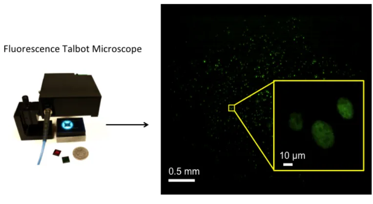
Figure 1.4. The fluorescence Talbot microscope (FTM) prototype and a large field of view image acquired by the prototype.
REFERENCES
1. R. Hooke, Micrographia or Some Physiological Descriptions of Minute Bodies (Cosimo Classics, 2007).
2. "Nikon MicroscopeU – Infinity Optical Systems,"
http://www.microscopyu.com/articles/optics/cfintro.html.
3. E. Abbe, "Beiträge zur Theorie des Mikroskops und der mikroskopischen Wahrnehmung,"
Archiv für mikroskopische Anatomie9, 413-418 (1873).
4. U. Durig, D. W. Pohl, and F. Rohner, "Near-field optical-scanning microscopy," Journal of Applied Physics59, 3318-3327 (1986).
5. E. Betzig, and R. J. Chichester, "Single molecules observed by near-field scanning optical microscopy," Science262, 1422-1425 (1993).
6. M. G. L. Gustafsson, "Surpassing the lateral resolution limit by a factor of two using structured illumination microscopy," Journal of Microscope198, 82-87 (2000).
7. S. W. Hell, S. Lindek, C. Cremer, and E. H. K. Stelzer, "Measurement of the 4pi-confocal point-spread function proves 75 nm axial resolution," Applied Physics Letters64, 1335-1337 (1994).
8. E. Betzig, G. H. Patterson, R. Sougrat, O. W. Lindwasser, S. Olenych, J. S. Bonifacino, M. W. Davidson, J. Lippincott-Schwartz, and H. F. Hess, "Imaging intracellular fluorescent proteins at nanometer resolution," Science313, 1642-1645 (2006).
9. M. J. Rust, M. Bates, and X. W. Zhuang, "Sub-diffraction-limit imaging by stochastic optical reconstruction microscopy (STORM)," Nature Methods3, 793-795 (2006).
10. K. I. Willig, S. O. Rizzoli, V. Westphal, R. Jahn, and S. W. Hell, "STED microscopy reveals that synaptotagmin remains clustered after synaptic vesicle exocytosis," Nature440, 935-939 (2006).
11. F. Zernike, "Phase contrast, a new method for the microsopic observation of transparent objects," Physica9, 686-698 (1942).
12. D. J. Brennan, D. P. O'Connor, E. Rexhepaj, F. Ponten, and W. M. Gallagher, "Antibody-based proteomics: fast-tracking molecular diagnostics in oncology," Nature Reviews Cancer10, 605-617 (2010).
13. R. Y. Tsien, L. Ernst, and A. Waggoner, "Fluorophores for confocal microscopy: photophysics and photochemistry," Handbook of biological confocal microscopy, 338-352 (2006).
14. R. Kerr, V. Lev-Ram, G. Baird, P. Vincent, R. Y. Tsien, and W. R. Schafer, "Optical imaging of calcium transients in neurons and pharyngeal muscle of C. elegans," Neuron26, 583-594 (2000).
15. W. Denk, J. H. Strickler, and W. W. Webb, "Two-photon laser scanning fluorescence microscopy," Science248, 73 (1990).
16. C. W. Freudiger, W. Min, B. G. Saar, S. Lu, G. R. Holtom, C. W. He, J. C. Tsai, J. X. Kang, and X. S. Xie, "Label-free biomedical imaging with high sensitivity by stimulated Raman scattering microscopy," Science322, 1857-1861 (2008).
17. X. Cui, L. M. Lee, X. Heng, W. Zhong, P. W. Sternberg, D. Psaltis, and C. Yang, "Lensless high-resolution on-chip optofluidic microscopes for Caenorhabditis elegans and cell imaging,"
Proceedings of the National Academy of Sciences105, 10670 (2008).
19. G. Zheng, S. A. Lee, S. Yang, and C. Yang, "Sub-pixel resolving optofluidic microscope for on-chip cell imaging," Lab on a Chip10, 3125-3129 (2010).
20. S. Pang, C. Han, L. M. Lee, and C. H. Yang, "Fluorescence microscopy imaging with a Fresnel zone plate array based optofluidic microscope," Lab on a Chip11, 3698-3702 (2011).
21. D. Gabor, "A New Microscopic Principle," Nature161, 777-778 (1948).
22. A. Ozcan, and U. Demirci, "Ultra wide-field lens-free monitoring of cells on-chip," Lab on a Chip8, 98-106 (2008).
23. W. Bishara, T.-W. Su, A. F. Coskun, and A. Ozcan, "Lensfree on-chip microscopy over a wide field-of-view using pixel super-resolution," Optics Express18, 11181-11191 (2010).
C h a p t e r 2
COLOR OPTOFLUIDIC MICROSCOPE
In the previous chapter we have briefly reviewed some new effort in redesigning the microscope for low-cost and compact devices. In this chapter, we describe the implementation of a color-capable on-chip lensless microscope system, termed color optofluidic microscope (color OFM), and demonstrate imaging of double stained Caenorhabditis elegans (C. elegans) with lacZ gene expression. This chapter is adapted from S. Pang, X. Cui, J. DeModena, Y. M. Wang, P. W. Sternberg, and C. Yang, "Implementation of a color-capable optofluidic microscope on a RGB CMOS color sensor chip substrate", Lab on a Chip10, 411-414 (2010).
2.1 Introduction
The development of microscopes that are autonomous, compact, low-cost and high-resolution can improve existing microscopy applications in point-of-care diagnostics, and potentially engender new microscope usage. The lensless and fully on-chip microscope systems, termed the optofluidic microscopes (OFM), as briefly reviewed in the last chapter, can potentially fill this role. [1, 2]
Cell color staining is a common technique for better visualization of tissue or cells in bright field microscopy. By using different stains, one can preferentially stain specific cell components. Color staining is useful for the observation of particular metabolic processes or the differentiation between live and dead cells. Some examples of commonly used color stains are: hematoxylin, a nuclear stain that stains nuclei blue-violet; iodine, a starch indicator; Trypan blue, a vital stain that selectively colors dead tissues or cells; and nile red, which stains intracellular lipid globules red.
The capability to image a color sample using OFM will enrich more applications for on-chip imaging. In this Chapter, we present an OFM system that is capable of performing color imaging. This system uses a color CMOS sensor chip in place of a monochromatic CMOS sensor chip in the standard OFM, and employs an aperture array arrangement that accommodates the Bayer color pixel arrangement on such sensors.
concentration of a dye, Trypan Blue, under varying illumination intensity. Finally, we will show color OFM images of the microscopic nematode C. elegans expressing β-galactosidase with a blue LacZ stain, and Ponceau, a nonspecific red stain.
2.2 Imaging principles of color OFM
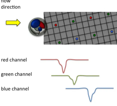
As briefly mentioned in Chapter 1, OFM method utilizes microfluidic flow to transport samples across one or more arrays of small apertures (1 micron or smaller) on a metal-coated CMOS imaging sensor that is illuminated with light. The passage of a sample interrupts light transmission through the apertures, and the time-varying transmission associated with each aperture effectively represents a line trace across the sample.
Figure 2.1. Imaging principle of the color OFM based on a color imaging sensor. Each aperture corresponds to a color channel.
By appropriately compositing these line traces from these apertures, we can then generate a high-resolution image of the sample at a high-resolution comparable to the aperture size. The diagonal arrangement of the aperture array across the channel floor allows the aperture arrays to fully scan a sample flowing in the channel.
green, and blue channels. Figure 2.1 shows the schematic plots of the color OFM. So instead of collecting the signal from one line of aperture array, two aperture arrays collect the light from the three different color channels. A RGB image can be acquired by combining the color channels together.
The absence of lenses and other bulk optical elements in the OFM design is particularly advantageous as it allows us to implement highly compact chip-scale microscope systems that are mass-producible in a semiconductor foundry. In addition, as the OFM can directly process samples in fluid media, this method eliminates the need to prepare fluid samples onto a glass slide for standard microscopy examination. The basic OFM design can be altered to provide additional imaging capability.
2.3 Color OFM device fabrication
The color OFM prototype was fabricated on a color CMOS sensor substrate; the sensor (Aptina, MT9T001P12STC) consists of 2048 × 1536 pixels of size 3.2 µm. Each of these pixels is coated with one of three different chromatic filters that nominally transmit the red (R), green (G) or blue (B) region of the optical spectrum. The color pixels are arranged in a two by two Bayer pattern consisting of two diagonal green pixels, one red pixel and one blue pixel as shown in Figure 2.2(a).
We spin-coated a polymethyl methacrylate (PMMA) layer of 300 nm in thickness to planarize the sensor’s surface.
Figure 2.3. Focused ion beam (FIB) image of the sensor pixels coated with aluminum of different planarization layer thicknesses. (a) No PMMA. (b) 300 nm PMMA. (c) 600 nm PMMA.
We next used a metal evaporator with thermal source (CHA Industries, Mark 40) to deposit a 300 nm thick aluminum layer on top of the PMMA layer. By choosing the correct photoresist thickness (300 nm), we were able to discern the pixel reliefs on the chip. Figure 2.3 shows the CMOS sensor pixel with different PMMA thicknesses. At 300 nm thicknesses, the outlines of individual pixels were still discernible under SEM imaging and the surface was sufficiently flat to allow subsequent bonding of a PDMS block containing a microfluidic channel onto the chip. We then used a focused ion beam (FIB) machine (FEI Company, Nova200) to mill two arrays of 140 apertures on the aluminum layer. Then another 200 nm PMMA layer was spin coated on the aluminum layer to protect the aperture. The diameter of the aperture was 0.7 µm. The apertures were spaced 9.6 µm apart (equal to 3-pixel pitch). The two arrays were also spaced 9.6 µm apart. The relatively wide spacing choice was made to minimize crosstalk effects from neighboring pixels. We took care to ensure that the apertures were each milled directly above a single sensor pixel by exercising a good control over the milling process. The apertures of the first and second array were patterned over the color pixels in repeating sequence of –RG- and –GB- respectively. Figure 2.2 (b) shows the aperture arrangement for the color OFM device.
across the width of the channel. The cross-section view and a photo of the final device are shown in Figure 2.4.
Figure 2.4. Color OFM device. (a) The illustration of the cross-section view of gravity driven color OFM setup. (b) The color OFM device compared with a microscope objective.
The system was uniformly illuminated with light (~10 mW/cm2) from a halogen lamp. We programmed the sensor to specifically read signals from the two lines of pixels directly below the aperture arrays. The readout rate was 1.3 kHz/s. The time-varying transmission change measured through each aperture represents a line scan of a sample passing through the microfluidic channel. By stacking the line scans from the apertures together, we can then generate an image of the sample. Based on the aperture size, we have previously established that such a system has a resolution of 0.8 µm at its plane of highest acuity (bottom of the channel) [3].
2.4 The effect of the aperture on the color pixels
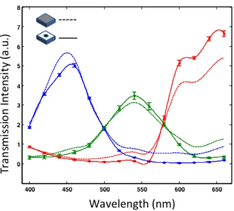
Figure 2.5. The small aperture effect on spectral response of the color sensor. The solid line are the measured transmission data from a color OFM device. The dash lines are the response from a CMOS sensor without any fabrication process.
Figure 2.5 shows the spectral response for the red, green, and blue pixels from the OFM device and compares it with an unprocessed color CMOS sensor. The results show that the blue and green pixels’ spectral responses were slightly impacted by presence of the apertures while the red pixel showed some deviations. The impact is sufficiently moderate and positively indicates that our fabrication procedures did not significantly degrade the chromatic filters on the pixels. This set of data is helpful in aiding us renormalize the OFM measurements.
One of the advantages of color imaging is that the multi-spectral information can be used to quantify the relative concentration of the dye used in stained samples. For example, the optical signal detected by a blue pixel can be mathematically expressed as:
)
exp(
nl
T
T
b=
bo−
σ
b , (2.1)where Tbo is the optical signal detectable in the absence of a sample, σb is the dye’s absorption
spectral variation is known, we can determine the dye concentration by making four measurements: Tb, Tbo, Tr, and Tro. The dye concentration can then be calculated from:
l
T
T
T
T
n
b g bo ro r b)
(
)
ln(
)
ln(
σ
σ
−
−
=
, (2.2)
from which we can see the linear relationship between ln(Tb/Tr) and the slope is independent of the
illumination intensity, Tbo and Tro. In this example, we chose the red and blue pixels as the target
pixel pair. We can alternately pick any paired combination of the three color-pixels. Ideally, we should pick the color pixel associated with the largest dye absorption cross-section and the color pixel associated with the smallest dye absorption cross-section to maximize sensitivity.
To verify this capability, we flowed a blue dye, Trypan Blue, at varying concentration through a color OFM system. The microfluidic channel was 28 µm in height. The illumination intensity was 4 mW/cm2. We varied the Trypan Blue concentration from 0 to 1.2 mM in 0.2 mM increments. The
Tb andTr measurements were acquired with pixels directly underneath the channel while the Tb0and
Tro measurements were acquired from pixels that were not covered by the channel. The result
shown in Figure 2.6 verifies that the measured ratio ln(Tb/Tr) is a linear function of the dye
concentration. To verify that this ratio is independent of the illumination intensity, we repeated the experiment at a higher illumination intensity of 6 mW/cm2 by increasing the power of the halogen lamp. Figure 2.6 shows that the measured ratio overlapped with that of the original experiment.
2.5 Color imaging of C. elegans
Next, we demonstrated our prototype by imaging C. elegans with for LacZ expression. The LacZ (β-galactosidase) gene is frequently used as a reporter in some bacterial-based selection techniques [4]. The location where LacZ is expressed can be easily located with a LacZ stain containing the artificial substrate X-gal, which turns blue when it is cleaved by β-galactosidase.
The C. elegans (pPD82.51) strain used contains a myo-2::lacZ fusion, which when expressed, stains the pharyngeal muscles of the worm’s head blue after treatment with the X-gal, purchased from
Caenorhabditis Genetics Center. The worms were fixed at their early larval stage L-1. We used the Lac Z Tissue Staining Kit (rep-lz-t, InvivoGen) for staining, and followed the protocol. In addition, we stained the worms with Ponceau-S, a stain commonly used to visualize proteins on Western blots, as a method of obtaining a second color, red, simultaneously on each worm. The stained worms were resuspended in 1 × PBS with a concentration about 10 worms/µL.
By operating the color OFM on an inclined plane, we were able to induce the C. elegans worms to flow through the microfluidic channel via gravitational pull. The transportation velocity ranged from 500 µm/s to 1000 µm/s. As in our previous experiments, we used the same halogen lamp as our light source. At this speed range and sensor readout speed, we could sample the worms in less than 0.5 µm intervals along the flow channel direction. This ensured adequate sampling and ensured that the image resolution was limited by the aperture size [1].
Figure 2.7. Reconstruction of a color OFM image of C. elegans with LacZ expression. (a)-(c) From top to bottom are the images from red, green, blue pixels of a C. elegans with blue Xgal stain and ponceau stain image, (d) the constructed color OFM image shows the nonspecific ponceau stain (left arrow) and the LacZ staining of the pharyngeal muscles (right arrow), (e) the conventional 10X microscope image of the same sample. The scale bar is 20 microns.
Figure 2.8. The comparison between the color OFM image and the monochromatic image. The scale bar is 20 microns.
As this color OFM design is microfluidic based, it can form part of a greater microfluidic analysis system in which sample prep and staining are all performed on chip. It is also possible to envision more sophisticated staining and imaging strategies in order that such a compact imaging system could be used optimally. For example, the color OFM can be used to automatically image samples that are sequentially stained with different dyes, in which imaging is performed after each staining step. Such a scheme is difficult to automate in a conventional laboratory, but is relatively simple to implement in a well-controlled microfluidic system [5].
2.6 Conclusion
REFERENCES
1. X. Q. Cui, L. M. Lee, X. Heng, W. W. Zhong, P. W. Sternberg, D. Psaltis, and C. H. Yang, "Lensless high-resolution on-chip optofluidic microscopes for Caenorhabditis elegans and cell imaging," Proceedings of the National Academy of Sciences of the United States of America 105, 10670-10675 (2008).
2. X. Heng, D. Erickson, L. R. Baugh, Z. Yaqoob, P. W. Sternberg, D. Psaltis, and C. H. Yang, "Optofluidic microscopy - a method for implementing a high resolution optical microscope on a chip," Lab on a Chip6, 1274-1276 (2006).
3. X. Heng, X. Q. Cui, D. W. Knapp, J. G. Wu, Z. Yaqoob, E. J. McDowell, D. Psaltis, and C. H. Yang, "Characterization of light collection through a subwavelength aperture from a point source," Optics Express14, 10410-10425 (2006).
4. J. K. Joung, E. I. Ramm, and C. O. Pabo, "A bacterial two-hybrid selection system for studying protein-DNA and protein-protein interactions," Proceedings of the National Academy of Sciences of the United States of America97, 7382-7387 (2000).
C h a p t e r 3
FRESNEL ZONE PLATE BASED FLUORESCENCE OPTOFLUIDIC MICROSCOPE
In the previous chapters, we have introduced the imaging principles and implementation of bright field/color optofluidic microscopes (OFM). In this chapter we report the implementation of an on-chip fluorescence microscope system, termed fluorescence optofluidic microscope (FOFM). This device is capable of fluorescence microscopy imaging of samples in fluid media. The FOFM employs an array of Fresnel zone plates (FZP) to generate an array of focused light spots within a microfluidic channel. As a sample flows through the channel and across the array of focused light spots, the fluorescence emissions are collected by a filter-coated CMOS sensor, which serves as the channel's floor. The collected data can then be processed to render fluorescence microscopy images at a resolution determined by the focused light spot size (experimentally measured as 0.65 µm FWHM). In our experiments, our established resolution was 1.0 µm due to Nyquist criterion consideration. As a demonstration, we show that such a system can be used to image the cell nuclei stained by Acridine Orange and cytoplasm labeled by Qtracker®. This Chapter is adapted from S. Pang, C. Han, L. M. Lee, and C. H. Yang, "Fluorescence microscopy imaging with a Fresnel zone plate array based optofluidic microscope", Lab on a Chip11, 3698-3702 (2011).
3.1 Introduction
In the past few years, there has been significant research and development in the area of bright field chip-scale microscopy [1, 2]. An inexpensive, highly compact and easy-to-use chip-scale microscope can be an important lab-on-a-chip component for point-of-care medical systems, low-cost diagnostic tools for developing country applications, and high-throughput automated bioscience analysis systems. A high-resolution and generally usable fluorescence on-chip microscopy technique can significantly expand the utility range of such chip-scale microscopes. The high sensitivity of the fluorescence signal detection and the broad array of fluorophore species and expression techniques available make fluorescence one of the most important read-out modes for microscopy [3].
Coskun et al. show that it is possible to superpose an indication of the fluorophore concentration sites onto brightfield in-line holography derived images of samples as long as the fluorophores are clustered and the clusters are well separated (by ~ 10 µm) [4]. A progression of that effort uses bundled fibers to collect and channel fluorescence to a sensor and was able to generate fluorescence images that have a claimed resolution of ~ 4 µm [5]. Improving the technique's resolution to the point where sub-cellular fluorescence features are resolvable may prove challenging as finer fiber tips will further diminish the effective fluorescence collection angle and the light channeling efficiency.
In this chapter, we report a chip-scale imaging method, termed “fluorescence optofluidic microscope” (FOFM), which adapts the scan-based imaging strategy of the optofluidic microscopy method to accomplish high-resolution fluorescence microscopy imaging. Compared with aperture based on-chip imaging platform [2], this approach is highly efficient at fluorescence light collection. It is also capable of placing the plane of highest acuity at any desired height within the sample and its resolution can be adjusted by a straightforward alteration of its design parameters. Our FOFM prototypes were able to achieve 0.60 µm FWHM at the focused spot for excitation wavelength of 405 nm and 0.65 µm FWHM for 488 nm excitation. The FOFM is suitable for mass-manufacture in a semiconductor foundry, and therefore FOFM devices have the potential to be made very compactly and cost-effectively.
In the following section, we will describe the FOFM's imaging principle. Then, we will describe the fabrication steps involved in our prototype construction. Next, we will discuss our characterization of the experimental results and report on our demonstration experiments that use our prototypes for fluorescence microscopy imaging of cells.
3.2 Fluorescence optofluidic microscope (FOFM) 3.2.1 Imaging principle
Figure 3.1. Schematics of the Fresnel zone plate based fluorescence opto-fluidic microscope (FOFM). A sample flows in the microfluidic channel on top of the filter coated image sensor. The Fresnel zone plate array creates an array of foci inside the channel.
As a sample flows through the channel, each focused light spot will locally excite fluorophores within the sample. The fluorescence signal collection is accomplished by a low-cost CMOS sensor, which is coated with a filter that effectively blocks the excitation light and that efficiently transmits fluorescence emissions well. The time varying fluorescence signal associated with each spot represents a single line scan across the sample. Figure 3.2 shows the geometry of the FZP arrangement. The FZP array spans the channel diagonally such that the distance between the adjacent scan lines is less than the FWHM of the PSF of each focus. This assures that we can fully scan all parts of the sample and that by appropriately compositing all line scans, we can then generate a high-resolution fluorescence image of the sample at a resolution that is limited by the focused spot size.
Figure 3.2. Geometry of the FOFM device (top view). The Fresnel zone plates are defined on the top floor of the microfluidic channel and span across the whole microfluidic channel (blue region).
3.2.2 Fresnel zone plate
For each of our FOFM prototypes, we fabricated the FZP array on a 300 nm thick chrome layer that was plated on a quartz substrate. Each FZP was composed of a series of transparent and opaque concentric rings [6]. Figure 3.3 (a) illustrates the FZP focusing.
Figure 3.3. Fresnel zone plate (FZP) focusing. (a) The illustration of the FZP focusing (b) SEM image of a binary FZP patterned on a chrome mask.
To create the focus at a focal length f the zones should switch from opaque to transparent at radii
€
rk= kf λ
n+ k2
λ2 4n2
where k is an integer, λ is the wavelength of the light and n is the refractive index of the medium in which the focus is formed. The resolution, δ, of a focal spot of a zone plate depends on the smallest zone width [6]
€
δ =1.22ΔrK
,
(3.2)where ΔrK is the outer most zone width, which is determined by the fabrication limit. In our case,
the FZP pattern was defined by electron beam lithography with a minimum achievable line width of 400 nm. The depth of the focus Δ [7], defined the half distance between two adjacent axial intensity minima of a FZP focus, can be calculated as
€
Δ
=
f
/
N
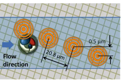
, (3.3)where N is the number of transparent zones, which is five in our design. Figure 3.3 (b) shows a scanning electron microscopy image of a single FZP in our prototypes. The distance between each FZP was 20.8 µm - this corresponds to the length of four sensor pixels on the CMOS sensor. The designed focal length was 13 µm and the diameter of each FZP was 15 µm. The exact FZP ring parameters were governed by Equation 3.1 and they differed between the two groups of FOFM prototypes we implemented. One group was designed to work at an excitation wavelength of 405 nm and the other at an excitation wavelength of 488 nm.
3.2.3 Device fabrication
Figure 3.4. FOFM device. (a) The schematics of the FOFM device. (b) The photograph of two FOFM prototypes with green and red filter layers placed besides a US dime to show their size.
Figure 3.5. The transmission spectrum of 6 µm thick red filter layer and 8 µm thick green filter layer. The arrows indicate the emission peaks of Acridine Orange and Qdot 625. The 405 nm and 488 nm excitation lines are also marked for reference. The transmission measurement is done at 1.5 µm thickness. The OD number at 6 and 8 µm are calculated results.
3.3 Resolution of the FOFM
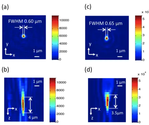
To verify the focus quality, we observed the focus formed by the FZP by a 40X 0.85 N.A. water immersion microscope objective. Here we used the water immersion microscope objective to match the refractive index of the medium in the microfluidic channel. A piece of the top plate with FZP arrays was mounted on a vertical motorized stage. The stage moved with a step size of 0.5 µm, and a camera captured images of the focus at each step. Figure 3.6 shows the experimental results. The FWHM of the focus was 0.60 µm for 405 nm excitation, and 0.65 µm for 488 nm excitation, which were slightly larger than the theoretical value of 0.5 µm. The focal depth for the 405 nm version was 4.0 µm, and the focal depth for the 488 nm version was 3.5 µm.
Figure 3.6. The intensity profile of the focus generated by FZP. (a) The intensity of the focus at the focal plane by 405 nm excitation. (b) The depth-wise cross-section of the intensity of the focus by 405 nm excitation. (c) The intensity of the focus at the focal plane by 488 nm excitation. (d) The depth-wise cross-section of the intensity of the focus by 488 nm excitation.
3.4 Fluorescence imaging with the FOFM prototype
In our demonstration a 488 nm laser (Cyan OEM488 nm, Spectra-Physics) and a 405 nm laser (OEM Laser System Inc.) were used as the excitation sources for the FOFM. The power at each FZP generated focal spot was about 10 µW. During operation, the imaging frame rate was 1 kHz.
frames of low-resolution bright field images of sample flowing through that segment of the microfluidic channel. These images could then be processed to form a higher-resolution image by using the sub-pixel resolving OFM (SROFM) method described in [10].
The SROFM method's resolving ability degrades as a function of sample-to-sensor separation. Since the FOFM sensor chips were coated with a ~13 µm thick layer of filter material and PDMS material, the acquired SROFM images are relatively low in resolution. Nevertheless, they could be used to provide outlines of the samples imaged. In applications where high-resolution brightfield microscopy images are required, the on-chip microscope can be designed to exclude the filter material from the SROFM portions of the sensor chip.
3.4.1 FOFM imaging of fluorescence microspheres
Figure 3.7 Microsphere imaging by FOFM. (a) A line trace of a fluorescence microspheres by a single FZP, comparing to the calculation result. (b) The fluorescence image of a fluorescence microsphere collected by FOFM. (c) The fluorescence image of a fluorescence microsphere by direct readout from the sensor with uniform illumination.
3.4.2 FOFM imaging of fluorescently labeled HeLa cells
Figure 3.8. Fluorescence images of stained HeLa cells collected by FOFM. (a1-a3) The fluorescence images of Acridine Orange stained HeLa cells acquired by FZP FOFM superimposed on defocused bright field SROFM images to provide the outline. (b1-b3) The fluorescence images of Qtracker labled HeLa cells acquired by FZP FOFM superimposed on defocused bright field SROFM images. (a4, b4) The fluorescence image superimposed on a bright field image acquired by a conventional 20X 0.4 N.A. microscope.
The flow speed was approximately 500 µm/s, and the frame period was 1 ms, corresponding to the displacement of 0.5 µm per frame. Each sample’s flow speed uniformity was monitored by the SROFM segments of the prototypes, and the yield rate was comparable to those of earlier OFM systems [1]. The green filter coated FOFM captured images of the Acridine Orange stained cells, and the red filter coated FOFM captured images of the Qtracker® stained cells. The fluorescence images captured by FOFM prototypes were superimposed with the super-resolution bright field images. Figure 3.8 (a1-a3) shows images of the HeLa cell nuclei stained by Acridine Orange. The fluorescence signal is concentrated within the center of a cell. Figure 3.8 (b1-b3) shows the images of the HeLa cytoplasm labeled by Qtracker®. The Qtracker contrast agents are non-specific-binding quantum dots. The Qtracker stain pattern is expected to vary from cell to cell. We also acquired images with a conventional microscope operating with a 20X 0.4 N.A. objective for comparison (Figure 3.8 (a4) and (b4)). We can see that the fluorescence images acquired with the FOFM prototypes agree with those acquired with a conventional fluorescence microscope.
micron to our fluorescence images due to Nyquist sampling criterion considerations [12]. To achieve the resolution set by the FZP's focused spot size, we would need to increase the sampling frame rate and increase the line scan overlap.
3.5 Discussion
In this section, we would like to point out several features of our FOFM design and the potential improvments.
First, the choice of using a filter coated CMOS sensor to serve as the device's floor carries two advantages. Specifically, we can optimally collect fluorescence from the sample without requiring the use of a more elaborate collection optics scheme. The FOFM design can collect almost all fluorescence from the bottom semisphere of an isotropic fluorescence source, which is close to 50% of the total emission. In contrast, a 0.65 N.A., 40X microscope objective is only able to collect ~12% of the total emission. In addition, this simple planar and monolithic collection design is very compatible with semiconductor mass-manufacture.
Another noteworthy point of this FOFM design is that, by spacing the FZP apart from each other at an adequate distance, it is possible to separate the detected fluorescence associated with each focused spot by the CMOS sensor without ambiguity. More interestingly, if the approximate size of the sample is known, we need only space the FZP at a distance larger than the sample size to guarantee that cross-talk is absent - in this case, only one focused spot can interrogate the sample at any given time and any signal we see on the sensor can be automatically attributed to that focused spot. In fact, our FOFM prototypes made good use of this design point. A thick layer of filter material and PDMS separates the sensor pixels from the channel: the overall thickness is about 13 microns. The fluorescence from a fluorophore in the center of one of the focused light spots would spread over an area of diameter at least 30 µm (or 6-7 sensor pixel lengths) on the sensor. This implies that at our FZP-to-FZP distance of 20.8 µm, fluorescence signals associated with adjacent focused light spots could overlap and contribute cross-talk to each other. The cells used in our experiments are less than 20 µm in diameter and, as such, only one focused light spot can excite a given cell at anytime and we were able to avert cross-talk problems. To work with large cells or samples, we simply would need to increase the FZP-to-FZP distance.
mass-manufacture. This is a relevant consideration as we envision the mass-manufacture of OFM would occur in semiconductor foundries. Further more, the FZP approach allows for the generation of tight focus spots with short focal length that would be very difficult to accomplish with a refractive optical element. As a case in point, if we were to replace one of the FZP elements in our prototype with a ball lens of the same diameter, the ball lens would have to possess a refractive index of at least 2.7 (in comparison to quartz glass, which has a refractive index only 1.45 in the optical band) to achieve the same focal length. The FZP approach does come at a flexibility price, since the focal length of the FZP depends strongly on the optical wavelength. As such, each FOFM needs to be designed with a specific excitation wavelength in mind. Finally, our current FZP is able to direct ~10% of the incident light into the focused spot. If application requirements demand higher efficiency, the current binary FZP can be switched to a binary phase FZP, which has 40.4% (4/π2) efficiency, or a Fresnel lens, which in principle can reach 100% efficiency.
3.6 Conclusion
REFERENCES
1. X. Cui, L. M. Lee, X. Heng, W. Zhong, P. W. Sternberg, D. Psaltis, and C. Yang, "Lensless high-resolution on-chip optofluidic microscopes for Caenorhabditis elegans and cell imaging,"
Proceedings of the National Academy of Sciences of the United States of America105, 10670 (2008).
2. S. Pang, X. Cui, J. DeModena, Y. M. Wang, P. Sternbergc, and C. Yangab, "Implementation of a color-capable optofluidic microscope on a RGB CMOS color sensor chip substrate," Lab on a Chip10, 411-414 (2010).
3. R. Y. Tsien, L. Ernst, and A. Waggoner, "Fluorophores for confocal microscopy: photophysics and photochemistry," Handbook of biological confocal microscopy, 338-352 (2006).
4. A. F. Coskun, I. Sencan, T. W. Su, A. Ozcan, and E. Mylonakis, "Lensfree Fluorescent On-Chip Imaging of Transgenic Caenorhabditis elegans Over an Ultra-Wide Field-of-View," PloS one6, 896-903 (2011).
5. A. F. Coskun, I. Sencan, T. W. Su, and A. Ozcan, "Wide-field lensless fluorescent microscopy using a tapered fiber-optic faceplate on a chip," Analyst (2011).
6. M. Young, "Zone plates and their aberrations," Journal of Optical Society of America62, 972-976 (1972).
7. M. Sussman, "Elementary diffraction theory of zone plates," American Journal of Physics28, 394 (1960).
8. Y. Xia, and G. M. Whitesides, "Soft lithography," Annual Review of Materials Science28, 153-184 (1998).
9. M. Heckele, and W. K. Schomburg, "Review on micro molding of thermoplastic polymers,"
Journal of Micromechanics and Microengineering14, R1 (2004).
10. G. Zheng, S. A. Lee, S. Yang, and C. Yang, "Sub-pixel resolving optofluidic microscope for on-chip cell imaging," Lab on a Chip10, 3125ñ3129 (2010).
11. N. Umezawa, M. A. Gelman, M. C. Haigis, R. T. Raines, and S. H. Gellman, "Translocation of a -peptide across cell membranes," Journal of the American Chemical Society124, 368-369 (2002).
C h a p t e r 4
FLUORESCENCE TALBOT MICROSCOPY
This chapter intends to provide an overview of a fluorescence microscope based on the Talbot effect. In the previous chapter, we have described the implementation of a fluorescence on-chip imaging device based on OFM methods. In addition to the cost-effectiveness and compactness associated with on-chip microscopy, the fluorescence Talbot microscope (FTM) method explores the possibility of achieving wide field-of-view (FOV) and high collection efficiency. The chapter starts with a brief review of the methods used to achieve wide FOV in fluorescence microscopy, particularly by focal spot array scanning microscopy for high-speed imaging. Next we will give a brief introduction of the Talbot effect and some of its key properties, which serve as the foundations for the FTM method. In the third section, we will describe the working principle of the FTM and report an implementation of the on-chip prototype of the FTM. Finally we will show the fluorescence microscopy images acquired by the on-chip FTM prototype.
The characterization of the on-chip FTM will be described in Chapter 5, and in Chapter 6 we use the Talbot microscope method in imaging samples labeled with two different fluorescence stains. In Chapter 7 we will report two biological applications using the FTM. Chapter 8 will discuss the potentials and the outlook for FTM methods.
4.1 Wide FOV microscopy
4.1.1 Conventional microscope achieving wide FOV
The conventional microscope has limited FOV due to the constraints of the available optical material and design. One possibility to increase the FOV of the microscope is to increase the physical aperture of the microscope. However the aberration also increases if one just simply scales up the optical design. If the aberration is compensated for, the design becomes complicated and the cost of the system increases. Such large aperture lenses are used in photolithography lenses [1], and are not suitable for a biology laboratory.
microscope's FOV to increase the throughput. Figure 4.1 shows a microscope slide scanner based on this method. However, the inclusion of a conventional microscope precludes system parallelization that could otherwise bring orders-of-magnitude throughput improvements.
Furthermore, there are certain applications, such as living cell time-lapse imaging, where photo-bleaching and photo-toxicity are major concerns [5]. In these situations, users typically have to trade-off a larger FOV against increased light collection efficiency by resorting to a high magnification microscope objective, which increases the imaging time and the system cost.
Finally, the time spent on the step motion and focus readjustment is longer than the imaging time. State-of-art commercialized slide scanners use time delayed integration (TDI) cameras, so that a continuous scan can be applied in one scan direction, while the step movement is still required in the other direction [6]. This effort can reduce the full field imaging time, yet the TDI camera is not common in most labs.
Figure 4.1. Wide FOV achieved by a conventional microscope. An example of digital slide scanner by Hamamatsu, where a motorized stage translates the slides under the microscope objective’s FOV. Figure courtesy of Ref [6].
Chip-scale fluorescence microscopes can potentially provide a wide FOV. In chip-scale microscope devices, the FOV is limited by the imaging sensor size, which is ~100 times larger than the FOV of a 20X microscope objective. Among the existing chip-scale microscope designs, the hologram method is not feasible, because of the non-coherent nature of the fluorescence signal. In a reported lens-less microscopy, which is based on post digital processing, the fluorescence point spread function (PSF) needs to be measured. Then deconvolution and compressed sensing are applied to the defocused fluorescence image to calculate the position and intensity of the fluorophore [7]. This method fails when the PSF is modified [8], as in the common cases where the fluorophore is out of the calibration plane, or there are scattering samples in the vicinity of the fluorophore. Moreover, the algorithm assumption limits the applications to only sparse fluorophore distribution [9].
Figure 4.2. The comparison between on-chip detection and detection using a relay lens.
Because of the distance from the sample to the imaging sensor, the fluorescence spreads out on the sensor, and the PSF is usually on the order of 10-100 µm. Figure 4.2 shows this collection geometry compared with collection using imaging optics. As a result, the achievable resolution is only ~10 µm, for on-chip detection.
achieve high resolution [10]. FOFM provides resolutions as high as 1.0 µm, but it places limitations on the sample size, as the sample was translated in a microfluidic channel.
4.1.3 Focal spot grid scanning microscope
Instead of translating the sample as in the FOFM method, alternatively, we can translate the focal array to scan the sample. Recent works have demonstrated the use of point scans to improve the scanning speed in microscope systems [11-14]. In t