Image PUF: A Physical Unclonable Function for
Printed Electronics based on Optical Variation of
Printed Inks
Ahmet Turan Erozan, Michael Hefenbrock, Michael Beigl,
Jasmin Aghassi-Hagmann, and Mehdi B. Tahoori,
Senior Member, IEEE
Abstract—Printed Electronics (PE) has a rapidly growing market, thus, the counterfeiting/overbuilding of PE components is anticipated to grow. The common solution for the counterfeiting is Physical Unclonable Functions (PUFs). In PUFs, a unique finger-print is extracted from (irreproduceable) process variations in the production and used in the authentication of valid components. Many commonly used PUFs are electrical PUFs by leveraging the impact of process variations on electrical properties of devices, circuits and chips. Hence, they add overhead to the production which results in additional costs. While such costs may be negligible for many application domains targeted by silicon-based VLSI technologies, they are detrimental to the ultra-low-cost PE applications. In this paper, we propose an optical PUF (iPUF) extracting a fingerprint from the optically visible variation of printed inks in the PE components. Since iPUF does not require any additional circuitry, the PUF production cost consists of merely acquisition, processing and saving an image of the circuit components, matching the requirements of ultra-low-cost margin applications of PE. To further decrease the storage costs for iPUF, we utilize image downscaling resulting in a compression rate of 484x, while still preserving the reliability and uniqueness of the fingerprints. The proposed fingerprint extraction methodology is applied to four datasets for evaluation. The results show that the process variation of the optical shapes of printed inks is suitable as an optical PUF to prevent counterfeiting in PE.
Index Terms—Printed Electronics, Disposables, Low-cost, Op-tical PUF, Anti-Counterfeiting, Security, Authentication, Identi-fication, Fingerprint.
I. INTRODUCTION
Printed Electronics (PE) is a promising candidate to en-able applications where ultra-low-cost, on-demand fabrication, and/or mechanical flexibility are required. PE provides these features owing to its additive and point-of-use manufacturing as well as the usage of various substrate types [1]. Therefore, several envisioned applications such as smart packaging [2],
A. T. Erozan is with the Chair of Dependable Nano Computing, Karlsruhe Institute of Technology, 76131 Karlsruhe, Germany, and also with the Institute of Nanotechnology, Karlsruhe Institute of Technology, 76344 Eggenstein-Leopoldshafen, Germany (e-mail: [email protected]).
M. Hefenbrock and M. Beigl are with the Chair of Pervasive Computing Systems-TECO, Karlsruhe Institute of Technology, 76131 Karlsruhe, Germany (e-mail: [email protected]; [email protected]).
J. Aghassi-Hagmann is with the Institute of Nanotechnology, Karlsruhe Institute of Technology, 76344 Eggenstein-Leopoldshafen, Germany, and also with the Department of Electrical Engineering and Information Technology, Offenburg University of Applied Sciences, 77652 Offenburg, Germany (e-mail: [email protected]).
M. B. Tahoori is with the Chair of Dependable Nano Computing, Karlsruhe Institute of Technology, 76131 Karlsruhe, Germany (e-mail: [email protected]).
in-situ monitoring for logistics [3], health monitoring patches [4], [5], smart cards [6], smart labels [7], pharmaceuticals [8] and disposable food sensors [9] can benefit from the features of PE.
Counterfeiting is a major problem in the domain of in-tegrated circuits and systems, automotive parts, software, cosmetic, jewellery, health-care diagnosis systems, and drugs [10], [11], [12], [13]. Since PE has a huge market, projected to grow from $29B in 2017 to $73B in 2027 [14], [15], the counterfeiting of PE components has been expected to rise, and technology-specific, low-cost measures have to be taken [16].
Physical Unclonable Functions (PUFs), which generate bio-metric fingerprints from manufacturing variation, have been utilized to prevent counterfeiting [13], [17], [18]. Electrical PUFs and optical PUFs are two distinctive examples in various fields [18], [19], [20]. Recently, the optical PUFs has received an increasing interest since they can generate the fingerprint based on visual inspection and image processing without adding a physical overhead to the product [18], [19], [20], [21]. This is beneficial for low-cost applications where adding an additional physical tag is infeasible for economic reasons. On the other hand, it is important to develop an image processing based fingerprint extraction methodology which generates fingerprints while considering their storage costs, particularly for high volume products.
In this work, we propose an optical PUF, namely image PUF (iPUF), for the anti-counterfeiting and identification of ultra-low-cost PE systems. The proposed methodology extracts fingerprints from the optically visible variations of printed inks used during manufacturing process of PE circuits, so that no additional circuitry is required for fingerprint generation. Furthermore, we have examined downscaling compression to reduce the size of the fingerprints, resulting in significantly lower storage cost. The methodology is applied to four datasets to examine the optical variation of printed inks. The results show that the optical variation in PE is sufficient to extract unique and reliable fingerprints for anti-counterfeiting of PE. Moreover, we achieve 484x compression rate without com-promising PUF metrics. The contributions of this work are summarized as follow:
• We propose a robust image processing methodology to extract fingerprints,
• We evaluate the proposed methodology on four real datasets.
• We examine the suitability of the optical variability of
the printed inks,
• We examine the downscaling compression to determine
the optimal compression rate which satisfies PUF metrics.
The paper is organized as follows: Section II provides preliminary information on PE technology and related works. The proposed iPUF is explained in Section III, while the evaluation results are given in Section IV. Section V concludes the paper.
II. PRELIMINARIES
A. Printed Electronics
Printed Electronics (PE) has received a great interest since it enables exciting application areas where mechanical flexibility, lightweight, large area, low-cost and on-demand fabrication are of interest [23], [24], [25], [1]. The current market driver applications are radio frequency identification (RFID) tags [26], [27], [28], [29], sensor arrays [30], [31], [32], photo-voltaic cells [33], batteries [34], [35] and displays [36], [37]. In addition, some envisioned applications are dynamic newspapers, smart labels, smart cards, ingestible health care diagnosis devices, energy harvesters and smart clothing [23], [24], [25].
Several additive printing processes are used to manufac-ture PE circuits instead of photolithography-based subtractive processes which are complex, expensive and environmentally hazardous [38]. These additive printing processes are screen printing, flexography printing, offset printing, gravure printing and inkjet printing [23], [1], [15], [39]. Several materials are printed on a flexible substrate to construct PE circuits and systems. Single or multiple printing processes can be used depending on the target application. Some of these processes such as inkjet printing enable a highly demanding feature: customized fabrication, more specifically, personalized fabrication [23], [39], which allows users to select their own material and substrate, and fabricate fully custom designs without profound expertise or sophisticated and extremely expensive manufacturing tools.
Several printed transistors such as p-type organic-based thin film transistors (OTFTs) [40], organic field-effect transistors (OFETs) [41], some n-type organic transistors [42], [43], and inorganic oxide semiconductor based transistors [44] are proposed to build functional PE circuits. Organic transistors generally suffer from low field effect mobility and high supply voltage requirement, and this makes them unsuitable for low-power applications [15]. On the other hand, inorganic oxide semiconductor based transistors such as Electrolyte-gated Field Effect Transistor (EGFET) are investiElectrolyte-gated since they provide high field effect mobility, and requires low supply voltage (≤1V) when combined with electrolyte gating [45], [46], [44], [47], which make EGFET a promising candidate that can be utilized in PE application requiring small supply voltages powered by printed batteries and/or printed energy harvesters [35], [48].
Since the fabrication process of EGFETs is based on inkjet printing, EGFETs have high intrinsic variation resulting from the random dispersion of the ink on the substrate. In inkjet-printing, all devices are printed individually by multiple addi-tive process steps, where each step can vary on its own. These processes and systematic variations originating from the ink, droplet forming, the attachment of droplets on the substrate, and manufacturing tools are random and uncontrollable. These variations not only affects the electrical behaviour of EGFETs but also are optically visible which can be exploited for an optical PUF. In the context of this work, our aim is to extract fingerprints from optically visible variations of printed devices used in the PE applications. More specifically, we use EGFETs to evaluate the proposed optical PUF due to its promising features mentioned above. However, it should be noted that the proposed PUF is applicable to any printed structure.
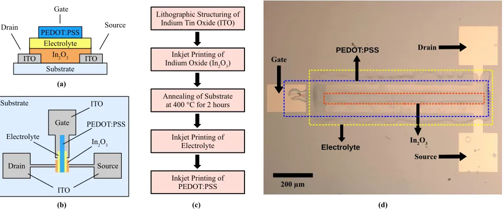
In the fabrication process of EGFETs, the channel material, indium oxide (In2O3) semiconductor, is inkjet printed to form
the channel between drain and source electrodes which use patterned indium tin oxide (ITO) as material. Then, on the top of the channel, the electrolyte is inkjet printed as gate dielectric. At last, PEDOT:PSS is inkjet printed on the top of the electrolyte as a top-gate in a way that it covers the channel area [22]. Figure 1 shows the structure, the fabrication process, and the photo of the EGFETs. As elaborated in Section III, patterned ITO electrodes (e.g., drain) can be used to align transistor images since it has less optically visible variation than printed inks (e.g., electrolyte) while the entropy of the proposed optical PUF are harvested from the optical image of printed inks of EGFETs.
B. Related Works
PUFs have become common in last decade to provide secret fingerprints [42]. They extract digital fingerprints from intrinsic manufacturing process variations. The inherent and uncontrollable variations ensure unpredictable fingerprints. Therefore, the fingerprints are utilized as a key for security purposes such as authentication and cryptography [17], [18], [49], [50], [51]. Several electrical PUFs have been proposed to secure integrated circuits and embedded systems. The most common electrical PUFs include SRAM PUF [52], Arbiter PUF [53], and Ring Oscillator PUF [54]. Furthermore, Printed memory PUF [55] and Printed Differential Circuit PUF [56] have been proposed in the context of PE.
On the other hand, recent research has also focused on optical PUFs for their advantages. Since Optical PUFs extracts randomness from optical variations, contrary to electrical PUFs, they require no additional circuitry in the product. Moreover, they provide high number of response bits. These advantages result in low-cost per piece, which make them beneficial for cost-limited applications [57], particularly for ultra-low-cost PE applications.
Lithographic Structuring of Indium Tin Oxide (ITO)
Inkjet Printing of Indium Oxide (In2O3)
Inkjet Printing of Electrolyte
Inkjet Printing of PEDOT:PSS Substrate
In2O3
ITO ITO
Electrolyte PEDOT:PSS
Drain Source
Gate
Gate
Drain Source
ITO
ITO
In2O3
PEDOT:PSS Electrolyte
Substrate Annealing of Substrateat 400 °C for 2 hours (a)
(b) (c)
Gate
Drain
Source
200 µm
In2O3
Electrolyte PEDOT:PSS
(d)
Figure 1: Description of Electrolyte-gated field effect transistor technology a) Cross-sectional view of EGFET on substrate [22]. b) Top view of EGFET on substrate [22]. c) Flow of fabrication process of EGFET [19]. d) Photo of a fabricated EGFET [19].
Camera
Region of Interest (ROI)
Fingerprint Extraction Methodology Challenge
Fingerprint 100111010011
Response
Figure 2: Overview of proposed optical PUF.
between pre-stored image and examined image after multiple processing steps, which requires large memory for pre-stored images resulting in high storage cost. For instance, the binary image size of a component is 1800x1800 corre-sponding to∼0.386 MB in the memory, and for high volume produced components, it increases proportionally (e.g., for 1 billion components, required memory is ∼368 TB), which harms its low-cost feature. The high memory usage of this method makes its utilization infeasible in ultra-low-cost PE applications. To the best of authors’ knowledge, our paper presents the first work extracting fingerprints from optically visible variations of PE inks with the objective of low memory usage in the literature.
III. PROPOSEDOPTICALPUF
The electrical PUFs introduce exorbitant overhead which is infeasible for ultra-low-cost PE applications. For instance, the electrical PUF proposed for PE in [55] containing three transistors and two resistors allocates∼3.5 mm2 generate one bit. Since the feature size of PE devices are large enough
A
lig
nm
en
t
Image
Normalization
Bilateral Denoising
Histogram Equalization
Adaptive Thresholding
Rotation
Template Matching
Fingerprint Compression
P
re
pr
oc
es
si
ng
Fingerprint
Figure 3: Proposed fingerprint extraction methodology com-posed of preprocessing, alignment, and fingerprint compres-sion.
(e.g., 10µm), one can capture the optically visible varia-tions of printed inks with a low-cost camera integrated to a microscope so that an optical PUF can extract multiple bits from one printed transistor, meaning that without any hardware overhead, multi-bit fingerprint can be generated. Therefore, the ultra-low-cost feature of PE has to be preserved while providing secure keys to prevent counterfeiting and overbuilding.
(a) (b)
(c) (d)
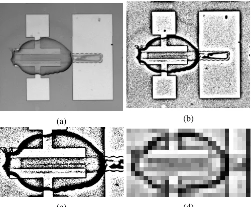
Figure 4: A printed transistor image (a) original, (b) prepro-cessed, (c) aligned (d) downscaled (downscaling factor=22).
unreliability are insufficient optical precision (different relative positioning), dust, camera noise and non-uniform illumination. We consider these challenges while developing the fingerprint extraction methodology of the proposed optical PUF.
The flow for extraction and processing of the proposed optical PUF is illustrated in Figure 2. It starts from the image acquisition using an optical camera integrated to a microscope, which is the challenge of the PUF. The preprocessing steps are applied to the acquired image to remove the effect of environmental conditions such as illumination and camera noise. After that, the images are aligned with respect to a reference. These steps are performed to ensure that the generated keys are reliably extracted. Last, to reduce the size of generated fingerprint, image downscaling is applied. The response of the PUF is the fingerprint consisting multiple bits. In the authentication phase, the extracted fingerprint of the examined printed component is compared with the fingerprints of all printed components which are stored in a secure data-center. The authentication of the printed component is verified based on the correlation of its fingerprint with a pre-stored fingerprint.
It should be noted that all steps described in this section are performed in pythonusing the scikit−image open source library [58]. The details of each step is elaborated in the following subsections.
A. Image Acquisition
The images are acquired by a camera integrated to a microscope. In each acquisition, an image with the dimension of 2560x1920 pixels, where four transistors fit, is taken since transistors fabricated to evaluate the methodology are close to each other on a substrate. Then, the image is divided into four images, each containing one transistor image with a size of ∼800x800. An example transistor image is shown in Figure 4a.
B. Preprocessing
To increase the reliability of the proposed optical PUF method with respect to noise and illumination differences, we apply the following preprocessing steps respectively:
• Normalization is used to scale the pixel values to the
range of [0,1] to reduce the effect of global lighting conditions, i.e. systematic shifts in the pixel value range.
• (Bilateral) Denoising[59] is an edge-preserving filtering.
While basic filters perform a weighted sum of close pix-els, bilateral filtering also considers their values. Through this, the pixels in the neighbourhood of a target pixel only have a strong influence if they also have a similar value before filtering. This is especially noticeable on sharp edges e.g. transitions from black to white. Here, black and white pixels would average to grey, where for bilateral filtering, the black pixels are not considered for white values (and vice versa) which leads to the preservation of the contrast after filtering.
• Histogram equalization [60] tries to achieve a more
equal distribution of the pixel value intensities in an im-age. For this, the images cumulative frequency histogram of the pixel values is used to transform the values of all pixels according to their rank in intensity. This leads to increased contrasts in the image while also decreasing the effect of global lighting conditions.
• Adaptive thresholdingbinarizes the image by comparing
the weighted neighbourhood of a pixel to a threshold value. If this threshold is exceeded, the pixel is declared black, else white is assigned.
The preprocessed version of the transistor image is shown in Figure 4b.
C. Alignment Correction
Following the preprocessing, the alignment of the images is applied to provide same relative positioning which increases the reliability of the fingerprint extraction with respect to shifts and rotations. For this purpose, first, a reference line, which is top edge of drain electrode (upper), is identified through a Hough Line Transform [61]. The images are then rotated such that the reference lines form the same angle to a horizontal line. Through this, an invariance to rotation is achieved. Then, a template matching [62] is performed on the rotated images to identify the position of the drain electrode, which will serve as a reference point to locate the region of the image containing electrolyte (region of interest i.e. ROI), which contains the most optically visible variation. The aligned version of the transistor image is given in Figure 4c, where the ROI is a 2-dimensional matrix containing bits, which then can be used as a fingerprint.
D. Fingerprint Compression
(a) (b)
(c) (d)
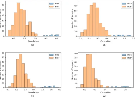
Figure 5: Intra and inter (pearson) correlation distribution of (a) Dataset-A, (b) Dataset-B, (c) Dataset-C, and (d) Dataset-D before downscaling (downscaling factor=1).
of 22 is depicted in Figure 4d. Moreover, the downscaling reduces the entropy of the image which results in worse uniquness (inter correlation), while on the contrary, mitigates the errors caused from misalignment, dust, camera noise and illumination differences which improves the reliability (intra correlation). This trade-off should be examined to optimize the downscaling factor.
IV. EVALUATIONRESULTS ANDDISCUSSIONS
In this section, we explain the metrics to evaluate the pro-posed optical PUF. Moreover, we describe the datasets which are used to validate the methodology. Finally, we report and discuss the results obtained using the proposed methodology applied to described datasets as well as security implications of the proposed PUF.
A. Evaluation Metrics
To quantify the quality of the proposed method, we use inter (uniqueness) and intra (reliability) correlation metrics. The uniqueness represents the correlation between the fingerprints of different EGFETs, and it should be low. The reliability represents the correlation between the fingerprints of same EGFET, and it should be high. Therefore, the fingerprints
of different EGFETs are distinguishable from the keys of same EGFETs with a threshold. It should be noted that, in this work, fast normalized cross-correlation [62] is used to calculate uniqueness and reliability.
The uniqueness of the optical PUF reflects the visible vari-ability of printed inks. The relivari-ability of the optical PUF suffers from misalignment, dust, camera noise, improper illumination and shape degradation over time.
The figure of merit (FoM) for the distinguishability is the difference between the minimum value of the reliability and the maximum value of the uniqueness, and is given by:
F oM(I) = min
{(i,j)|i=j, i,j∈I}C(i, j)−{(i,j)|maxi6=j, i,j∈I}C(i, j),
where the set I thereby denotes the multiset1 of all tran-sistor images. The first summand represents the intra cor-relation (reliability) between images of the same device i.e. i=j, i, j∈I, while the second summand denotes the inter correlation (uniqueness) between images of different devices i.e.i6=j, i, j∈I .
1The elements ofIare not unique since there are multiple imagesiof the
(a) (b)
(c) (d)
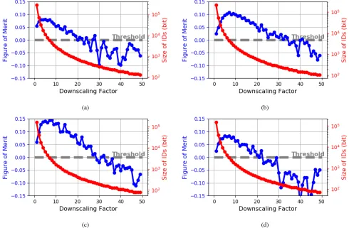
Figure 6: Figure of Merit (FoM) of (a) Dataset-A, (b) Dataset-B, (c) Dataset-C, and (d) Dataset-D with respect to downscaling factor (FoM: difference between minimum value of intra correlation and maximum value of inter correlation).
TABLE I: Definition of datasets
# of EGFETs
Width (µm)
Length (µm)
Size of ROI Image After Alignment
Dataset-A 18 600 60 350x780
Dataset-B 18 400 60 350x620
Dataset-C 18 200 60 350x460
Dataset-D 18 100 60 350x430
B. Dataset
We used the optical images of fabricated EGFETs to vali-date the methodology. The dataset is split into four subdataset, each containing EGFETs of a certain width (see Table I). Moreover, two images of each EGFET are taken with a time difference of 120 days to evaluate the reliability of the methodology in the context of camera noise, dust, illumination and the shape degradation over time.
C. Discussion of Results
The intra (reliability) and inter (uniqueness) correlation distributions of four datasets are given in Figure 5. The results show that with a certain threshold, the extracted fingerprints are distinguishable meaning that FoM is positive. The number of bits of the extracted fingerprints from A, dataset-B, dataset-C, and dataset-D are 273000, 217000, 161000, 150500-bit respectively. Please note that these number of bits
are achieved using only one printed transistor in the optical PUF while the printed electrical PUF provides 1-bit using 3 transistors and 2 resistors. To achieve the equal number (e.g., 150500) of bits using the electrical PUF, an area of∼0.5 m2is required, which is clearly infeasible. This comparison proves that the optical PUFs provides extremely larger number of bits with no hardware overhead and component cost.
since they start losing their distinctive features which leads to higher maximum inter correlation (worser reliability) and lower minimum intra correlation (worser uniqueness). There-fore, the fingerprints are less distinguishable while reaching better compression rates. The trade-off between distinguisha-bility and compression rate should be considered, and the downscaling rate should be selected according to targeted application specifications.
D. Discussion of Security Implications
As explained in Section I, the target of this work is to countermeasure counterfeiting and overbuilding of PE com-ponents. In most prominent attack scenarios, attacker has to clone the part of the component where optical PUF extracts the fingerprint so that the cloned component can be authenticated. Several cloning attacks have been performed on electrical PUFs [63], [64], [57]. However, such attacks have never been generalized on optical PUFs [57]. Therefore, more specific attack should be considered in the proposed optical PUF.
One possible attack is to use more precise subtractive tools (e.g. laser) than additive printing to clone the edge shape of ROI since ROI is the entropy source of the fingerprint. This can be achieved by either fabricating the component using subtractive methods or reshaping already printed inks. However, such costly fine-grained cloning attack has to be done in large volume to be economically viable for the attacker. However, using such costly precise processes defeats the purpose of ultra low-cost PE products, hence rendering such attack economically unfit. Furthermore, regardless of economical suitability, in both ways, attacker cannot imitate the thickness and smoothness of the edges (see Figure 4c) since the thickness and smoothness of ROI results from the random dispersion of inks, which is specific to additive manufacturing. Moreover, an additional step can be performed during the pre-processing to detect any sharp edges caused by subtractive processes directly.
E. Discussion of iPUF Usage in Supply Chain Tracking
In addition to the usage of iPUF in PE application for anti-counterfeting purpose, iPUF can be used for supply chain tracking thanks to its point-of-use fabrication feature. In the supply chain, each party can print a structure as a PUF (iP U Fi), which is a part of namely Super PUF along with
formerly printed structures (iP U F0, iP U F1, ..., iP U Fi−1).
When the end-user or any party in the chain receives the product, it has a Super PUF consisting of multiple iPUFs, printed by each previous party in the supply chain. This way, the chain can be uniquely tracked down.
The advantage of using iPUF in supply chain tracking is that it can be printed using low-cost tools (e.g., inkjet-printer), which results in ultra-low-cost overhead while providing suf-ficient resolution in the range of 10 µm, and intrinsic visual features to sustain the unclonability of the optical PUFs as discussed in Section IV-D.
V. CONCLUSION
The growing market of Printed Electronics (PE) bring about the counterfeiting of PE components. PUFs are commonly utilized to prevent the counterfeiting. However, electrical PUFs which require extra circuitry and associated overhead to prod-uct are infeasible in low-cost PE applications. In this paper, we present an image based fingerprint extraction methodology from the optical variation of printed inks in the PE com-ponents. Therefore, no extra circuitry is required to obtain such fingerprint. Moreover, we utilize an image downscaling to compress the extracted fingerprints to reduce the storage cost of the fingerprints. The methodology is applied to four datasets for evaluation. The results show that the optically visible variation of the printed inks are suitable to utilize in fingerprint extraction for anti-counterfeiting of PE, and the downscaling compression reduces the storage cost of the extracted fingerprints nearly 484x while maintaining adequate PUF metrics.
REFERENCES
[1] V. Subramanian, J. B. Chang, A. de la Fuente Vornbrock, D. C. Huang, L. Jagannathan, F. Liao, B. Mattis, S. Molesa, D. R. Redinger, D. Soltmanet al., “Printed electronics for low-cost electronic systems: Technology status and application development,” inESSCIRC 2008-34th European Solid-State Circuits Conference. IEEE, 2008, pp. 17–24. [2] D. Schaefer and W. M. Cheung, “Smart packaging: Opportunities and
challenges,”Procedia CIRP, vol. 72, pp. 1022–1027, 2018.
[3] P. Ferreira, R. Martinho, and D. Domingos, “Iot-aware business pro-cesses for logistics: limitations of current approaches,” in INForum, 2010, pp. 611–622.
[4] H. Mora, D. Gil, R. M. Terol, J. Azor´ın, and J. Szymanski, “An iot-based computational framework for healthcare monitoring in mobile environments,”Sensors, vol. 17, no. 10, p. 2302, 2017.
[5] G. Zhang, C. Li, Y. Zhang, C. Xing, and J. Yang, “Semanmedical: A kind of semantic medical monitoring system model based on the iot sensors,” in2012 IEEE 14th International Conference on e-Health Networking, Applications and Services (Healthcom). IEEE, 2012, pp. 238–243. [6] J. Marques, B. Pahl, and C. Kallmayer, “Thermoplastic packaging
and embedding technology for id-cards,” inMicroelectronics Packaging Conference (EMPC), 2013 European. IEEE, 2013, pp. 1–5. [7] L. W. F. Chaves and C. Decker, “A survey on organic smart labels for the
internet-of-things,” inNetworked Sensing Systems (INSS), 2010 Seventh International Conference on. IEEE, 2010, pp. 161–164.
[8] E. N. Mambou, S. Nlom, T. G. Swart, K. Ouahada, A. Ndjiongue, and H. C. Ferreira, “Monitoring of the medication distribution and the refrigeration temperature in a pharmacy based on internet of things (iot) technology,” in 2016 18th Mediterranean Electrotechnical Conference (MELECON). IEEE, 2016, pp. 1–5.
[9] F. Farabullini, F. Lucarelli, I. Palchetti, G. Marrazza, and M. Mascini, “Disposable electrochemical genosensor for the simultaneous analysis of different bacterial food contaminants,”Biosensors and Bioelectronics, vol. 22, no. 7, pp. 1544–1549, 2007.
[10] W. Burns, “Who launches taskforce to fight counterfeit drugs,”Bulletin of the World Health Organization, vol. 84, pp. 689–690, 2006. [11] H. Cheung and S. Choi, “Implementation issues in rfid-based
anti-counterfeiting systems,”Computers in Industry, vol. 62, no. 7, pp. 708– 718, 2011.
[12] S. A. S. Committeeet al., “Inquiry into counterfeit electronic parts in the department of defense supply chain,”Washington, DC: Author, 2012. [13] U. Guin, K. Huang, D. DiMase, J. M. Carulli, M. Tehranipoor, and
Y. Makris, “Counterfeit integrated circuits: A rising threat in the global semiconductor supply chain,”Proceedings of the IEEE, vol. 102, no. 8, pp. 1207–1228, 2014.
[15] J. S. Chang, A. F. Facchetti, and R. Reuss, “A circuits and systems perspective of organic/printed electronics: Review, challenges, and con-temporary and emerging design approaches,”IEEE Journal on Emerging and Selected Topics in Circuits and Systems, vol. 7, no. 1, pp. 7–26, 2017.
[16] A. T. Erozan, M. Hefenbrock, M. Beigl, J. Aghassi-Hagmann, and M. B. Tahoori, “Reverse engineering of printed electronics circuits: From imaging to netlist extraction,”IEEE Transactions on Information Forensics and Security, 2019.
[17] R. Pappu, B. Recht, J. Taylor, and N. Gershenfeld, “Physical one-way functions,”Science, vol. 297, no. 5589, pp. 2026–2030, 2002. [18] R. Maes and I. Verbauwhede, “Physically unclonable functions: A study
on the state of the art and future research directions,” in Towards Hardware-Intrinsic Security. Springer, 2010, pp. 3–37.
[19] A. T. Erozan, G. C. Marques, M. S. Golanbari, R. Bishnoi, S. Dehm, J. Aghassi-Hagmann, and M. B. Tahoori, “Inkjet-printed egfet-based physical unclonable function—design, evaluation, and fabrication,”
IEEE Transactions on Very Large Scale Integration (VLSI) Systems, vol. 26, no. 12, pp. 2935–2946, 2018.
[20] B. Wigger, T. Meissner, A. F¨orste, V. Jetter, and A. Zimmermann, “Using unique surface patterns of injection moulded plastic components as an image based physical unclonable function for secure component identification,”Scientific reports, vol. 8, no. 1, p. 4738, 2018. [21] V. Costa, A. Sousa, and A. Reis, “Cork as a unique object: Device,
method, and evaluation,”Applied Sciences, vol. 8, no. 11, p. 2150, 2018. [22] G. C. Marques, S. K. Garlapati, D. Chatterjee, S. Dehm, S. Dasgupta, J. Aghassi, and M. B. Tahoori, “Electrolyte-gated fets based on oxide semiconductors: Fabrication and modeling,”IEEE Transactions on Elec-tron Devices, vol. 64, no. 1, pp. 279–285, 2017.
[23] P. Rosa, A. Cˆamara, and C. Gouveia, “The potential of printed elec-tronics and personal fabrication in driving the internet of things,”Open Journal of Internet Of Things (OJIOT), vol. 1, no. 1, pp. 16–36, 2015. [24] C. Dagdeviren, B. D. Yang, Y. Su, P. L. Tran, P. Joe, E. Anderson, J. Xia, V. Doraiswamy, B. Dehdashti, X. Fenget al., “Conformal piezoelectric energy harvesting and storage from motions of the heart, lung, and diaphragm,”Proceedings of the National Academy of Sciences, vol. 111, no. 5, pp. 1927–1932, 2014.
[25] C. Steiger, A. Abramson, P. Nadeau, A. P. Chandrakasan, R. Langer, and G. Traverso, “Ingestible electronics for diagnostics and therapy,”Nature Reviews Materials, p. 1, 2018.
[26] Y. Chan, C. Kung, and Z. Pei, “Printed rfid: technology and applica-tion,” inRadio-Frequency Integration Technology: Integrated Circuits for Wideband Communication and Wireless Sensor Networks, 2005. Proceedings. 2005 IEEE International Workshop on. IEEE, 2005, pp. 139–141.
[27] V. Subramanian, P. C. Chang, D. Huang, J. B. Lee, S. E. Molesa, D. R. Redinger, and S. K. Volkman, “All-printed rfid tags: materials, devices, and circuit implications,” inVLSI Design, 2006. Held jointly with 5th International Conference on Embedded Systems and Design., 19th International Conference on. IEEE, 2006, pp. 6–pp.
[28] V. Subramanian, P. C. Chang, J. B. Lee, S. E. Molesa, and S. K. Volk-man, “Printed organic transistors for ultra-low-cost rfid applications,”
IEEE transactions on components and packaging technologies, vol. 28, no. 4, pp. 742–747, 2005.
[29] L. Yang and M. M. Tentzeris, “Design and characterization of novel paper-based inkjet-printed rfid and microwave structures for telecom-munication and sensing applications,” inMicrowave Symposium, 2007. IEEE/MTT-S International. IEEE, 2007, pp. 1633–1636.
[30] K. C. Honeychurch and J. P. Hart, “Screen-printed electrochemical sensors for monitoring metal pollutants,” TrAC Trends in Analytical Chemistry, vol. 22, no. 7, pp. 456–469, 2003.
[31] S. Laschi, I. Palchetti, and M. Mascini, “Gold-based screen-printed sensor for detection of trace lead,”Sensors and Actuators B: Chemical, vol. 114, no. 1, pp. 460–465, 2006.
[32] B. Li, S. Santhanam, L. Schultz, M. Jeffries-El, M. C. Iovu, G. Sauv´e, J. Cooper, R. Zhang, J. C. Revelli, A. G. Kusneet al., “Inkjet printed chemical sensor array based on polythiophene conductive polymers,”
Sensors and Actuators B: Chemical, vol. 123, no. 2, pp. 651–660, 2007. [33] F. C. Krebs, “Fabrication and processing of polymer solar cells: a review of printing and coating techniques,”Solar energy materials and solar cells, vol. 93, no. 4, pp. 394–412, 2009.
[34] R. Hahn and H. Reichl, “Batteries and power supplies for wearable and ubiquitous computing,” inWearable Computers, 1999. Digest of Papers. The Third International Symposium on. IEEE, 1999, pp. 168–169. [35] M. Hilder, B. Winther-Jensen, and N. Clark, “Paper-based, printed zinc–
air battery,”Journal of power Sources, vol. 194, no. 2, pp. 1135–1141, 2009.
[36] A. C. Arsenault, D. P. Puzzo, I. Manners, and G. A. Ozin, “Photonic-crystal full-colour displays,” Nature Photonics, vol. 1, no. 8, p. 468, 2007.
[37] J. Heikenfeld, P. Drzaic, J.-S. Yeo, and T. Koch, “A critical review of the present and future prospects for electronic paper,” Journal of the Society for Information Display, vol. 19, no. 2, pp. 129–156, 2011. [38] K. Flamm, “Measuring moore’s law: Evidence from price, cost, and
quality indexes,” National Bureau of Economic Research, Tech. Rep., 2018.
[39] V. Subramanian, J. B. Chang, A. de la Fuente Vornbrock, D. C. Huang, L. Jagannathan, F. Liao, B. Mattis, S. Molesa, D. R. Redinger, D. Soltmanet al., “Printed electronics for low-cost electronic systems: Technology status and application development,” inSolid-State Device Research Conference, 2008. ESSDERC 2008. 38th European. IEEE, 2008, pp. 17–24.
[40] C. D. Dimitrakopoulos and P. R. Malenfant, “Organic thin film transis-tors for large area electronics,”Advanced materials, vol. 14, no. 2, pp. 99–117, 2002.
[41] H. Sirringhaus, “25th anniversary article: Organic field-effect transistors: the path beyond amorphous silicon,”Advanced materials, vol. 26, no. 9, pp. 1319–1335, 2014.
[42] L.-L. Chua, J. Zaumseil, J.-F. Chang, E. C.-W. Ou, P. K.-H. Ho, H. Sirringhaus, and R. H. Friend, “General observation of n-type field-effect behaviour in organic semiconductors,”Nature, vol. 434, no. 7030, p. 194, 2005.
[43] S. Kyung, J. Kwon, Y.-H. Kim, and S. Jung, “Low-temperature, solution-processed, 3-d complementary organic fets on flexible substrate,”IEEE Transactions on Electron Devices, vol. 64, no. 5, pp. 1955–1959, 2017. [44] G. Cadilha Marques, D. Weller, A. T. Erozan, X. Feng, M. Tahoori, and J. Aghassi-Hagmann, “Progress report on “from printed electrolyte-gated metal-oxide devices to circuits”,”Advanced Materials, p. 1806483, 2019.
[45] S. K. Garlapati, N. Mishra, S. Dehm, R. Hahn, R. Kruk, H. Hahn, and S. Dasgupta, “Electrolyte-gated, high mobility inorganic oxide transis-tors from printed metal halides,”ACS applied materials & interfaces, vol. 5, no. 22, pp. 11 498–11 502, 2013.
[46] P. K. Nayak, M. N. Hedhili, D. Cha, and H. N. Alshareef, “High per-formance in2o3 thin film transistors using chemically derived aluminum oxide dielectric,”Applied Physics Letters, vol. 103, no. 3, p. 033518, 2013.
[47] A. T. Erozan, R. Bishnoi, J. Aghassi-Hagmann, and M. B. Tahoori, “Inkjet-printed true random number generator based on additive resistor tuning,” in2019 Design, Automation Test in Europe Conference Exhi-bition (DATE), 2019, pp. 1361–1366.
[48] Y. Qi, N. T. Jafferis, K. Lyons Jr, C. M. Lee, H. Ahmad, and M. C. McAlpine, “Piezoelectric ribbons printed onto rubber for flexible energy conversion,”Nano letters, vol. 10, no. 2, pp. 524–528, 2010. [49] M. Rostami, J. B. Wendt, M. Potkonjak, and F. Koushanfar, “Quo
vadis, puf?: trends and challenges of emerging physical-disorder based security,” in2014 Design, Automation & Test in Europe Conference & Exhibition (DATE). IEEE, 2014, pp. 1–6.
[50] M. Rostami, F. Koushanfar, and R. Karri, “A primer on hardware security: Models, methods, and metrics,”Proceedings of the IEEE, vol. 102, no. 8, pp. 1283–1295, 2014.
[51] C. Herder, M.-D. Yu, F. Koushanfar, and S. Devadas, “Physical unclon-able functions and applications: A tutorial,”Proceedings of the IEEE, vol. 102, no. 8, pp. 1126–1141, 2014.
[52] D. E. Holcomb, W. P. Burleson, and K. Fu, “Power-up sram state as an identifying fingerprint and source of true random numbers,” IEEE Transactions on Computers, vol. 58, no. 9, pp. 1198–1210, 2008. [53] B. Gassend, D. Clarke, M. Van Dijk, and S. Devadas, “Silicon physical
random functions,” in Proceedings of the 9th ACM conference on Computer and communications security. ACM, 2002, pp. 148–160. [54] G. E. Suh and S. Devadas, “Physical unclonable functions for device
authentication and secret key generation,” in 2007 44th ACM/IEEE Design Automation Conference. IEEE, 2007, pp. 9–14.
[55] A. T. Erozan, G. C. Marques, M. S. Golanbari, R. Bishnoi, S. Dehm, J. Aghassi-Hagmann, and M. B. Tahoori, “Inkjet-printed egfet-based physical unclonable function—design, evaluation, and fabrication,”
IEEE Transactions on Very Large Scale Integration (VLSI) Systems, vol. 26, no. 12, pp. 2935–2946, 2018.
[57] U. R¨uhrmair, C. Hilgers, S. Urban, A. Weiersh¨auser, E. Dinter, B. Forster, and C. Jirauschek, “Optical pufs reloaded,”Eprint. Iacr. Org, 2013.
[58] S. van der Walt, J. L. Sch¨onberger, J. Nunez-Iglesias, F. Boulogne, J. D. Warner, N. Yager, E. Gouillart, T. Yu, and the scikit-image contributors, “scikit-image: image processing in Python,”PeerJ, vol. 2, p. e453, 6 2014. [Online]. Available: http://dx.doi.org/10.7717/peerj.453 [59] C. Tomasi and R. Manduchi, “Bilateral filtering for gray and color images,” inComputer Vision, 1998. Sixth International Conference on. IEEE, 1998, pp. 839–846.
[60] S. M. Pizer, E. P. Amburn, J. D. Austin, R. Cromartie, A. Geselowitz, T. Greer, B. ter Haar Romeny, J. B. Zimmerman, and K. Zuiderveld, “Adaptive histogram equalization and its variations,”Computer vision, graphics, and image processing, vol. 39, no. 3, pp. 355–368, 1987. [61] R. O. Duda and P. E. Hart, “Use of the hough transformation to detect
lines and curves in pictures,”Communications, 1972.
[62] U. D. H. Kai Briechle, “Template matching using fast normalized cross correlation,” 2001. [Online]. Available: https://doi.org/10.1117/12.421129