Volume 4, No. 9, July-August 2013
International Journal of Advanced Research in Computer Science
RESEARCH PAPER
Available Online at www.ijarcs.info
ISSN No. 0976-5697
VLSI Implementation of Neural Network for Signal Compression & Decompression
S.R.Kshirsagar
Electronics engineering & telecommunication department G.H.Raisoni college of engg. & management
Amravati, India [email protected]
Prof. A.O.Vyas
Electronics engineering & telecommunication department G.H.Raisoni college of engg. & management
Amravati, India [email protected]
Prof. A.D.Raut
Electronics engineering department Dr. Rajendra Gode Polytechnic college
Amravati, India [email protected]
Abstract: Artificial intelligence is realized based on mathematical equations and artificial neurons. In the proposed design, our main focus is on the implementation of chip layout design for Feed Forward Neural Network Architecture (NNA) in VLSI for generic analog signal processing applications. The analog components like Gilbert Cell Multiplier (GCM), Adders, Neuron activation Function (NAF) are used in the implementation. This neural architecture is trained using Back propagation (BP) algorithm in analog domain with new techniques of weight storage.
We are using 45nm CMOS technology for layout designing and verification of proposed neural network. The functionality of proposed design of neural network will be verified for analog operations like signal amplification and frequency multiplication.
Keywords: Gilbert cell, neuron activation function, neural network, VLSI, signal compression, signal decompression.
I. INTRODAUCTION
Intelligence is the computational part of the ability to achieve goals in the world. This intelligence though a biological word is realized based on the mathematical equations, giving rise to the science of Artificial Intelligence(AI). To implement this intelligence artificial neurons are used.
These artificial neurons comprised of several analog components. The neuron selected is comprises of multiplier and adder along with the tan-sigmoid function. The training algorithm used is performed in analog domain thus the whole neural architecture is analog structure. The proposed technology is a step in the implementation of neural network architecture using back propagation algorithm. These artificial neurons, we are realizing by Analog components like multipliers, adders and differentiators. The electronic industry has achieved a phenomenal growth over last two decades, mainly due to rapid advances in integration technologies, large scale systems design – in short, due to the advent of VLSI technology. The number of applications of integrated circuits in high performance computing, telecommunications, and consumer has been rising steadily, and at a very fast pace [1].
Mainly due to the rapid advances in integration technologies, large-scale systems design - in short, due to the advent of VLSI Technology. The number of applications of integrated circuits in high-performance computing, telecommunications, and consumer electronics has been rising steadily, and at a very fast pace. Typically, the required computational power (or, in other words, the intelligence) of
these applications is the driving force for the fast development of this field.
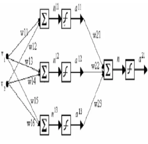
Figure 1: layered neural network
generated by adder blocks is given to the Neuron Activation function [2]. The output of activation function is multiplied by weights again and given to the input blocks of output layer.This layered structure of neural network is implemented in VLSI using analog components. Gilbert cell multiplier, adder and differential amplifier are used for different blocks.
II. RESULTSANDDISCUSSION
A. Gilbert cell:
The Gilbert cell is used as the multiplier block [3]. The main building blocks of Gilbert cell are differential pair transistors, current mirror circuit.
The schematic diagram, layout structure and simulation of the Gilbert cell is as shown below.
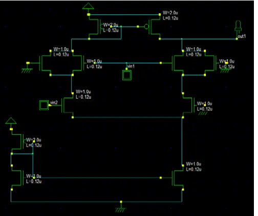
B. Schematic of gilbert cell:
Figure 2 shows the schematic of gilbert cell which is designed using DSCH3.1 tool.
Figure 2: Schematic of gilbert cell
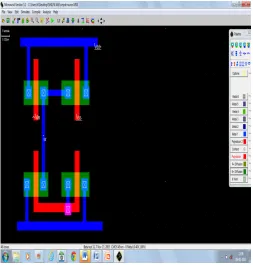
C. Layout of gilbert cell:
The following figure 3 shows the layout of gilbert cell which is designed using, 45nm VLSI technology & it is the first block of proposed design.
Figure 3: layout of Gilbert cell
D. Simulation of Gilbert Cell:
Figure 4 shows the voltage versus time response of gilbert cell.
Figure 4: Voltage versus time response of gilbert cell Neuron activation function
Validation is a critical aspect of any model construction. Although, there does not exist as well formulated or theoretical methodology for neural network model validation, the usual Practice is to base model validation upon some specified network performance measure of data that was not used in model construction (a “test set”)[4]. In this neural network we are using neuron activation function for validation. It will compare the input signal with the reference signal and then output will be generated.
Neurons use sigmoidal type activation functions. Sigmoidal type functions allow simple networks the ability to describe complex surfaces. Nonlinear activation functions of neurons are essential for neural network operation. Such sigmoidal functions can be created in the differential pair [2].
E. Schematic of neuron activation function:
Figure 5 shows the schematic of neuron activation function which is designed using DSCH3.1 tool.
Figure 5: schematic of neuron activation function
F. Layout of neuron activation function:
Following figure shows the layout of neuron activation function which is designed using microwind3.1 software, 45nm CMOS technology.
Figure 6: layout of neuron activation function
G. Simulation of neuron activation function:
Following figure 7 shows the voltage versus time response of neuron activation function.
Figure 7: Voltage versus time response of neuron activation function
H. Neural network for signal compression:
a. Schematic of neural network for signal
compression:
Figure 8 shows the schematic of neural network for signal compression. Here two analog signals are given as inputs and single signal is obtained at the output which is compressed signal [5].
Figure 8: Schematic of neural network
Figure 9 shows the layout of neural network for signal compression.
Figure 9: layout of neural network for signal compression
J. Simulation of neural network for signal
compression:
Figure 10 shows the voltage versus time response of neural network for signal compression.
Figure 10: Voltage versus time response of neural network for signal compression
K. Neural network for signal compression
a. Schematic of neural network for signal
decompression:
Figure 11 shows the schematic of neural network for signal decompression. Here single analog signal is given as input, which is output generated by neural network for signal compression. Two output signals are produced which are same as inputs given to the neural network for signal decompression.
Figure 11: Schematic of neural network for signal decompression
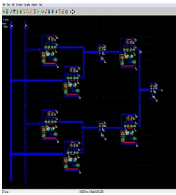
L. Layout of neural network for signal decompression:
The following figure 12 shows the layout of neural network for signal decompression which is designed using microwind 3.1 software in 45nm CMOS technology.
M. Simulation of neural network for signal decompression:
Figure13: Voltage versus time response of neural network for signal decompression
III. CONCLUSION
VLSI technology is the fastest growing field today. Considering the advancement of future technology and the advantage of 45 nm technology over 65 and 90 nm
technology, the selection of 45nm technology for the proposed project was the proper choice of technology.
The VLSI implementation of a feed forward neural network for analog signal processing has been demonstrated in this project. To give an application oriented approach two analog signals are compressed and decompressed using the designed feed forward neural network and the simulation results are obtained in 45nm CMOS VLSI technology.
IV. REFERENCES
[1] Jun Zhao, Yong –Bin Kim"A Low-Power Digitally Controlled Oscillator for All Digital Phase-Locked Loops" VLSI Design Volume 2010
[2] B. M. Wilamowski, J. Binfet, and M. O. Kaynak “VLSI Implementation of Neural Networks”
[3] Gilbert Multiplier by Ari Sharon, aris@cs, Ariel Zentner , relz@cs, ZachiSharvit, zachi@cs, Yaakov Goldberg, yaakov@cs
[4] Rafid Ahmed Khalil &Sa'ad Ahmed Al-Kazzaz “Digital Hardware Implementation of Artificial Neurons Models UsingFPGA”pp.12-24
[5] NeerajChasta, SaritaChouhan and Yogesh Kumar “Analog VLSI Implementation of Neural Network Architecture for Signal Processing”VLSICS April 2012