ABSTRACT
WANG, WEIHU. Systematic Optimization of Phase Noise of Voltage-Controlled Oscillators for Millimeter-Wave Radar. (Under the direction of Brian Floyd.)
Silicon technology has advanced to the point that millimeter-wave transceiver systems operating
up to 100 GHz can be integrated to realize sophisticated functionality at reduced consumer cost.
These millimeter-wave radar and radio systems require a high-performance local oscillator (LO)
solution to generate reference signals used within the receiver and transmitter. As a consequence,
novel design techniques for voltage-controlled oscillators (VCOs) in the millimeter-wave frequency
range are needed to achieve low phase noise, wide tuning range, and low energy consumption.
Although integrated VCOs have been studied for decades, challenges also emerge as the operating
frequency goes up, with the passive device quality (Q) factor and the transistor speed becoming two
limiting factors that degrade performance.
First, VCOs used in frequency-modulated continuous-wave (FMCW) radar applications require
wide continuous tuning range and low phase noise simultaneously. These high-gain VCOs will
typically have high phase noise, due to a high conversion from amplitude-modulated noise to
phase-modulated noise arising in the VCO’s tuning path and the bias circuitry. A transformer-coupled
inductor-capacitor (LC) tank is introduced which can enable wide tuning-range and low phase noise
simultaneously, suitable for both long-range and short-range FMCW radar sensors. To demonstrate
the technique, a 20GHz VCO with wide continuous tuning range is incorporated in a W-band FMCW
radar transceiver (TRX). The VCO satisfies both the phase noise requirement of long-range radar
(LRR) and the tuning range requirement of short-range radar (SRR), effectively reducing the area
and cost of an otherwise two VCO solution.
Second, the active circuit affects phase noise through the additional noise being injected into
the tank as well as the signal power of oscillation, whereas power efficiency of the active device
is also crucial for certain applications. In this study, these problems are addressed using a newly
proposed ring-type LC quadrature VCO (QVCO), which, when compared to a conventional Colpitts
structure, has a smaller loading capacitance to the LC tank. To demonstrate the usefulness of this
topology, a 20 GHz QVCO is fabricated in conjunction with a frequency quadrupler as a solution to
communication systems.
Third, as suggested by Leeson’s equation, the passive Q has a significant impact on phase noise.
To handle the passive device Q factor, the loss mechanism and accurate modeling of monolithic
inductors have been studied thoroughly in the literature; however, despite the accurate modeling,
designers still often approach the optimization problem on a trial-and-error basis. Hence, it is of
interest to study the impact of operating frequency on passive Q, thus clarifying the choice of the
VCO operating frequency. In this work, a systematic study will be presented on the optimization
and frequency response of resonator Q. Based on the result, it is made possible to predict the phase
noise before actually designing the circuit, given the operating frequency, tuning range, and power
requirement of the VCO. This then provides a method which system designers can use for deciding
the best VCO frequency. To demonstrate the validity of this approach, VCOs are simulated and
measured at 10 GHz, 20 GHz, and 40 GHz for comparison.
As will be shown in this dissertation, the systematic optimization of millimeter-wave VCO
consists of technology analysis and performance prediction techniques in the aspects of passive
© Copyright 2018 by Weihu Wang
Systematic Optimization of Phase Noise of Voltage-Controlled Oscillators for Millimeter-Wave Radar
by Weihu Wang
A dissertation submitted to the Graduate Faculty of North Carolina State University
in partial fulfillment of the requirements for the Degree of
Doctor of Philosophy
Electrical Engineering
Raleigh, North Carolina
2018
APPROVED BY:
Paul Franzon Rhett Davis
Zhilin Li Brian Floyd
DEDICATION
BIOGRAPHY
Weihu Wang received the B.E. degree in electronics and communication engineering from China
Uni-versity of Petroleum, Beijing, China, in 2010. He received the M.Sc. degree in electrical engineering
from North Carolina State University, Raleigh, USA, in 2012.
In 2012, Weihu joined the iNtegrated Circuits and Systems lab at NC State under the direction of
Prof. Brian Floyd. His research focuses on analog and RF integrated circuits, particularly monolithic
ACKNOWLEDGEMENTS
First of all, I would like to thank my advisor, Prof. Brian Floyd, for his persistent guidance and
support. Prof. Floyd not only supplied me with knowledge and ideas, but also lead as a role model
of a professional researcher. I would also like to thank Prof. Paul Franzon, Prof. Rhett Davis, and
Prof. Zhilin Li, for serving on my dissertation committee with their expertise.
I would like to express my gratitude to managers and engineers from Asahi Kasei Microdevices
Corporation for their partnership, especially T. Fujibayashi, Y. Takeda, K. Kishigami, and S. Takeuchi.
My gratitude also goes to N. Cahoon from GlobalFoundries for donating chip area for experimental
studies. I would like to thank Prof. P. Franzon on my committee who is also from the Center for
Advanced Electronics through Machine Learning (CAEML), along with students Weiyi Qi and Yi
Wang from the center, for collaboration on circuit design. I would also like to thank Prof. M. Steer,
Prof. D. Ricketts, Dr. S. Lipa, and Dr. M. Abbasi, for their help and instructions.
I am also grateful for the suggestions and discussions offered by students and friends from
my research lab and neighboring labs in the Monteith Engineering Research Center. These people
include Yi-Shin Yeh, Kevin Greene, Anirban Sarkar, Vikas Chauhan, Charley Wilson, Jeff
Bonner-Stewart, Sandeep Hari, Xiao Xiang, Deeksha Lal, Junyu Shen, and Xiaopeng Duan. Last, I would like
TABLE OF CONTENTS
LIST OF TABLES . . . vii
LIST OF FIGURES. . . .viii
Chapter 1 Introduction. . . 1
1.1 Millimeter-Wave Radar Sensors . . . 2
1.2 Local Oscillator Phase Noise . . . 7
1.3 Research Objectives . . . 11
Chapter 2 Millimeter-Wave VCO Techniques . . . 14
2.1 VCO Performance Specifications . . . 15
2.2 The LC Tank . . . 16
2.3 Types of VCO Topology . . . 20
2.4 Theoretical Phase Noise Studies . . . 22
Chapter 3 Split-Inductor Tunable Resonator. . . 24
3.1 Requirement of FMCW Generator . . . 25
3.2 Characteristics of Split-Inductor Tunable Resonator . . . 27
3.2.1 Noise Benefits with Transformer Resonator . . . 27
3.2.2 Impact of Capacitive Coupling . . . 29
3.2.3 Impact of Magnetic Coupling . . . 33
3.2.4 Impact of Substrate Coupling . . . 38
3.3 VCO Implementation . . . 40
3.3.1 Transformer Considerations . . . 41
3.3.2 VCO Colpitts Core . . . 43
3.3.3 Integration into FMCW Transceiver . . . 46
3.4 Measurement Results . . . 48
3.5 Conclusions . . . 51
Chapter 4 Ring-Type LC Quadrature Active Topology . . . 54
4.1 Requirement of Active Device . . . 55
4.2 Characteristics of Ring-Type LC Quadrature VCO . . . 57
4.2.1 Transconductance of Capacitive Injection . . . 58
4.2.2 Phase Noise Analysis . . . 61
4.2.3 Large-Signal Phase Noise Expressions . . . 66
4.3 VCO Implementation . . . 68
4.3.1 Transformer . . . 69
4.3.2 Varactors and Oscillation Amplitude Equalization . . . 71
4.3.3 Transistors and the Feedback Capacitor Network . . . 78
4.3.4 The Adjustable Biasing Network . . . 79
4.4 Measurement Result . . . 79
4.5 Conclusions . . . 83
Chapter 5 Systematic Optimization of VCO Phase Noise . . . 85
5.1 Optimization Goals . . . 86
5.2.1 Quality Factor of Inductors . . . 90
5.2.2 Peak Inductor Q Explanation . . . 92
5.3 Varactor Optimization . . . 98
5.4 Noise Modulation of Active Device . . . 101
5.4.1 Circuit Topology Versus Operating Frequency . . . 102
5.4.2 Circuit Topology Versus Transistor Characteristics . . . 104
5.4.3 Comparison of Common Types of VCO Topology . . . 106
5.5 Phase Noise Estimation Procedure . . . 108
5.6 VCO Implementation . . . 112
5.6.1 Unified VCO Topology for Three Different Frequencies . . . 114
5.6.2 VCO Buffer Using Wide-Band Emitter Follower . . . 119
5.7 Measurement Result . . . 119
5.8 Conclusions . . . 122
Chapter 6 Conclusions . . . .125
6.1 Technical Contributions . . . 125
6.2 Future Work . . . 126
LIST OF TABLES
Table 3.1 Comparison with State-of-the-art Wide Tuning-range VCOs . . . 52
Table 4.1 Comparison of existing QVCO techniques in the literature . . . 56 Table 4.2 Comparison of Noise Parameters and Phase Noise Readings under Various
Circuit Conditions for the QVCO . . . 68
LIST OF FIGURES
Figure 1.1 Example of the transmitted signal of a FMCW radar. . . 3 Figure 1.2 Illustration of the received signal in the presence of transmitter phase noise. 5 Figure 1.3 Simplified radar transceiver architecture. . . 6 Figure 1.4 Sketch of the SSB phase noise of a free-running VCO. . . 8 Figure 1.5 Sketch of the SSB phase noise of a PLL output. . . 10 Figure 1.6 Overview of the approaches to the systematic optimization of
millimeter-wave VCOs. . . 12
Figure 2.1 Schematic of a simple cross-coupled VCO with external biasing. . . 20 Figure 2.2 Schematic of two variants of a Colpitts VCO: the common-collector variant
(left) and the common-base variant (right). . . 21
Figure 3.1 Simplified schematics of the AC-coupled varactor (left) versus the split-inductor tunable resonator (right) used within differential Colpitts VCO. . . 26 Figure 3.2 The phase noise degradation in dB due to choke resistors at select circuit
conditions. . . 28 Figure 3.3 Topology of the simplified fourth-order resonator with capacitive coupling:
extracted half-circuit. . . 29 Figure 3.4 Topology of the simplified fourth-order resonator with capacitive coupling:
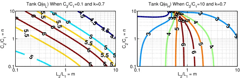
half-circuit with loss for impedance analysis. . . 29 Figure 3.5 Tank Q analyzed at the lower resonant frequency when C3/C1=0.1 (left).
Tank Q analyzed at the higher resonant frequency when C3/C1=0.1 (right). . 31 Figure 3.6 Tank Q analyzed at the lower resonant frequency when C3/C1=10 (left). Tank
Q analyzed at the higher resonant frequency when C3/C1=10 (right). . . 32 Figure 3.7 Tank Q at the lower resonant frequency with small C3/C1=0.1 and k=0.7
(left). Tank Q at the higher resonant frequency with large C3/C1=10 and k=0.7 (right). . . 32 Figure 3.8 The skeptical coupling model of transformer windings. . . 34 Figure 3.9 The concentric traces used in EM simulation. . . 34 Figure 3.10 The transformer windings in individual metal levels used in EM simulation
for the concentric trace study. . . 35 Figure 3.11 Parallel connection of transformer with loss resistance for equivalent impedance
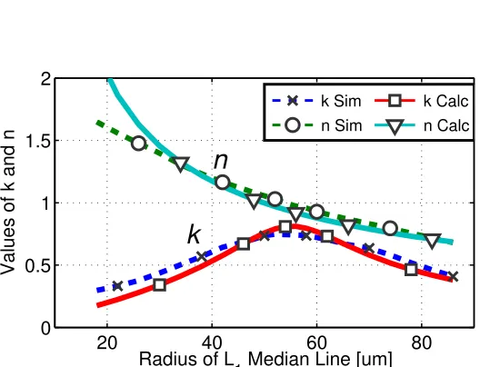
analysis. . . 35 Figure 3.12 EM-extracted and calculated coupling factor (k) and turns ratio (n).L2radius
fixed at 55µm, whileL1radius is varied from 18 to 84µm.L1width is 20µm, andL2width is 28µm. . . 36
Figure 3.13 EM-extracted and calculated inductance values for the same group of trans-formers (left). EM-extracted and calculated series resistance of the AC-shorted windings considering proximity effect for the same group of transformers (right). . . 37 Figure 3.14 Extraction model for inductor considering metal and substrate loss, showing
originalπ-model. . . 38 Figure 3.15 Extraction model for inductor considering metal and substrate loss, showing
Figure 3.16 X/2pif and X/R of inductor impedance to show accuracy of data-fit. (left) Se-ries resistance (real part) of the inductor impedance showing decomposition of loss into metal and substrate. (right) . . . 39 Figure 3.17 EM-simulated Q of a “split-inductor” with windings having the same pattern
vertically aligned versus Q of a single inductor. . . 40 Figure 3.18 Example layout of the “split-inductor”.L1is on top-level metal;L2is on next
highest level of metal. A ground shield is used for the structure. . . 41 Figure 3.19 EM-simulated inductance and Q of the AC-shorted transformer traces used
in the tank. The transformer has n=1.25 and k=0.4. (left) Small-signal model and simulated impedance of the transformer-coupled tank versus frequency. (right) . . . 42 Figure 3.20 Block diagram of the VCO core and auxiliary circuit for the FMCW radar
transceiver. . . 43 Figure 3.21 Schematic of the complete VCO core circuit. . . 45 Figure 3.22 Schematic of VCO buffer and frequency doubler. . . 47 Figure 3.23 Die micrograph of the VCO, buffer, first frequency doubler, and divide-by-4
prescaler, all of which are integrated into a radar transceiver. . . 48 Figure 3.24 Measured VCO tuning curves, with required range for both LRR and SRR
modes indicated with dark and light shaded boxes, respectively (left). Mea-sured VCO tuning gain for LRR and SRR modes across temperature (right).
. . . 49 Figure 3.25 Single-sideband phase noise @1MHz offset measured at the output of the
divide-by-four circuit across tuning range at 25°C (left). Single-sideband phase noise @1MHz offset measured at both the transmitter PA chain and the divide-by-four circuit for short-range radar mode at 25°C with RDAC=40 (right). . . . 49 Figure 3.26 Measured VCO phase noise @1MHz offset of divider output at optimum bias
settings in SRR and LRR modes, for 25 °C (RDAC=40) and 125 °C (RDAC=60). 50 Figure 3.27 Measured phase noise @1MHz offset of divider output across band in SRR
mode as function of RDAC setting at 25°C. . . 51
Figure 4.1 Concept of the proposed ring-type quadrature VCO using capacitive coupling. 57 Figure 4.2 Half-circuit of two variants of conventional Colpitts structures. . . 59 Figure 4.3 Simplified diagram of the proposed mobius LC VCO. . . 60 Figure 4.4 Comparison of the proposed mobius LC topology to conventional Colpitts in
terms of their negative transconductanceRe[Ym]/gmand fixed tank loading Im[Ym]/gm. . . 61 Figure 4.5 Schematic of a single branch for deriving the large-signal expressions. . . 63 Figure 4.6 Comparison of the simulated and calculated tank voltage and current
wave-forms. . . 65 Figure 4.7 Complete schematic of the ring-type LC quadrature VCO including control
circuitry. . . 70 Figure 4.8 Schematic of the varactor banks showing tank resistance equalization. . . 72 Figure 4.9 Simulation of oscillation amplitude and phase noise using the single DGNCAP
varactor and showing estimated optimum values. . . 73 Figure 4.10 Schematic of the varactor banks showing tank resistance equalization. . . 73 Figure 4.11 Comparison of oscillation amplitude and frequency across tuning range using
Figure 4.12 Spot phase noise across tuning range and varactor transient voltage waveform using the single DGNCAP varactor and equalized varactor banks. . . 75 Figure 4.13 The transient voltage waveform using (a) a series connection of three NCAP
(left), and (b) an engineered series connection of two NCAP and one resistor (right) to equalize oscillation amplitude. . . 76 Figure 4.14 Schematic of the tank with three series NCAP for amplitude equalization. . . 76 Figure 4.15 Schematic of the tank with an engineered series network of two NCAP and
one resistor for amplitude equalization. . . 77 Figure 4.16 The oscillation amplitude variation across tuning range (left) and phase noise
at 10 MHz offset variation across tuning range (right) for the tank structure with an engineered series connection of two NCAP and one resistor to equalize oscillation amplitude. . . 77 Figure 4.17 Layout of the active device, the coupling capacitors, and the interconnects. . 78 Figure 4.18 Layout of the active device, the coupling capacitors, and the interconnects. . 79 Figure 4.19 Good agreement between simulation and measurement results for tuning
range (upper-left) and phase noise at various bias current. . . 80 Figure 4.20 Complete schematic of the ring-type LC quadrature VCO including control
circuitry. . . 81 Figure 4.21 Oscillation amplitude in various bias current settings (left), and Measured
phase noise at the 10 MHz offset (right). . . 81 Figure 4.22 The frequency sensitivity with respect to tuning voltage and oscillation
am-plitude. . . 82 Figure 4.23 The chip micrograph including VCO, pre-amplifier, and quadrupler. . . 83
Figure 5.1 Several options to generate a 80 GHz LO signal. . . 87 Figure 5.2 EM simulation results of a group of inductors with various radii and width.
The inductor widths take values of 10, 15, 20, 25, 30, 35, 40, 50, 60, and 80µm; whereas, the total lengths take values of 50, 75, 100, 125, 150, 200, and 250 µm. Data are interpolated in between the samples to draw contours. . . 91 Figure 5.3 Schematic of the inductor π-model including parasitic and loss used for
frequency analysis. . . 92 Figure 5.4 Simplified inductor model using equivalent parallel parasitic and loss for
peak Q exploration. . . 95 Figure 5.5 Comparison of best geometry calculation and EM simulation of a group of
inductors with various radii and width. The red dotted line represents the calculated geometry(w l)o p t for each frequency. The circle-cross marker represents the chosen optimum width and length for best inductor Q. The same group of simulation data as Fig. 5.2 are used and drawn in black and white. . . 96 Figure 5.6 Tank capacitance modeled as a parallel connection of varactor and fixed
capacitance. . . 99 Figure 5.7 Comparison of select sizes of thin and thick gate-oxide MOSCAP using
Figure 5.9 Chip micro-graph of the 20 GHz (top half ) and 40 GHz (bottom half ) opti-mized VCO. . . 113 Figure 5.10 Top-level schematic of the 10, 20, and 40 GHz optimized VCO. . . 114 Figure 5.11 Detailed schematic of the LC tank (left) and tail current source (right) of the
unified QVCO topology for 10, 20, and 40 GHz VCO. . . 115 Figure 5.12 Layout overview of the 10 GHz VCO. . . 117 Figure 5.13 The closed-in view of the capacitors and transistors layout close to the center
showing details of the higher-level metal and devices (left) and lower-level metals and devices (right) of the 10 GHz VCO. . . 118 Figure 5.14 VCO buffer implemented as a wide-band emitter follower 10, 20, and 40 GHz
VCO. . . 118 Figure 5.15 Frequency (left) and phase noise @ 1MHz offset (right) of the optimized 10
GHz VCO. . . 119 Figure 5.16 Output power level (left) and phase noise @ 10MHz offset (right) of the
opti-mized 10 GHz VCO. . . 120 Figure 5.17 Frequency (left) and phase noise (right) of the optimized 20 GHz VCO. . . 120 Figure 5.18 Output power level (left) and phase noise @ 10MHz offset (right) of the
opti-mized 20 GHz VCO. . . 121 Figure 5.19 Frequency (left) and phase noise (right) of the optimized 40 GHz VCO. . . 121 Figure 5.20 Output power level (left) and phase noise @ 10MHz offset (right) of the
CHAPTER
1
INTRODUCTION
The innovation of nano-fabrication has supplied a sustained growth of affordable electronics with
faster transistors. As the available spectrum in the millimeter-wave frequency is explored, more
applications have drawn the interests of the industry and academia alike. The most popular ones
among these emerging applications include 57-64 GHz and 64-71 GHz wireless gigabit
communica-tions, 76-81 GHz vehicular radar, and 71-76 GHz, 81-86 GHz, and 92-95 GHz point-to-point and
satellite communication. For example, radars were once implemented as bulky discrete
compo-nents, but with today’s advanced fabrication in both complementary metal-oxide semiconductor
(CMOS) and bipolar technologies, integrated solutions have become popular. Researches have
recently focused on enabling large-scale integration of high-performance millimeter-wave systems,
as well as providing advanced digital control and on-chip built-in-self-test (BIST) functions.
The primary driver is, of course, cost reduction of these solutions through mass production.
Integration also enables increased portability, improved performance, and energy savings. As the
silicon technology changes, circuit techniques must adapt and leverage the performance benefits
makes advanced millimeter-wave circuit design an area of active research. A better understanding
of the dependency between technology and circuit performance ensures that a circuit can be fully
optimized, thus is greatly appreciated in both the academia and industry. In this study, a key part of
the effort is to reveal the dependency between technology and circuit for millimeter-wave
voltage-controlled oscillators (VCOs), which is one layer of investigation in advanced of the related works
on application-driven technique improvement.
1.1
Millimeter-Wave Radar Sensors
In this study, radar transceivers is emphasized as the target market. Radar solutions have existed
for decades in the automotive and industrial fields. In the automotive field, the various
applica-tions can be generally categorized into short-range radar and long-range radar. The short-range
radar applications include blind-spot detection, lane-change assistance, and the long-range radar
applications include emergency braking, and autonomous cruise control. In the industrial field,
millimeter-wave radars are commonly used for fluid level detection, material detection, and radio
astronomy.
Millimeter-wave radars have been implemented in 24 GHz and 60 GHz unlicensed industrial,
scientific, and medical (ISM) bands, which are considered as narrow-band. They are recently
imple-mented in 76-77 and 77-81 GHz, which opens up opportunities for many applications due to its
ultra-wide bandwidth allocation. The wide bandwidth available at 79 GHz can be used to improve
range resolution, which results in better separation of closely located targets that are susceptible to
aliasing. This allows the radar to detect a small object in the vicinity of a larger one, e.g. a person
beside a car, and is useful for sophisticated vehicular control in short-range radar applications. The
design of this feature in a frequency-modulated continuous-wave (FMCW) radar follows the physics
that the range resolution is inversely proportional to sweep bandwidth and is irrelevant to sweep
time. The velocity resolution can also benefit from sweep bandwidth, and this is especially useful
for accurate detection of slowly moving targets.
As newer technology is introduced, challenges also emerge when millimeter-wave radars further
evolve into self-driving vehicles. One of such challenges comes from the limitation in the resolution
detection or false alarms, which is a safety risk. Another challenge comes from the influence of the
atmosphere either due to adverse weather, which alters the electrical properties of the medium for
wave propagation, or due to interference from nearby millimeter-wave emissions. This requires
advanced processing algorithm to handle these influences or blockers, which in turn requires high
resolution and accurate signals to tell them apart from the desired target.
In pulsed radar, the transmitted signal is comprised of short pulses modulated onto the carrier
with no frequency variation within each pulse duration. The range is measured by the delay of the
reflected signal, and the relative velocity can be measured by the Doppler frequency shift. One
problem with pulsed radar is in the resolution of delay measurement, which is proportional to the
range resolution. The other problem is the detection “blind spot” at very small distance, as the
transmitter needs to turn off within a short delay before the receiver can measure. Also, the pulsed
radar requires very high transmitted power within a short pulse to obtain adequate pulse energy,
whereas continuous-wave radar does not have this power limitation. However, the pulsed radar is
good at measuring long range objects that are, for example, miles away.
Figure 1.1Example of the transmitted signal of a FMCW radar.
In FMCW radar, the transmitted signal is usually a linear frequency chirp with respect to time, as
shown in Fig. 1.1. If the target is stationary, the received reflection from the target is then a delayed
version of the transmitted signal, and thus having a difference in frequency at any moment in time.
the beat frequency, is proportional to the time delay of the reflection, which is
fB=kCτ (1.1)
wherekC is the slope of the chirp with respect to time, andτis the delay of the reflection. This beat frequency is also proportional to the range of the object, because the delay is
τ=2d
c (1.2)
wheredis the distance to the target, andcis the speed of light in air.
The IF signal can then be parsed using digital signal processing (DSP) algorithms. According
to Nyquist theory, the required time duration to separate two closely located frequencies with∆f apart should be larger than
T = 1
∆fB
(1.3)
Since the chirp slope has to maintain during the observation time duration, we can write the total
bandwidth of the chirp as
B=kCT (1.4)
With these equations, the range resolution can be derived as
∆d =c·∆τ
2 =
c·∆fB 2kC =
c T 2T B =
c
2B (1.5)
which is only dependent on the total bandwidthB and not onkC orT.
If the target is moving, an additional frequency shift due to Doppler effect is superimposed
on the beat frequency, and the relative velocity can be resolved using multiple repeating chirps. If
multiple transmitting and receiving antennas are used at various directions, the angle of the object
can also be calculated by using digital beam-forming.
Because the transmitted signal inevitably has a certain level of phase noise, which is shown as a
frequency side band in Fig. 1.2, the down-mixing of the received signal can be adversely influenced
by the side band at the offset frequency. It is then imperative that the phase noise be reduced, and
Figure 1.2Illustration of the received signal in the presence of transmitter phase noise.
beat frequency for a target at the same distance, one can use a faster chirp.
The duration of the chirp can be in the range of micro-second for a fast FMCW modulation,
which requires the transmitted signal to produce and change the frequency rapidly. Because the
target range and speed is considered constant, fast FMCW allows for better detection with less
ambiguity with weak objects. The duration of a slow FMCW modulation is in the milli-second, which
also requires relatively rapid change of the transmitted frequency, and both range and velocity are
resolved at the same time. Circuit wise, the rapid change in frequency requires the signal to be
continuously tuned in the transmitter end, and requires the mixer to work on a higher intermediate
frequency (IF) frequency range on the receiver end.
From the above discussion, we see the radar system performance strongly depends on the
quality of the transmitted signal, as it is also used for down-mixing. The chirp itself needs to have
low phase noise and low spurs to avoid downgrading the IF signal quality. The chirp bandwidth
is inversely proportional to range resolution, requiring rapid chirps for wide bandwidth coverage.
The chirp duration is proportional to the velocity resolution, requiring the rapid frequency control.
Moreover, if multiple channels are used for fine spatial resolution, the energy consumption of each
channel should be reduced.
To facilitate the intricate frequency tuning capability, millimeter-wave radars usually take a
phase-locked loop (PLL) based instead of the mixer-based architecture, as in Fig. 1.3. The PLL in
essence performs frequency multiplication from a versatile low-frequency reference to provide large
bandwidth coverage in real time. Whereas, a mixer uses a fixed local oscillator frequency to mix with
the IF, which would have required the IF input to cover wide tuning range and be spur and harmonic
✕
Ramp Generator
DSP TX
Antenna
RX Antenna
Synthesizer PA
Down-convert Mixer
IF LO
RX
Figure 1.3Simplified radar transceiver architecture.
chirp generator to provide frequency tuning. Since then, high-performance radars have rigorous
requirements for local oscillators. Namely, the local oscillator is required to be extremely low in
phase noise, to cover wide tuning range with continuous tuning capabilities, and to have moderately
low power consumption.
The local oscillator is then fed to a power amplifier chain to generate the transmitter signal,
and the signal is sent to the transmit antenna. The transmitted power should be high enough to
overcome path loss, and in certain cases it should be controlled to avoid interfering with nearby
transceivers. The reflected signal from the target is received from the receive antenna, mixed with
the instantaneous transmit signal, then digitized and processed in a DSP. Low noise figure and high
IF frequency is required to improve signal quality.
Apart from millimeter-wave radar, imaging and communication systems are two additional
important millimeter-wave research topics. Millimeter-wave imaging can be used on scanners,
radio astronomy, and remote diagnostics. While infra-red and X-ray can also be used for imaging,
electromagnetic waves have different penetration capability and energy levels, depending on their
frequency range and property of the medium. Passive millimeter-wave imaging uses ambient
radia-tion to detect locaradia-tion of the object. On the other hand, active millimeter-wave imaging resembles
radars and has to transmit a signal. The difference of imaging from radar is it usually requires a
large array of sensors and antennas to obtain spatial details, and thus requiring complicate control
and calculation algorithms. Because of the comparably smaller market, communication and radar
hardware and spectrum resources can sometimes be re-purposed for the imaging function.
and 802.15 high data-rate wireless standard. Many activities have been focused on the practicality of
the 5th generation (“5G”) cellular communication, which will become mainstream in the foreseeable
future. The large available bandwidth is projected to enable broadband applications that have ten
times higher throughput than the current generation. Due to the smaller antenna size and lower
transmit power, phased-arrays are considered a prevalent technique to achieve directionality and
improved signal-to-noise ratio. The unique challenges pertaining to millimeter-wave range is the
shortened propagation distance due to air absorption and reflection of buildings, and solutions have
been proposed to take advantage of the multi-path by using the multiple-input and multiple-output
(MIMO) method. This, however, aggravates the difficulty of circuit design of both millimeter-wave
front-ends and baseband digital signal processing. While a millimeter-wave communication system
has its own challenges compared to radar, the design concepts for many building blocks is shared,
and some of the VCO techniques introduced herein for millimeter-wave radar are also applicable
for the communication system.
1.2
Local Oscillator Phase Noise
Phase noise is a representation of unwanted short and rapid random fluctuations in the signal phase.
In the frequency domain, an ideal signal would produce a single spectral line, and phase noise is
manifested as a broadened bandwidth, so according to the Institute of Electrical and Electronics
Engineers (IEEE), single-sideband (SSB) phase noise is defined as half the value of the spectral
density of the phase deviation[479].
The VCO phase noise affects the system performance. In transmitters, poor phase noise may
interfere with the signal in a nearby channel thus reducing the signal-to-noise ratio. In receivers,
poor phase noise raises the noise floor and can reduce the accuracy of the frequency and phase
information. For communication devices, an out-of-band receiver (RX) signal in the adjacent
chan-nel can mix with the phase noise of the LO, causing a down-converted signal that resides in the
same intermediate frequency (IF) band as the intended signal. To solve this, a limitation on the
phase noise level is often defined in the communication protocol. For radar devices, a desired RX
signal reflected from a weak target may lie at a small offset from the carrier frequency, and since
it. Therefore, the phase noise level should also be minimized and is dictated by the specific radar
system.
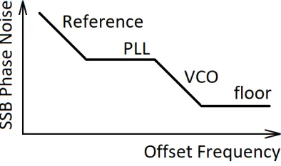
Figure 1.4Sketch of the SSB phase noise of a free-running VCO.
Since a real signal has symmetrical spectrum, we can observe the SSB spectrum of a VCO output
signal, which can take the form of Fig. 1.4. The random fluctuation in phase is shown as side band,
and fluctuations concentrated at a certain frequency can manifest as spurs. The center frequency is
where the signal power is most concentrated, and the X-axis is the frequency offset to the center,
usually shown in logarithmic scale. The reported phase noise is often taken at an offset spot from
the plot that is of interest to the specific application.
Starting from a far-off offset frequency, the SSB phase noise curve is flat, reflecting the power
ratio of noise to the main oscillation signal. As the offset frequency is lowered, the resonator Q begins
to have a growing impact on the total random nonlinearity, which results in a 20 dB/decade roll-off
region. As the offset frequency moves towards a transition frequency where there is significant 1/f type of noise sources influencing the resonator, this 1/f feature adds up to the 20 dB/decade and results in a 30 dB/decade roll-off region. Usually, this 1/f transition frequency is lower than the resonator Q-influenced frequency, which results in the existence of 20 dB/decade region without a
10 dB/decade region.
Frequency multiplier and divider can modify the VCO output frequency to another frequency
which has a integer ratio with the VCO. There are many different types of topology and
implementa-tion for the frequency translaimplementa-tion circuits, with stand-alone circuit blocks being the most common.
active device and rely on efficient extraction of the harmonic signal. Frequency dividers can take
the form of a high-speed digital logic, e.g. current-mode logic, in the millimeter-wave regime. If
matching is well taken care well, these implementations can have a very wide bandwidth. These
implementations produce additive noise on top of the signal input, which raises the noise floor.
But they usually do not raise the phase noise in the 30 dB/decade or 20 dB/decade regions, as the
additive noise produces much less extra phase fluctuation than what is already in the input to the
multiplier and divider. The result in phase noise is then shifted by+20 logfo/fi in dB (numerically, 6 dB/octave), withfo/fibeing the multiplication or division factor.
Another type of frequency translation circuit is the injection-locked multiplier and divider. These
require a separate VCO at a harmonic or sub-harmonic of the input signal. Because a free-running
VCO has a certain frequency range within which it will resonate with the input harmonic, the
new VCO can act as a frequency multiplier and divider. Unfortunately, the free-running VCO can
sometimes have a much narrower locking range. Because usually the new VCO is free-running, and
the input is already controlled by reference which has a much better phase noise, the phase noise in
this case will also follow the input with a shift of 6 dB/octave.
The millimeter-wave signal is eventually locked to a frequency reference, which is from a crystal
oscillator in the MHz range for a typical product. The frequency needs to be multiplied to the
targeted millimeter-wave range, where a phase-locked loop turns out to be useful. The PLL utilizes
the divider for frequency multiplication by using a feedback loop, in which a higher frequency is
generated by a VCO, then down-converted by a divider chain, and compared with the reference
phase or frequency to adjust the VCO control voltage, until the divided frequency and the reference
are matched. For a MHz reference, a PLL can use dividers implemented as the digital logic, so it
is flexible to take real-time control of the output frequency, even when the output frequency is a
fractional multiple of the input and more complex cases.
The phase noise of the output signal is also a function of the loop bandwidth. Compared to
the VCO output, the PLL is able to suppress the phase noise at an offset frequency within the loop
bandwidth, and will reflect the crystal reference by the 6 dB/octave shift at a frequency closed-in
to the center. Outside of the loop bandwidth, the phase noise of the VCO itself will be manifested.
Overall, the phase noise can be dominated by phase-locked loop (PLL) reference frequency in a
Figure 1.5Sketch of the SSB phase noise of a PLL output.
both VCO and subsequent high-frequency circuit at the noise-floor (roughly>100 MHz). On the
one hand, a smart choice of the PLL loop bandwidth picks the lower phase noise in both regions,
whereas this choice may also depend on specific application requirement. On the other hand, the
intrinsic phase noise of both PLL and VCO need to be minimized for optimum performance. This
study mainly deals with phase noise of the VCO, and the offset frequency is usually chosen at 1 MHz,
where VCO is the key contributor of phase noise.
Since the PLL output is from the VCO, its harmonic components are under control, but the
output may still suffer from spurious response due to the reference and control logic clock. Using
two cascaded PLLs may solve the problem of spurious response, as the final output is first locked to
an intermediate frequency which in turn is locked to the crystal reference. In this way, the spurs due
to reference is only present in the intermediate frequency, but the loop bandwidth of both PLLs
need to be chosen carefully.
For millimeter-wave frequency synthesis, division ratio between output and reference is very
large which is hard to control, especially if the reference is low or fine frequency step is needed.
The large division ratio is also bad for PLL phase noise as the flicker noise can be up-converted
to a much higher offset frequency. One approach to solve such a problem is by using offset PLL,
which uses a mixer to down-convert the VCO output or after the prescaler directly to a much lower
frequency. This approach may take a longer delay to obtain locking of the output, but it controls the
output frequency accurately.
Instead of using PLL, lower frequency RF signals can now be generated using direct digital
frequency synthesis (DDFS). DDFS uses a digital processor to calculate or look up the instantaneous
waveform. This allows the generation of frequency-agile signals with very wide bandwidth coverage
and low harmonic distortion. DDFS has become especially popular as the DAC speed is increased
significantly, and is also bounded by the limit of the DAC speed, whereas power consumption can
also be an issue.
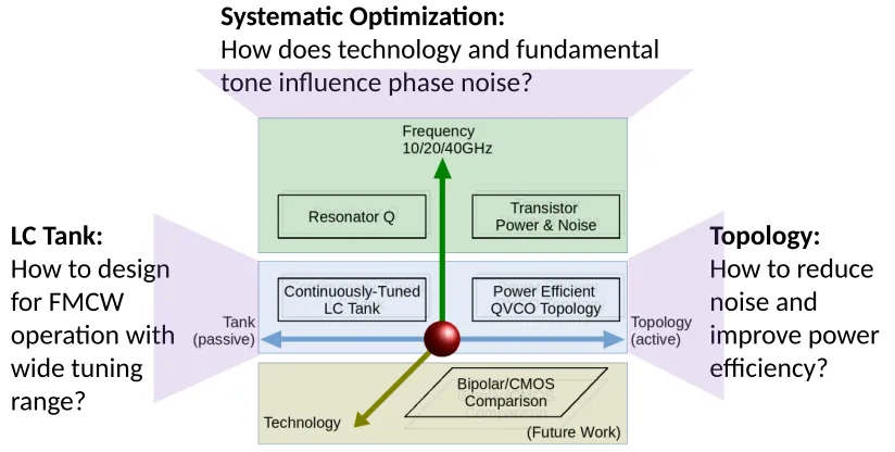
1.3
Research Objectives
In the context of the issues discussed above, this dissertation starts by establishing a thorough
understanding of millimeter-wave VCOs specifically for radars, from the aspects of their tuning range
and phase noise, respectively. First, radars require a wide tuning range to improve the resolution
of range and velocity measurement, and they also require the frequency to be tuned continuously,
which results in a high tuning gain. From a circuit perspective, it is imperative to eliminate noise
coupling to the tuning voltage, which ensures the VCO has lower phase noise. Second, the radar
receiver sensitivity requires low phase noise from the VCO. A quadrature VCO can potentially
reduce the noise injection from the transistors, and a good VCO topology should also improve the
power efficiency. With these understandings, this dissertation continues to push towards a globally
optimal solution. The passive device should be optimized in regard to the physical properties of the
fabrication process to make the most of on-chip resources. Benefiting from an additional variable
to choose the fundamental tone of the VCO, passive and active devices should also be discussed
in terms of their frequency properties to minimize phase noise. The overview of the goals and
approaches taken in this systematic optimization study is shown in Fig. 1.6.
Chapter 3 focuses on the technique to eliminate noise coupled to the tuning voltage for wide
tuning range VCOs. VCOs whose frequency can be continuously-controlled over a wide tuning range
find many applications, including frequency-modulated continuous-wave (FMCW) radar,
chirped-pulse millimeter-wave spectroscopy, and even stabilized sources with widely tuned frequency band.
Since this wide continuous tuning range feature translates to a high tuning gain (KV C O), a problem arises that requires the tuning voltage to be noise free to avoid excessive amplitude-modulated
to phase-modulated (AM-PM) side band in the form of phase noise. According to[HA03] [Bon06],
the excessive phase noise due to noisy tuning voltage deteriorates as the tuning gain increases,
frequency-Research Objectives
LC Tank:
How to design
for FMCW
operation with
wide tuning
range?
Topology:
How to reduce
noise and
improve power
efficiency?
Systematic Optimization:
How does technology and fundamental
tone influence phase noise?
11/16/17 8
Figure 1.6Overview of the approaches to the systematic optimization of millimeter-wave VCOs.
modulated continuous-wave (FMCW) radar, which ends up having separate VCOs to cover low
phase noise for long-range radar (LRR) and wider tuning range for short-range radar (SRR)[Tro12],
resulting in a larger chip area. A workaround is valid only for stabilized frequency sources which can
have multiple digitally-switched bands to reduce the tuning gain of each band. Thus, it is necessary
to investigate techniques to render the tuning voltage noise free for a wide continuous tuning range
VCO.
Chapter 4 focuses on a novel quadrature topology for lower phase noise and higher power
efficiency. As the frequency goes up into the millimeter-wave range, it becomes more challenging
to balance the trade off between phase noise and power efficiency of the VCO. Intuitively, this is
reflected in the observation of figure-of-merit (FoM) which is a combined indication of phase noise
and power consumption, as most VCOs with an absolute value of figure-of-merit (FoM) higher than
190 dBc/Hz are found at around or lower than 10GHz. On the one hand, since VCO has to be biased
consistently in the state that offers good phase noise, power efficient VCOs in the end will drive
down operating cost and improve mobility. But for high-performance millimeter-wave applications,
this goal should not be obtained by sacrificing phase noise. On the other hand, both phase noise and
power efficiency of the VCO are poised to be hindered as the frequency goes up. Materials generally
become more lossy, the parasitic capacitors become lower impedance, and the power efficiency of
higher direct-current (DC) current is needed to maintain the power level of oscillation. It is thus
necessary to investigate techniques to mitigate the power efficiency reduction for millimeter-wave
VCOs.
Chapter 5 discusses the frequency characteristics of passive and active structures and their
dependence on the fabrication process. With the availability of frequency multipliers and dividers,
it is not uncommon to select the VCO fundamental frequency at a sub-harmonic or super-harmonic
of the LO to improve phase noise. Yet the optimum remains unclear as existing design preferences
vary. The related choices on the fundamental frequency have been either studied or implied through
some efforts to reduce phase noise and power consumption, including the PLL and LO system
design[EH17] [Elb12] [CL13], the comparison of VCO topology[And05] [Gar14], and the modeling of
empirical VCO design[Ela14]. The power consumption is more relevant to the LO block structure,
whereas the optimum solution for phase noise has not been articulated with a physical explanation
in the existing approaches. This optimum solution is also believed to be governed by the parameters
of the fabrication process, so it is possible to develop a numerical model useful to predict phase
CHAPTER
2
MILLIMETER-WAVE VCO TECHNIQUES
To obtain good phase noise, the VCO design techniques need to be carefully investigated in several
aspects. The passive resonator should have a high Q to preserve energy and reduce loss. The active
circuit decides the amount of feedback to be injected back into the resonator to combat its loss,
so the right amount and low noise operation are critical design issues. The power of oscillation
signal is also influential as it allows more energy from the power supply to be turned into signal
than unwanted noise. Furthermore, the transistor used in the active circuit can significantly impact
the optimum oscillation power level, the location of noise sources, and the power efficiency.
In this chapter, discussions will first revolve around the specifications to characterize VCO
performance, then continue with the existing techniques on tank Q and active topology, and finally
2.1
VCO Performance Specifications
The voltage-controlled oscillator (VCO) as part of the local oscillator (LO) provides the carrier signal
for both communication and radar applications. It is required for VCOs to have low phase noise,
high power efficiency, and wide tuning bandwidth. Other VCO specifications exist to describe how
well the VCO works together with other circuits, including supply pushing, tuning gain (or tuning
sensitivity), and output power level. These specifications are sometimes at odds with each other, so
designers need to consider the trade-offs between them.
The tuning range and good passive Q usually do not co-exist. Since the varactor Q is low, when
wide tuning range is required, the varactor needs to couple more strongly into the tank, bringing
along with its loss due to its low Q. This phenomenon is exacerbated when the noise on the tuning
and supply voltage is coupled to the varactor, if the varactor size is large.
Another trade-off is between oscillation power and phase noise. The phase noise becomes
superior when the increase in signal power is not accompanied by the same level of noise power up
to a point. This phenomenon can be utilized to improve phase noise when power consumption is
not an issue, and for a low-power design, certain technique for a high-power design may no longer
be applicable.
The fundamental tone of existing VCOs appears at different frequencies and can lead to different
phase noise performance. This is an advantage as sometimes the VCO can be built at a sub-harmonic
of the local oscillation frequency, with the frequency multipliers and dividers being available to
transform the VCO frequency to an intended frequency, and eventually leading to better performance
in phase noise and tuning range. The tuning range can also become worse as the frequency goes up,
which is another reason to build VCOs at a lower frequency range. However, the VCO passive device
may occupy a smaller area, and it is believed in some cases that the inductor Q may become higher
as frequency goes up.
The question thus emerges as which frequency is the global optimum. This is to be addressed in
this study with a thorough understanding required of the technique to minimize phase noise. The
numerous kinds of VCO topology proposed for the VCO also need to be compared and improved if
necessary. Besides, the fabrication technology may influence the VCO performance via the passive
Difficulties lie in the trade-offs between the key performance of phase noise, tuning range, and
power consumption, which may be collectively compared. A figure-of-merit (FoM) can be used to
scale the overall performance by considering more than one particular specification.
One FoM is defined as
FoM=L ∆f+10 log P
D C 1mW
−10 log f
0 ∆f
2
(2.1)
to normalize the power dissipation and frequency parameters, whereL(∆f)is the phase noise, PD C is the DC power dissipation,f is the osculation frequency, and∆f is the offset frequency.
Another figure-of-merit, FoMT, which includes the impact of tuning range, and is defined as
FoMT =L ∆f
+10 log P
D C 1mW
−10 log f
0 ∆f
2
−10 log T R
10% 2
(2.2)
whereT Ris the tuning range.
2.2
The LC Tank
The oscillation frequency of an LC tank can be derived by observing the pole frequency of the
impedance expression. For a second-order LC resonator, this is
f0=
1
2πpLC, (2.3)
whereLis the inductance andC is the capacitance of the tank.
The tank Q is a property of the passive components that reflects its ability to store energy instead
of dissipate energy, and it can be evaluated using various methods. For a second-order LC resonator,
the tank Q is related to the inductor Q,Qi n d, and capacitor Q,Qc a p, by
Qt a n k=
Qi n dQc a p Qi n d+Qc a p
. (2.4)
Zi n d orZc a p, for a frequency far away from its self-resonance, by
Qi n d=Im(Zi n d) Re(Zi n d)
, (2.5)
Qc a p=
Im Zc a p
Re Zc a p
. (2.6)
It is interesting to note thatQi n dandQc a pusually do not strongly depend on the value of inductance and capacitance alone, as the Q does not change if multiple identical components are placed in
series and in parallel. Instead, their Q values depend on the structure and size of the components.
The existing designs of inductors and capacitors will be reviewed in this section.
A significant amount of work is conducted to improve inductor Q and to accurately model
the on-chip inductors, which is usually implemented as a spiral shape. For differential VCOs, a
symmetric inductor can have higher inductor Q than two identical single-ended inductors on each
side, due to the mutual coupling of the inductor winding sections.
On the modeling of inductance,[Gre74]is written decades ago but its influence is found for
on-chip inductors design up to this day. The study deals with sophisticated shapes by cutting it into
pieces with simpler geometries, and putting them together by considering the mutual inductance.
Since the formulas for simpler geometries were existing knowledge already and had been verified at
the time[Gro24], this later work utilized the result and produced useful insights. The work acts as a
primer for inductor design, as it elaborates on details of a classical engineering solution.
In another work,[Moh99]gives an analytical expression to calculate the inductance as a function
of the geometry. The work expands on the Wheeler Formula to tackle various shapes and multiple
turns. Also, the computation method with a sample computer program is introduced to model
inductance as accurately as possible, aiming to expedite EM solvers. The result is compared with
measurement with good agreement, and the approach introduced in the work has been exercised
by many other authors, validating the approach.
For mutual inductance,[Cha00]introduces a method for analytical calculation that leads to a
relatively accurate method with physical explainable result. The mutual inductance existing between
inductor coils is an essential part of the on-chip transformer. The work is based on Neumann formula
of the transformer in practice.
In[Shi06], the mutual inductance is calculated for multiple-level transformers and inductor
pairs with more complex geometries. The work utilizes the formulas of simpler shapes, obtained by
following[Cha00]as an example, and combines them to form the entire model using superposition
rules. This resembles the thought of superposition in[Gre74], only that it takes reasonably more
effort to find the incremental mutual inductance.
The loss of the metal line is modeled in[EE93]using analytical expressions with distributed
resistance-inductance-conductance-capacitance (RLGC) models. The properties of metal line are
studied for interconnects between circuit blocks, but the formulas also apply to inductor designs.
Although the expressions provided in the study is not entirely innovative at the time of publication,
it is presented in a useful way for future research. Also, the frequency range of model accuracy is
extended to 20 GHz which is considerably higher than most other works at the time of publication.
Another pioneering work is[Whe77]which gives the detailed equations for a microstrip line.
For circuit simulation, theπ-model is widely used in studies beginning in the late 1990s, in-cluding[NM97] [LC97] [Nik98]. These studies do not necessarily have the same equations used for
each element in theπ-model, but they do show a basis for circuit representation of the complex impedance response. The accuracy and bandwidth of the model is dealt with in later works[KP00],
which is suitable for a real circuit application.
The ground shield can be used for an on-chip inductor to partially reduce the coupling to
substrate, and this is studied in[YW98] [BR03]. It is shown the ground shield may cause either a
minor increase or decrease in inductor Q, and it will certainly increase the parasitic capacitance
slightly. Even though it may decrease Q by a little bit in certain occasions, experience suggests the
ground shield is better for achieving performance consistency and model-hardware agreement.
Various materials and patterns are also studied in[Ng02], and a method is also given to increase Q.
The metal skin effect needs to be modeled accurately to obtain good result.[Fer96]works on
a mathematically regular shape, leading to useful analytical result. More works need to be done
to deal with the issue when the cross-section is rectangular instead of circular.[Ant99]has some
insights about the impedance of inductor with rectangular cross-sections, and it is discussed under
the scope of Wheeler’s formula. Finally,[Ger09]simplifies the analytical calculation.
[Mel02]shows a way to obtain wide band inductor model using mutual coupling to the substrate
network.[Wei02]and[WL04]show another perspective on the modeling of the substrate loss, which
features more physics-based explanation and insight.[NM05]utilizes the EM tools and shows a
method to facilitate the automation of practical inductor design.[Huo06]serves as an example
of utilizing the existing knowledge on inductors to derive useful and accurate models for
radio-frequency integrated circuit (RFIC) applications.
The transformer models have become useful as more designs start to adopt transformers for
circuit improvement. The transformer can be used to save space in the place of multiple inductors,
and it may also be used as a coupling device between different circuit parts.[ZA98]is an early
example of using transformer in an RF low-noise amplifier (LNA), in which the design of the
trans-former is shown in detail.[Lon00]and[Sen14]show a method to obtain accurate model for the
transformer, and the parameter extraction method is also explained.[Vis14]shows an example
of using transformers in VCO design to improve the frequency selectivity, and it shows how the
transformer design criteria are reached.[Zha14]shows the transformer being used in a mixer to
improve transconductance and linearity.
For capacitors, the innovation is somewhat restrained compared to the inductor innovation, as
part of the capacitor modeling problem is shifted to the provider of the process design kit.[Vic05]
is devoted to deriving an accurate and scalable model of varactor. One main problem related to
capacitor is the limited Q of varactor, which is a component with a varying capacitive reactance as
a function of applied voltage. To deal with the limited Q, one way is to use a fixed capacitor with
higher Q, in series or in parallel with the varactor, so the overall capacitor Q is higher. The other
approach which works in a lower RF frequency is to use switches along with fixed capacitors to
realize digital bands, and this approach provides both variable capacitor and reduced tuning gain
within one band. In[SH10], switches are used with both inductor and varactors to expand the tuning
range to 157%.
But for the millimeter-wave frequency range, these two approaches start to show drawbacks. The
switches themselves have higher loss, and the total tank capacitance is expected to decrease with
the parasitic capacitance unchanged, leaving less room for a high-Q fixed capacitance. Hence, some
other works are performed focusing on the increase of individual varactor performance.[Mag01]
shallow isolation trench. A higher varactor tuning ratio is good for obtaining higher tuning range.
[XO08]increases varactor Q by pushing to the verge of design rule.
Recently, LC tank with multiple resonant frequencies are explored for performance improvement.
In[KL05], a transformer is used to increase the oscillation amplitude of a low-power, low-supply
VCO, essentially forming a fourth-order LC tank. In[Tch07], a fourth-order LC tank is implemented
with series switched inductor to realize a dual-band VCO. In[Wu13], a technique known as
negative-capacitance is realized by placing an extra capacitor at the opposite side of the cross-coupled
transistor pair. The technique is used to reduce the size of the fixed capacitance thus achieving a
higher tuning range. In[BS13], a transformer is used in a fourth-order LC tank to obtain a oscillation
waveform that has rich components in both resonances. The two frequencies are designed at
fundamental and third-harmonic, respectively, essentially forming a class-F oscillator. It shapes
the waveform such that the noise injection from the transistors contributes less to phase noise.
In[Baj15], transformers are used in quadrature oscillators to achieve both quadrature coupling
between two differentials and two different oscillation frequencies for expanding the tuning range.
2.3
Types of VCO Topology
Figure 2.1Schematic of a simple cross-coupled VCO with external biasing.
Figure 2.2Schematic of two variants of a Colpitts VCO: the common-collector variant (left) and the common-base variant (right).
improved version are built. The cross-coupled structure in Fig. 2.1 is essentially a differential-pair
with positive feedback to provide the negative transconductance. For bipolar technologies,
AC-biasing of the transistor is needed for better control of the power consumption and for better phase
noise. The Colpitts topology in Fig. 2.2 uses feedback capacitors from the collector to either base or
emitter to obtain better impedance matching for both higher power efficiency and better phase
noise. For bipolar technologies, the Colpitts structure can be designed with lower phase noise
compared to the cross-coupled because of a lower external base resistance, but it usually costs a
higher bias current to obtain the same oscillation amplitude.
The VCO power efficiency can be improved by boosting the transconductance (Gm) of the
active circuit, namely maintaining the same Gm with a reduced bias current. For this goal, design
techniques are divided into two categories depending on the signal power levels. One category
focuses on ultra-low-power applications, including short-range and wearable technology, with
con-straints on phase noise also relaxed by 10 dB. The other category concentrates on high performance
millimeter-wave application, which requires the VCO to not only have superior energy efficiency
but also have low phase noise. This categorization is not black and white, but it can be attributed to
the trade-off between phase noise and power consumption in general.
For high performance VCO, Gm-boosting works by modifying the VCO topology, including
enhanced transformer feedback[Wan11] [Liu10] [NL12], among others. A recent approach for CMOS
technology, called current reuse[Ha14] [Cha14], replaces the n-channel metal-oxide
semiconduc-tor (NMOS) transissemiconduc-tor differential-pair with one NMOS and a folded-up p-channel metal-oxide
semiconductor (PMOS) transistor, aiming at doubling the Gm with the same bias current.
To neutralize the impact of this trade-off during the evaluation of the circuit topology, the
figure-of-merit (FoM) suggests that the phase noise and power consumption can be scaled via
biasing of the implemented circuit, until the breakdown voltage is reached or other limitations arise.
Meanwhile, the FoM of a VCO topology also considers the tank Q and transistor Gm, which can be
influenced by the oscillation frequency. Since both Q and Gm are suspected to drop when frequency
goes up into the millimeter-wave range[Mur16] [HSN15], it indicates a potential aspect of FoM
improvement. Although a considerable number of VCOs are built at a sub-harmonic frequency
followed by frequency multipliers[Liu04] [TH12]for the same reason, including this study, it should
not prevent us from exploring ways to improve FoM in the millimeter-wave frequency range.
2.4
Theoretical Phase Noise Studies
Other than these practical approaches for building better VCOs, theoretical approaches are following
a separate yet indispensable path for obtaining a deeper understanding of VCO designs.
The Barkhausen stability criterion is a classic theory that applies to VCO designs. It states
the necessary criterion in both amplitude and phase for oscillation to build up, although it does
not directly explains the phase noise. However, by observing the tank impedance, the magnitude
criterion can be satisfied within a much larger bandwidth than the phase criterion, so the Barkhausen
criterion does indicate the phase criterion to be a more frequency-distinguishing factor of oscillation
frequency.
Leeson’s equation[Lee66]correctly points out the various factors affecting phase noise, including
tank Q, signal power, active circuit, and other related frequency parameters. It also serves as a basis
for further phase noise analysis, and it can potentially lead to very accurate phase noise estimation.
In this study as well as many others, Leeson’s equation finds many opportunities to properly explain
To describe how strongly the signal can be influenced by noise within a waveform cycle, the
impulse sensitivity function (ISF) is defined as a function of the voltage waveform, and calculation
methods are given. This theory is originally introduced in[HL98]and it articulates the influence of
noise sources depending on the instantaneous voltage within a cycle of the waveform. From another
perspective, the conversion of noise is studied at their different harmonic components. This study
also serves as a foundation of many modern works on millimeter-wave VCO phase noise analysis.
The virtual damping[HH02]describes the fundamental physics of phase noise through the
Ein-stein relation. This theory can be regarded as an in-depth extension of ISF model, but it unfortunately
CHAPTER
3
SPLIT-INDUCTOR TUNABLE
RESONATOR
The local oscillator (LO) phase noise is a critical circuit for W-band frequency-modulated
continuous-wave (FMCW) automotive radars. Good phase noise improves the receiver sensitivity due to its
inevitable leakage to the receiver, especially for long-range radar systems. At the same time, the
transmitted frequency needs to cover a wide bandwidth especially for short-range radar systems to
improve the range resolution. The sensitivity and wide bandwidth requirements are not mutually
exclusive for a high-performance millimeter-wave radar transceiver.
In addition, it is desired to realize a voltage-controlled oscillator (VCO) with low phase noise
and wide tuning range for a “multi-mode" long-range and short-range radar, which is helpful for
reducing area and energy consumption. Contrary to this notion, two separate oscillators were used
[Tro12], one which optimizes the phase noise for long-range radar operation at 76 to 77 GHz and
the other which optimizes the tuning range for short-range radar operation at 77 to 81 GHz. This is
to the phase-modulation conversion from amplitude-modulation noise sources. The highKV C Ois owing to the use of large variable-reactors (varactors) necessary to cover the available spectrum for
FMCW operation, which forbids the use of digital band switches.
3.1
Requirement of FMCW Generator
Many millimeter-wave VCOs with a highKV C O are reported to have specific means to prevent noise sources from coupling to the varactor control voltage. In one technique, filtering in the
form of a degeneration inductor[LR03]or a bypass capacitor[MA08]can reject high-frequency
noise components from a tail current source. Not only for high-frequency, the low-frequency noise
component must also be separated from the inductor-capacitor (LC) tank. For this purpose, in the
AC-coupled tank structure[Flo08], a large series capacitance is added to block the low frequency
coupling path to reduce supply pushing and AM-to-PM noise conversion from bias voltages, as
shown in Fig. 3.1. However, AC-coupled varactors require a high-impedance path on one side of
the varactor tuning voltage, and when a resistor is used, we can see significant phase noise coming
from its thermal noise due to the highKV C O. As a result, a low-loss but high-impedance coupling approach, e.g. an RF choke, is preferred for AC-coupled varactor. When this RF choke takes the form
of an inductor[Lev16]or a microstrip line[TT12], they can be bulky and parasitic-rich. A better
alternative with a smaller footprint is to use the transformer along with an AC-coupled varactor,
which uses the primary winding for transistor current supply and the secondary winding for varactor
coupling, and together they provide the inductance needed for resonance[Wan14]. In essence, the
primary and secondary windings act as if it were a single inductor at high frequency, but split in
the middle plane for separate DC voltages. As the advancement in fabrication provides thicker
metal stacking, the transformer resonator is helpful for reducing the noise coupling to the varactors,
thereby reducing the phase noise associated with highKV C O.
On the other hand, the quality (Q) factor of the transformer tank needs to be optimized to
further reduce phase noise. Yet the transformer-coupled resonator is a complex structure requiring
a detailed analysis and design methodology, which can possibly lead to some insights. Moreover,
the transformer-coupled structure is also found to work with the capacitive AC-coupling, with only
in between[Bev07] [Tch07]. Since the transformer LC tank has been analyzed with magnetic-only
coupling, we need to expand the analysis to include the capacitive coupling.
With impedance analysis, it is found that the strong capacitive coupling, also known as a
split-inductor tunable resonator (SITR), shows a more consistent Q over the wide tuning range than
a generic transformer tank. For the case of SITR, the impact of magnetic coupling needs to be
modeled more accurately including its loss, since the parasitic and loss play a greater role as the
frequency goes up. With extensive electromagnetic simulation, we demonstrate an approach to
obtain the transformer parameters more accurately and conveniently by reusing our prior knowledge
of individual inductor winding.
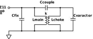
Figure 3.1Simplified schematics of the AC-coupled varactor (left) versus the split-inductor tunable res-onator (right) used within differential Colpitts VCO.
Owing to the high tuning gain, three mechanisms can cause the VCO to be sensitive to noise on
the bias lines. To handle these mechanisms, the available options will be discussed in detail in this
section.
First, noise on the bias and tuning voltages, especially their low-frequency component, may
couple to the varactor thus modulating the output frequency. As was introduced, the transformer