ABSTRACT
MOODY, BAXTER FINLEY. Strained Layer Superlattice Solar Cells. (Under the direction of Dr. Nadia El-Masry and Dr. Salah Bedair.)
For several years, photovoltaic researchers have searched for a material to extend solar cell absorption to wavelengths beyond the GaAs cut-off to increase efficiency of multi-junction solar cells. The best record efficiency of any solar cell is currently ~40% for a 3-Junction GaInP/GaAs/Ge cell at high solar concentration manufactured by Spectro-Lab. Higher efficiency can be realized with a 3-Junction GaInP/GaAs/1eV or 4-Junction GaInP/GaAs/1eV/Ge configuration if a high quality, lattice matched 1eV material can be found. The best material candidate for several years has been InGaAsN due to a very large bandgap reduction with small N concentrations, but quality and performance remains low despite considerable effort by many researchers to improve the material to adequate device quality. In particular, the carrier diffusion lengths are greatly reduced compared to GaAs due to poorly understood defects. For very low N compositions, below ~1%, device quality is maintained.
Here a novel solution is proposed to develop a high quality material that is both lattice matched to GaAs and has a bandgap around 1eV. By inserting a
strain-layer-superlattice of In0.28Ga0.72As/GaAs0.25P0.75 into the i-region of a GaAs p-i-n diode, effective
subsequent growth of a tensile strained GaAsP layer, which is also below the critical layer thickness. This structure is then repeated for several periods to build up total InGaAs thickness for increased photon absorption. Thin GaAsP barriers are required for effective carrier collection which imposes a high P composition for strain balance. Cells with thick barriers exhibited low currents, indicating that carrier tunneling is critical for proper device performance. Solar cells demonstrated in this research effort are at least equal in
Strained Layer Superlattice Solar Cells
by
BAXTER FINLEY MOODY
A dissertation submitted to the Graduate Faculty of North Carolina State University
in partial fulfillment of the requirements for the Degree of
Doctor of Philosophy
MATERIALS SCIENCE AND ENGINEERING
Raleigh, NC 2006 APPROVED BY:
BIOGRAPHY
ACKNOWLEDGEMENTS
CONTENTS
LIST OF TABLES... vi
LIST OF FIGURES... vii
1 INTRODUCTION... 1
1.1 World Energy Overview... 1
1.2 Current and Future Role of Photovoltaic Technology... 4
2 PHOTOVOLTAIC BASICS... 8
2.1 Solar Irradiance... 8
2.2 Semiconductor Materials Properties... 10
2.2.1 Crystal Structure...10
2.2.2 Energy Bands in Semiconductors...13
2.2.3 Electrons and Holes...17
2.2.4 Junctions...22
2.3 Device Principles ... 23
2.3.1 Photocurrent, Dark Current, and Photovoltage...23
2.3.2 Fill Factor and Efficiency...26
2.3.3 Cell Design Considerations ...29
3 MULTI-JUNCTION SOLAR CELLS... 32
3.1 Lattice Matching... 33
3.2 Materials for Multijunction Photovoltaics... 36
3.2.1 Candidate PV Semiconductors for High Efficiency ...36
3.2.2 Survey of Developed PV Materials Systems...39
3.2.3 Pursuit of a 1eV Lattice Matched PV Junction...42
4 PROPOSED NOVEL THIRD JUNCTION... 45
4.1 Strained Layer Superlattices ... 45
4.2 Survey of InGaAs/GaAsP Structures for Photovoltaics ... 48
4.3 Analysis of InGaAs/GaAsP SLS for PV Applications... 48
4.3.1 Bandgap Dependence on Strain, Temperature, and Composition ...49
4.3.2 Critical Layer Thickness for InGaAs and GaAsP...54
4.3.3 Quantum Size Effect...57
4.3.4 p-i-n Device...62
5 OMVPE GROWTH... 70
5.1 Organometallic Precursors... 71
5.2 OMVPE Growth Equipment... 72
5.2.1 Precursor Sources and Delivery ...73
5.2.2 Reactor ...77
5.2.3 Exhaust System and Scrubber ...82
5.2.4 Equipment Cleanliness and Film Purity ...85
5.3 Growth Conditions and Procedures ... 88
5.3.1 GaAs Substrates ...89
5.3.3 Film Growth Details ...91
6 CHARACTERIZATION... 97
6.1 Optical Microscopy ... 97
6.2 X-Ray Diffraction... 101
6.3 Photoluminescence ... 106
6.4 Hall Effect... 108
6.5 Current-Voltage and Spectral Response... 109
6.6 Transmission Electron Microscopy ... 111
7 DEVICE PROCESSING... 113
7.1 Photolithography... 114
7.2 Metallization and Liftoff... 116
7.3 Etching... 117
7.4 Annealing... 118
8 GAASN ... 119
9 STRAINED LAYER SUPERLATTICE SOLAR CELLS... 125
9.1 Development of the InGaAs/GaAsP SLS... 125
9.2 Device Performance... 133
9.2.1 Light and Dark Current ...135
9.2.2 Spectral Response...139
9.2.3 Carrier Transport ...141
10 CONCLUSION... 149
REFERENCES... 151
APPENDIX... 165
APPENDIX A... 166
LIST OF TABLES
Table 1.1 Available Primary Energy Sources... 2
Table 2.1 Selected Semiconductor Parameters ... 21
Table 4.1 Parameters for Electric Field Calculation ... 65
Table 5.1 List of Precursors ... 92
Table 5.2 Bulk Film Growth Parameters ... 93
Table 5.3 Quantum Well Growth Parameters... 94
Table 9.1 Performance Parameters for Test Cells Under AM1.5D Illumination ... 138
LIST OF FIGURES
Figure 1.1 Record Cell Efficiencies... 6
Figure 2.1 Standard AM0 and AM1.5 Direct Spectra ... 10
Figure 2.2 Face Centered Cubic Unit Cell... 11
Figure 2.3 Zinc Blende Structure... 12
Figure 2.4 Energy Band Formation as Atoms are Brought Together to Form Solids ... 14
Figure 2.5 Energy Band Structure of Si and GaAs (After Chelikowski38 and Cerdá39) Arrows Indicate Indirect Transition in Si and Direct Transition in GaAs... 16
Figure 2.6 Simplified Diagram of Valence and Conduction Bands, Bandgap, and Electron and Hole Behavior at Absolute Zero and Finite Temperatures ... 18
Figure 2.7 Photogeneration of Carriers... 19
Figure 2.8 Acceptor dopants enhance conduction in p-type semiconductors via creating holes in the valence band. Donor dopants enhance conduction in n-type semiconductors via promoting electrons to the conduction band... 20
Figure 2.9 p-n Junction Formation and Resulting Band Structure ... 23
Figure 2.10 Diode Characteristic I-V Curve... 24
Figure 2.11 Maximum Power Rectangle or Fill Factor ... 26
Figure 2.12 Equivalent Circuit & Parasitic Resistances ... 27
Figure 2.13 Limiting Efficiency for Single Junction Solar Cell. Verified Record Efficiency for GaAs and Si Indicated in Red ... 29
Figure 2.14 Typical Solar Cell Design ... 31
Figure 3.1 Lattice Mismatch Strain Relaxation via Formation of Dislocations ... 34
Figure 3.2 Critical Layer Thickness as Predicted by Matthews-Blakeslee and People-Bean ... 35
Figure 3.3 AM1.5D 2-J Cell Thermodynamic Limiting Efficiency Contours (Maximum at 1.56eV and 0.93 eV) ... 37
Figure 3.6 AM1.5D Efficiency Contours for 4J Top/GaAs/3rd/Ge Cell... 41 Figure 4.1 Strained Layer Superlattice with Resulting Band Diagram ... 47 Figure 4.2 Band Structure of GaAs under (A) Biaxial Compressive Strain, (B) Zero Strain,
and (C) Biaxial Tensile Strain (CB=conduction band, HH=heavy hole band, LH=light hole band, SO=split-off band)(After Asai130 and Bir129) ... 50 Figure 4.3 Compressive Strain Induced Light(Blue) and Heavy(Red) Hole Band Shift
Compared with Unstrained InGaAs Bandgap Dependence(Green) on In Fraction
(300K). Combined Effective Bandgap Shift is also Plotted in Black... 52 Figure 4.4 Tensile Strain Induced Light(Light Blue) and Heavy(Red) Hole Band Shift
Compared with Unstrained GaAsP Bandgap Dependence(X-Green, Γ-Dark Blue) on P Fraction (300K). Combined Effective Bandgap is Plotted in Black... 53 Figure 4.5 Critical Layer Thickness Indium Fraction Dependence for InGaAs Strained to
GaAs (After Matthews-Blakeslee)... 55 Figure 4.6 Critical Layer Thickness Phosphorous Fraction Dependence for GaAsP Strained
to GaAs (After Matthews-Blakeslee) ... 56 Figure 4.7 Band Structure of an In0.15Ga0.85As/GaAs0.7P0.3 SLS Demonstrating Quantum
Size Effect (Well and Barriers Layers are 100Å)... 58 Figure 4.8 Graphical Solution of the Schrödinger Equation to Find Quantized Energy States
in the InGaAs Quantum Well (Each zero represents a discrete energy level formed in the well in the valence band (Blue) and conduction band (Red))... 60 Figure 4.9 Combined Effective In0.3Ga0.7As Bandgap (Green) for a Range of Well Widths,
Unstrained (Blue) and Strained (Red) Bandgaps are Shown without Quantum Size Effect for Comparison (Barriers are GaAs0.2P0.8) ... 61
Figure 4.10 Quantum Size Effect for InGaAs Well Thickness (Effects of Strain,
Composition, and Temperature also Included in the Calculation) ... 62 Figure 4.11 Electric Field Across a GaAs p-n Junction (NA = 2 x 10¹⁸, ND = 1.1 x 10¹⁷, xp =
7.62nm, xn = 139nm, E0 = 1.9 x 10⁵ V/cm) ... 63
Figure 4.12 Electric Field Extended Across i-Layer in a p-i-n Configuration (Dashed lines indicate the field behavior with increasing p-type doping in the i-layer) (NA = 2 x 10¹⁸,
ND = 1.1 x 10¹⁷, xi = 300nm E0 = 4.3 x 10⁴ V/cm) ... 66
Figure 4.13 Band Bending and Carrier Escape in the Presence of Built-In Electric Field Across i-layer( open circles = holes, solid circles = electrons) ... 68 Figure 5.1 Basic Components of an OMVPE Growth System (MFC = Mass Flow
Figure 5.2 Run/Vent Manifold Schematic... 75
Figure 5.3 Optical Micrographs(1000X) of Small Surface Features on GaAs from a Gas Phase Reaction (left) and a Smooth Surface for GaAs Grown after a Divider Plate was Added to the Growth Chamber to Seperate Gas Flows(right)... 78
Figure 5.4 Reactor Schematic... 79
Figure 5.5 Photograph of Reactor... 81
Figure 5.6 Optical Micrograph (1000X) of a GaAs Surface Grown at 70 Torr (Metallic Droplets are Presumed to be Unreacted Gallium) ... 83
Figure 5.7 Substrate Susceptor Coverage ... 84
Figure 6.1 Optical Micrograph (500X) Rough Surface of n-GaAs Caused by Low Growth Temperature (Arrow indicates a water stain from improper sample drying) ... 98
Figure 6.2 Optical Micrographs (400X) of Cross Hatching in (1) Compressively Strained In0.1Ga0.9As and (2) Tenisile Strained GaAs0.8P0.2, Plus the (3) Featureless Surface of a Strain Balanced In0.1Ga0.9As/GaAs0.8P0.2 SLS... 99
Figure 6.3 Cross-Section Optical Micrographs (1000X) of AB-Etch Delineated Interface and Edge Crown... 100
Figure 6.4 Optical Micrograph (400X) of Etch pits for InGaAs/GaAs Double Heterostructure and InGaAs/GaAs Strained Layer Superlattice ... 101
Figure 6.5 θ-2θ XRD Scan of a Thick GaAsP Film ... 103
Figure 6.6 HRXRD Rocking Curve of a GaAs0.985N0.015 Film on GaAs... 104
Figure 6.7 HRXRD Scan of a Slightly Lattice Mismatched SLS with Pendellosung Fringes ... 106
Figure 6.8 77K PL Scans of Thick Films of GaAs0.6P0.4, GaAs, and In0.3Ga0.7As ... 107
Figure 6.9 Current-Voltage and Spectral Response Test Apparatus ... 111
Figure 7.1 Contact Metallization Schemes ... 117
Figure 8.1 Effect of Carrier Gas on N Incorporation at 600°C... 120
Figure 8.2 Growth Temperature Dependence of N Incorporation in GaAsN ... 121
Figure 8.3 X-Ray Diffraction Data for Various N Compositions in GaAsN ... 122
Figure 9.1 XRD for Strained GaAs/GaAsP and InGaAs/GaAs and Strain Balanced
InGaAs/GaAsP SLS’s... 126 Figure 9.2 Optical Micrographs of Surfaces Corresponding to Each Sample in Figure 9.1
... 127 Figure 9.3 TEM of InGaAs/GaAsP SLS ... 128 Figure 9.4 XRD for an In0.14Ga0.86As/GaAs0.25P0.75 SLS with 83Å Wells and 28Å Barriers
... 130 Figure 9.5 XRD for an In0.28Ga0.72As/GaAs0.1P0.9 SLS with 38Å Wells and 23Å Barriers 131
Figure 9.6 PL for Various Compositions and Well Widths (Experimental data points are color coordinated with the corresponding calculated curves) ... 133 Figure 9.7 Typical Final Test Structure (SLS thickness ranged from 0.3μm to 0.8μm) .... 134 Figure 9.8 AM1.5D 1-Sun Light Current of Selected Test Cells A, B, C and D Compard to
GaAs Control Cell (A: In0.28Ga0.72As/GaAs0.25P0.75, 30 periods, 0.2μm, B:
In0.28Ga0.72As/GaAs0.1P0.75, 50 periods, 0.35μm, C: In0.28Ga0.72As/GaAs0.1P0.9, 50
periods, 0.3μm, D: In0.28Ga0.72As/GaAs0.1P0.9, 50 periods, 0.3μm) ... 136
Figure 9.9 Dark Current for Test Cells in Figure 9.8 ... 137 Figure 9.10 I-V of Doped SLS Devices (Dashed lines indicated reduced ISC and VOC typical
of doped structures. The corresponding undoped sample is plotted as a solid curve with matching color.)... 139 Figure 9.11 Spectral Response of Samples A(Green) and B(Red) Compared to the
Reference Cell(Black)... 140 Figure 9.12 Spectral Response of Highest Light-Current Cell and Reference GaAs Cell . 141 Figure 9.13 Partial Band Diagram for In0.28Ga0.72As/GaAs0.25P0.75 SLS with 38Å Wells and
1 INTRODUCTION
Energy demands of humans continue to increase as the population of Earth increases and more countries become industrialized. Simultaneously, the primary energy source, fossil fuel, is being depleted at a rate much higher than it is generated. A paradigm shift is inevitable for the energy model of the entire planet. Beyond this fact, there is a great deal of disagreement about the future of energy use and production for planet Earth. A thorough treatment of this topic is far beyond the scope of this work, but it merits a brief summary as it is the ultimate motivation for this research.
1.1 WORLD ENERGY OVERVIEW
Three main questions arise when analyzing modern energy supply and consumption. How long will fossil fuels meet our needs? How much energy will the planet ultimately need? What are viable alternative energy sources? Many clever individuals have
attempted to answer these questions,1,2,3,4 but the task is daunting. Aubrecht has assembled an overview of the topic5 which includes some 5400 references covering scientific works, government reports, environmental impact, politics, economics, conservation, and culture.
Estimates for the longevity of fossil fuels range from only a few years to thousands of years, but most predict a few hundred years. A major problem is estimating how much additional fuel will be found in addition to known reserves. Other concerns include
conserving fossil fuels for a myriad of useful, non-energy related products and protecting the environment from the harmful effects of combustion.
from 84 billion6 to 2 billion7 for fully sustainable energy. Energy demand per capita continues to increase which is a trend that can not continue indefinitely.
Accurately predicting future dominate energy sources is impossible, but we can identify several possibilities. Available energy sources are classified as either
non-renewable or non-renewable as in Table 1.1. Non-non-renewable resources can not be regenerated on a human time-scale while renewable resources are continually refreshed and available for a very long time.
Table 1.1 Available Primary Energy Sources
Non-Renewable Renewable
Fossil Fuels (Oil, Coal, Natural Gas) Hydropower
Nuclear Fission (Uranium) Biomass (Plants, Urban Waste) Nuclear Fusion (Deuterium-Tritium) Wind
Geothermal Solar
non-scientific and non-scientific debates to the point that it is not clear if it even exists. Therefore it will not be discussed here other than to point out that it may not produce exceedingly harmful waste like fission and hot-fusion. Geothermal energy can be renewable if the rate of extraction is low, suitable for a small local area. However, current large scale plants extract heat energy faster than it is supplied to the system.
Hydropower is by far the most utilized renewable energy source worldwide, primarily in the form of hydroelectric dams. Problems with this method include massive habitat and wildlife destruction in the flooded areas, safety for downstream residents, and reservoirs filling with silt. Burning plant matter such as trees is renewable if new plants are planted in place of those harvested. The new plants will also remove environmentally harmful CO2 produced from combustion, making this method environmentally safe.
However, there is simply not enough feedstock available to support even a significant fraction of world demand. Energy from wind comes primarily from windmills and is suitable only for areas with generally constant wind speed since lack of wind equals zero power and gusts are destructive. All of these sources can be classified as solar energy. For example, fossil fuels are solar energy in the form of organic matter, stored over millions of years. For the current discussion, solar energy refers to more direct use of solar energy such as direct thermal heating, solar electric, and photovoltaics. Solar energy is appealing
Each of these energy sources will play an increasingly significant role in the
inevitable demise of the fossil fuel paradigm. The primary end product of each is electricity which is suitable for stationary and grid-based power schemes. The current outlook for transportation energy requirements is grim by comparison. Automobiles and planes in particular benefit from the high energy density in petroleum fuels which provide relatively low weight, high power, and long operating distances. Current technology does not have a solution that will satisfactorily replace gasoline, diesel, and jet fuel. Industrialized nations may face a radical change in the way people and materials are moved around the globe. Each of the energy sources discussed need to be developed significantly to be viable for large scale use. This work focuses on one small part of this total energy picture with huge potential, semiconductor photovoltaics(PV).
1.2 CURRENT AND FUTURE ROLE OF PHOTOVOLTAIC TECHNOLOGY
Electricity generated from solar cells currently contributes only about 1% of world energy demand.1 However, the amount of radiant energy from the Sun that reaches Earth’s surface in one year is many times greater than the combined energy contained in all the coal, oil, gas, and uranium reserves ever known to man.8 Cost and efficiency are the two main
factors that have prevented widespread photovoltaic utilization.
and as fossil fuel depletion drives up average energy costs. Further cost reduction can be realized by concentrating solar radiation with lenses or mirrors that are inexpensive to manufacture relative to solar cells.
Increasing efficiency without greatly increasing cost is also critical for the development of this technology. Gains in efficiency come from concentrating solar
radiation, but only to a small degree. As of 2003, Silicon (Si) photovoltaics constitute 97% of the world PV market,12 largely due to the availability of high quality, large area, relatively inexpensive silicon substrates. Silicon is, however, a poor choice of material for
maximizing efficiency because of fundamental limits imposed by the absorption mechanism, which will be described later. By contrast, III-V semiconductors such as Gallium
Arsenide(GaAs) and related alloys are much more efficient in converting the Sun’s radiation into electricity. Efficiency is further increased by using III-V’s in a multijunction
configuration where more than one material absorbs incident light. Silicon solar cells exhibit a rather low tolerance of solar concentration while multijunction cells can operate at concentrations several hundred times above normal. Figure 1.1 shows how different solar cell technologies have developed over 3 decades with respect to efficiency. Greater
efficiency corresponds to higher energy output per illuminated area, so less satellite, land or building surface is required. The record efficiency, 24.7%, for silicon based solar cells was attained in 1998 by Green13, et. al. at the University of New South Wales and confirmed by Sandia National Laboratory in 1999. This design is complex and relatively expensive, so commercially available silicon cells typically range from 5% to 12%.14 Silicon solar cell
Renewable Energy Laboratory (NREL) each have produced multijunction solar cells approaching 39% efficiency.15 Efficiency is estimated to be increased further if each
junction is ideally optimized.16 Developing new materials systems to optimize the junctions is the focus of this research effort.
Figure 1.1 Record Cell Efficiencies
kilowatt-hour of grid delivered electricity.17 PV technology may make a significant penetration into the market very soon and begin to fulfill the long awaited dream of clean affordable energy. Several models have been developed for the sustainability of high-efficiency PV installations, both large and small, and the outlook is favorable especially for larger installations.18
2 PHOTOVOLTAIC BASICS
Semiconductor photovoltaics provide a means to convert sunlight directly into electrical energy. This process does not produce any byproducts that are harmful to humans or the environment. The fundamental physics of solar cells is well understood and has been thoroughly analyzed by scientists and engineers.19,20,3 This basic understanding is the starting point for making improvements in the technology.
2.1 SOLAR IRRADIANCE
Any meaningful discussion of photovoltaics requires a knowledge of the available resource, solar radiation. Light consists of elementary particles, or photons, which exhibit both wave and particle behavior; a phenomenon called wave-particle duality. A given photon has a specific energy, Eph, and wavelength, λ, related by
λ
hc
E
ph=
[ 2.1 ]where c is the speed of light in a vacuum and h is Planck’s constant. Photons may be
characterized by either energy or wavelength depending on which is convenient for the topic at hand, but energy units are typical for PV discussions.
At the surface of the sun, the power density is 6.30x10¹⁰ W/m2. Once this radiation reaches just outside the atmosphere of Earth, approximately 1.5x10¹⁸km away, the power
density is 1353 W/m2, defined as the Solar Constant. Of course this value fluctuates with
as the secant of the angle from the zenith to the Sun. The Earth’s atmosphere further attenuates the intensity and additional Air Mass units are used to account for this as well as variations in latitude. AM1 represents the intensity at high noon at the equator and AM2 represents higher latitudes and/or early and late times of the day. Scientists and the photovoltaic industry require a common standard for calibration and comparison of solar cells. AM0 is used for space applications21 but the best standard for terrestrial applications is frequently debated and changed as additional data is collected for both the incident spectrum and solar devices. Currently, AM 1.5 at 1000 W/m2 is the generally accepted standard22. This value is too high in reality, but provides a convenient round number for comparison. Real AM 1.5 values are closer to 963 W/m2 global (37° tilt including diffuse reflection from the ground) and 768 W/m2 direct (does not incorporate ground reflection). The American Society for Testing Materials (ASTM) has recently released a new more flexible standard23 for testing terrestrial solar cells that incorporates valuable considerations of modern test equipment such as solar simulators, lenses, and filters. This standard may help researchers and production facilities to communicate data and results more effectively. AM0 and AM 1.5 Direct irradiance is shown in Figure 2.1. Note that the AM0 spectrum is almost identical to black body radiation at 6000K. Indeed, the surface temperature of the Sun is roughly 6000K. Large dips in the terrestrial spectrum are caused by strong
0.00 0.50 1.00 1.50 2.00
250 450 650 850 1050 1250 1450 1650 1850
Wavelength [ nm ]
S
p
ect
ra
l I
rra
d
ia
n
ce
[
W
/ m
2/
n
m
]
Extraterrestrial AM0
Terrestrial AM1.5 Direct
Figure 2.1 Standard AM0 and AM1.5 Direct Spectra
2.2 SEMICONDUCTOR MATERIALS PROPERTIES
Most photovoltaics are constructed of semiconductor materials such as Silicon or GaAs. Large area single crystals are produced routinely by a variety of methods.
Semiconductor material properties24,25 and device physics26,20,19,27 are well understood and thoroughly described in the literature. Only critical principles relating to solar cells are described here.
2.2.1 Crystal Structure
three interaxial angles. Seven different types of unit cells can be defined as crystal systems to represent all lattices. Bravais demonstrated that all lattice networks can be created from only 14 standard unit cells derived from variations of the seven crystal systems.28 Miller indicies are a notation system used to identify directions and planes in the lattice.29
Properties can vary significantly along different crystal directions so specific orientations are chosen based on the application. Detailed discussions of crystallography can be found in the literature.30,31,32 For this work, the cubic crystal system and, in particular, the face centered cubic (FCC) Bravais unit cell shown in Figure 2.2, is of interest. The unit cell is a cube, so all sides are equal in length and all angles between the axes are orthogonal. Atoms are located at each corner and in the center of each cube face. Atomic spacing along an edge is constant for a given material and is called the lattice parameter or lattice spacing.
There are voids, or interstitials sites, between the atoms in a crystal. The FCC unit cell has two types of interstitial sites, octahedral and tetrahedral. Octahedral sites have six nearest equidistant neighboring atoms. Tetrahedral sites have four nearest neighbors. Common solar cell materials like Si and GaAs consist of two interpenetrating FCC sublattices shifted by ¼ of a lattice parameter in each direction. As a result, half the tetrahedral sites in a unit cell are occupied by atoms in the second sublattice. When all atoms are of the same type as in Si, the structure is called Diamond Cubic, analogous to the arrangement of carbon atoms in diamond. For binary materials, half the tetrahedral sites are occupied by anions and the regular FCC positions are occupied by cations or vice versa as shown in Figure 2.3. This structure is called Zinc Blende after the mineral with the same structure.
Cation (Ga)
Anion (As)
Cation (Ga)
Anion (As)
2.2.2 Energy Bands in Semiconductors
Quantum mechanics is required to describe the electronic structure of semiconductor materials that is responsible for the photovoltaic effect. Every object in the universe has a wave function, Ψ, which contains all observable properties of the object but can not be physically observed itself. As atoms come together to form a solid, attractive and repulsive forces balance to establish the equilibrium interatomic spacing for that material. If two atoms are separated by a distance large enough to prevent wave function interaction then both atoms can have identical electronic structures. As the atoms move closer together, the wave functions overlap. In individual atoms, the Pauli Exclusion Principle33 dictates that no two electrons of the same spin can occupy the same energy level. Also, electrons are limited to occupy only certain discrete energy levels. Likewise for solid materials, the Pauli
Figure 2.4 Energy Band Formation as Atoms are Brought Together to Form Solids
AT 0K, the valence band is completely filled with the valence electrons and the conduction band is the lowest unfilled energy band. Materials are classified by the nature of these two bands. Conductors have overlapping conduction and valence bands,
semiconductors have separated but relatively close bands, and insulators have a large separation between the VB and CB. This separation of the bands is called the energy band gap, Eg, and is measured in electron-volts, eV. No allowed energy states exist in this gap for
electrons to occupy. The equilibrium atomic spacing, ro, and the band gap for
diamond(insulator) and silicon(semiconductor) is indicated in Figure 2.4.
A detailed investigation of the band structure of specific materials involves solving the Schrödinger equation.34
) ( )
( ) ( 2
2
r E r r V
m ⎥⎦φk = kφk
⎤ ⎢⎣
⎡− h ∇ + [ 2.2 ]
also periodic. The Bloch Theorem35 states that if potential energy is periodic with an infinite lattice, then solutions of the Schrödinger equation take the following form.36,37
unction BlochWaveF
r k U e r jkr n
k = =
⋅ ( , )
)
(r r r
φ [ 2.3 ]
Modulation of the periodic lattice is represented by the function Un( k→ , r→ ). Plotting the
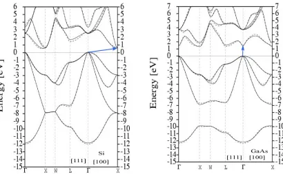
allowed energy states versus the propagation constant, k→ , gives a useful representation of the band structure. A complete E-k plot is a complex three dimensional surface and varies based on the difference in periodicity along various crystal directions. For convenience, E-k relationships are plotted in two dimensions for the crystal directions of interest. Crystal directions are indicated by regions between Γ, L, X, and W as shown in Figure 2.3 for Si and GaAs.
Parabolic bands of the following form are often used as approximate models near the conduction band minimum and valence band maximum.
* 2 2
2 ) (
o m
k k
E = h [ 2.4 ]
Effective mass, mo*, is similar to the mass of a free electron, mo, but accounts for the
electron or hole interaction with the periodic potential of the lattice. Values for effective mass are normally given as a fraction of mo which can be greater than or less than 1. Since
the parabolic curvature is usually different for the valance and conduction bands in a given material, the effective mass must also be different. Hole effective mass, mh*, is typically
larger than electron effective mass, me*, which is consistent with the curvature difference
respectively. Effective mass is a very useful parameter for band related mathematical modeling.
Figure 2.5 Energy Band Structure of Si and GaAs (After Chelikowski38 and Cerdá39) Arrows Indicate Indirect Transition in Si and Direct Transition in GaAs
The band structure reveals the fundamental reason that Si has low optical photon absorption and is an inferior material for solar cells. Consider an electron jumping from the top of the valence band to the bottom of the conduction band, indicated by the blue arrows.
absorption, will be discussed in the next section. Semiconductors are classified as either direct like GaAs or indirect like Si.
An important parameter that comes from band structure analysis is the Fermi level, EF. At absolute zero, electrons have no kinetic energy and fill the available energy states
lowest to highest until all available electrons are bound. The Fermi level is the top of this collection of electron energy levels and is symmetrically located between the filled and unfilled states, so all states below are filled and all state above are empty. Among other things, the Fermi level is a natural reference point for predicting the distribution of electrons over allowed energy levels given by the Fermi-Dirac distribution function.40,41
kT E E F e E
f ( )
1 1 )
( −
+
= [ 2.5 ]
As temperature increases, there is some probability that states below EF are empty and an
equal probability that states above EF are filled. The Fermi level lies in the bandgap of
semiconductors so it is important to understand that the Fermi-Dirac function is the probability that an electron will occupy an available state. No available states exist in the bandgap so there is zero probability of finding an electron there.
2.2.3 Electrons and Holes
treated as positively charge particles that can also conduct charge. In reality, electrons move in the valence band just as they do in the conduction band. However, it is convenient keep track of the relatively small number of holes that have the same dynamic as electrons except the charge is opposite so holes move the opposite direction of electrons in the presence of an electric field. Electrons move in the opposite direction of an applied field and holes move in the field direction.
CB
VB
T = 0K T > 0K
E
gElectron Hole
CB
VB
T = 0K T > 0K
E
gElectron Hole
Figure 2.6 Simplified Diagram of Valence and Conduction Bands, Bandgap, and Electron and Hole Behavior at Absolute Zero and Finite Temperatures
Thermal excitation of carriers across the bandgap is inadequate for the conduction necessary in most devices at reasonable temperatures. Two other methods of free carrier generation are crucial for many devices, including solar cells. When a semiconductor is exposed to light, photons with energy greater than Eg will be absorbed by electrons in the
semiconductor unabsorbed and therefore do not contribute to carrier generation. Only photons with energy approximately equal to or slightly higher than the bandgap promote electrons from the top of the valence band to the bottom of the conduction band. Higher energy photons create electron-hole pairs deep in the respective bands as shown. These electrons and holes quickly move back to the band edge by giving up the extra energy as heat to the lattice. This energy lost as heat, combined with unabsorbed lower energy photons, limits solar cell efficiency more than any other parameters. For indirect material, the probability of a low-momentum photon promoting an electron to the CB is relatively low. This is the fundamental limitation of Si, or other indirect semiconductors, as a PV material.
CB
VB
Electron
Hole
h
υ ≈
E
gh
υ
> E
gCB
VB
Electron
Hole
h
υ ≈
E
gh
υ
> E
gFigure 2.7 Photogeneration of Carriers
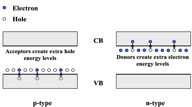
valance electrons than the host atoms, or acceptors, form energy levels just above the
valence band and are able to accept electrons from the valence band. Semiconductors doped in this manner are dubbed p-type because of the positively charged holes created in the valence band. Donor dopants having additional valence electrons compared to the host atoms form energy levels just below and donate extra electrons to the conduction band, creating an n-type semiconductor. Pure undoped, or intrinsic, semiconductor material has an equal number of electrons in the conduction band and holes in the valence band. Doped, or extrinsic, material has a much higher concentration of one type of carrier versus the other. This difference in p-type and n-type plays a critical role in many devices, including solar cells. The Fermi level shifts from mid-gap to an energy between the dopant level and the band edge at absolute zero temperature. Since the dopant energy levels are close to the band edges, only a small increase in temperature is required to activate transitions. At room temperature, essentially all these carriers will be ionized.
CB
VB
Electron
Hole
p-type
n-type
Donors create extra electron energy levels
Acceptors create extra hole energy levels
CB
VB
Electron
Hole
p-type
n-type
Donors create extra electron energy levels
Acceptors create extra hole energy levels
Figure 2.8 Acceptor dopants enhance conduction in p-type semiconductors via creating holes in the valence band. Donor dopants enhance conduction in n-type semiconductors via
A parameter of particular importance to solar cells is the carrier recombination lifetime. Electron-hole pairs created by absorption of photons remain in the excited state for a finite amount of time, usually on the order of nanoseconds. This is directly related to the diffusion length, or how far an electron or hole can travel through the material before being annihilated by recombination. For solar cells, the carriers need to remain in the excited state long enough to be collected and add to the output current. Poor material quality can
drastically reduce recombination lifetimes and will be addressed later in terms of specific materials systems.
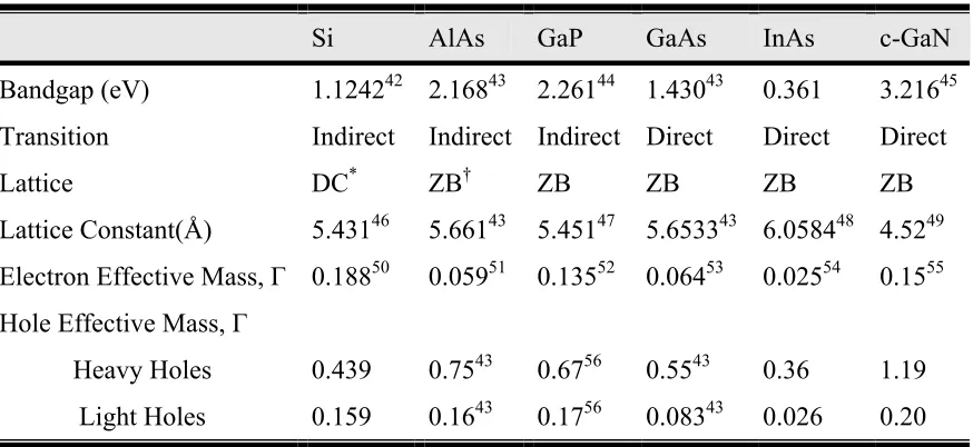
Several of the parameters discussed above are listed in Table 2.1 for GaAs and other photovoltaic binary alloys related to this work. Si is included for comparison. Properties of multinary alloys are frequently found by an appropriate approximation scheme using the binary values as endpoints.
Table 2.1 Selected Semiconductor Parameters
Si AlAs GaP GaAs InAs c-GaN
Bandgap (eV) 1.124242 2.16843 2.26144 1.43043 0.361 3.21645 Transition Indirect Indirect Indirect Direct Direct Direct
Lattice DC* ZB† ZB ZB ZB ZB
Lattice Constant(Å) 5.43146 5.66143 5.45147 5.653343 6.058448 4.5249 Electron Effective Mass, Γ 0.18850 0.05951 0.13552 0.06453 0.02554 0.1555 Hole Effective Mass, Γ
Heavy Holes 0.439 0.7543 0.6756 0.5543 0.36 1.19 Light Holes 0.159 0.1643 0.1756 0.08343 0.026 0.20 (values from Adachi57 unless otherwise noted)
2.2.4 Junctions
Photogeneration of carriers is the key phenomenon for solar cells, but a driving force to move the carriers is required to create the photovoltaic effect. Otherwise, carrier lifetime dictates that the carriers will simply recombine. This force comes from the interaction of p-type and n-p-type material at a junction. As mentioned previously, the Fermi level lies close to the band edge for doped semiconductors as shown in Figure 2.9. The valence and
conduction bands are represented by the energy levels at the top of the valence band, Ev, and
the bottom of the conduction band, Ec, respectively. Forming a junction produces several
Ec
p n p
-
+
nEF
EF
Ev Ev
Ec
Ec
EF
Ev
EA
ED
ED
EA
Ec
p n p
-
+
nEF
EF
Ev Ev
Ec
Ec
EF
Ev
EA
ED
ED
EA
Figure 2.9 p-n Junction Formation and Resulting Band Structure
For solar cells, excess carriers are generated from incoming photons. The built-in field of the junction separates the carriers by sweeping holes and electrons in opposite directions. Photovoltage is produced for an open circuit, VOC, and photocurrent is produced
for a short circuit, ISC. Along with photogeneration of carriers, this phenomenon is critical
for the photovoltaic effect.
2.3 DEVICE PRINCIPLES
For an electrical circuit, a solar cell is similar to a battery in that it delivers DC power to a load. Of course batteries produce a constant voltage from an electrochemical potential difference. Solar cells require illumination to produce the potential difference.
2.3.1 Photocurrent, Dark Current, and Photovoltage
Short circuit photocurrent density depends on the incident spectrum and the
quantum efficiency, QE(E), the probability that a photon with energy, E, will produce one electron for conduction. Defining F(E) as the incident flux where q is the electronic charge, the short circuit current density is given by:
∫
=
q
F
E
QE
E
dE
J
SC(
)
(
)
[ 2.6 ]Quantum efficiency is a useful tool for characterizing solar cells under different conditions because it depends on the absorption characteristics and transport properties of the
semiconductor, but not on the incident spectrum.
Current-voltage (I-V) or current density-voltage (J-V) characteristics of the pn-junction described in section 2.2.4 are useful for describing dark and illuminated behavior and several key parameters for solar cells. Diodes pass very little current under reverse bias because the bands shift to increase the potential barrier at the junction. A forward bias reduces the barrier allowing large currents once the applied voltage overcomes the barrier. This rectifying behavior is a consequence of the asymmetric junction required for charge separation and can be seen in the J-V plot, Figure 2.10.
Voltage, V
C
u
rr
en
t D
en
si
ty
, J
VO C
JS C
Light Current Dark Current
Dark current and light current represent the current passed under bias for a diode in the dark and an illuminated diode, respectively. The light current curve passes through the third quadrant where power is produced. For a solar cell connected to a load, a potential difference is established between the terminals resulting in a current opposing and reducing the photocurrent. While this current is not necessarily equal to the dark current, it is a good approximation for many solar cells and the dark current density can be easily calculated for an ideal diode by the Shockley diode equation.58
⎟
⎠
⎞
⎜
⎝
⎛
−
=
1
)
(
0 kTqV
Dark
V
J
e
J
[ 2.7 ]J0 is a constant, k is Boltzmann’s constant, and T is temperature in Kelvin. Net current
density for an ideal diode is a sum of the photocurrent, JSC, and the dark current, JDark, where
JSC is designated as positive.
⎟
⎠
⎞
⎜
⎝
⎛
−
−
=
1
)
(
0 kTqV
SC
J
e
J
V
J
[ 2.8 ]Many factors in real solar cells may limit the net current, so and ideality factor, n, is used to modify the equation above to reflect actual performance.
⎟
⎠
⎞
⎜
⎝
⎛
−
−
=
1
)
(
0 nkTqV
SC
J
e
J
V
J
[ 2.9 ]When the dark current equals the photocurrent, the net current is zero. This is analogous to an open circuit where voltage is at a maximum, VOC. Solving the equation
⎟⎟ ⎠ ⎞ ⎜⎜ ⎝ ⎛ +
= ln 1
0 J J q kT V SC
OC [ 2.10 ]
Notice in Figure 2.10, the current-voltage product is negative from 0V to VOC. This
is the range where solar cells are operated and produce power. For V > VOC, power is
consumed and photons are emitted which is characteristic of another important
optoelectronic device, the light emitting diode (LED). Photodetectors operate in the regime where V < 0.
2.3.2 Fill Factor and Efficiency
Maximum power output for a solar cell occurs at some point along the J-V curve where the current-voltage product is maximized. A power rectangle can be drawn by connecting this point to the axes as shown in Figure 2.11. Comparing this area to the light current curve yields the fill factor, FF.
SC OC m m
J
V
J
V
FF
=
[ 2.11 ]Ideally, the FF will cover as much area as possible under the J-V curve.
V
J
Fill Factor
JS C
Jm
VO C
Vm
M ax Power Point
For real cells, power is lost via the series resistance and leakage currents along defects or the sides of the device. The fill factor reveals these performance limiting parameters. In an equivalent circuit, these can be represented as two parasitic resistances. Series resistance, RS, is a concern for the metal contacts and should be as low as possible,
especially when concentrators are used to give a high current density. Resistance for any parallel or shunt leakage currents, RSh, should be as high as possible. Figure 2.12
demonstrates the effect on J-V curves of a decreased RSh and an increased RS. In both cases,
the maximum power point is shifted such that FF is reduced.
RS
RSh
IPhoton IDark
RS
RSh
V J Decreasing RSh
V J
V J Decreasin
Increasing RS
IPhoton IDark g RSh
V J Increasing R
S
Figure 2.12 Equivalent Circuit & Parasitic Resistances
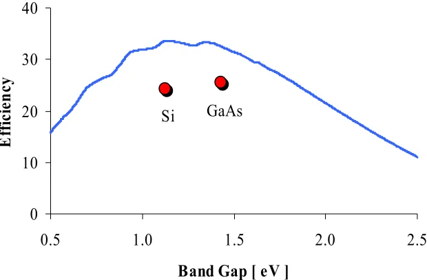
Most modern photovoltaic research and development, including this work, focuses on increasing output power via some scheme that increases efficiency. Efficiency is a ratio of the power density at Vm and Jm to the incident power, Pi. The fill factor allows efficiency
to be calculated in terms of VOC and JSC. Clearly, any reduction in fill factor, as in Figure
i SC OC
i m m
P FF J V P
J V
= =
η
[ 2.12 ]For a fixed incident spectrum, the relations presented in this chapter can be solved to predict the maximum possible efficiency based on bandgap alone. The detailed-balance approach proposed by Shockley59 provides a more rigorous and general prediction of maximum thermodynamic efficiency. A general numerical computer model, consistent with detailed-balance assumptions, has been developed to accurately predict the maximum efficiency dependence on bandgap for given spectra. Radiative recombination is the only loss mechanism included in the model as other loss mechanisms depend on specific device parameters. A model for a particular device would include the effects of series resistance, material quality, device structure, etc. Therefore, the detailed-balance efficiency should be perceived as a starting point from which the efficiency degradation from each loss
0 10 20 30 40
0.5 1.0 1.5 2.0 2.5
Band Gap [ eV ]
E
ff
ici
en
cy
Si GaAs
Figure 2.13 Limiting Efficiency for Single Junction Solar Cell. Verified Record Efficiency for GaAs and Si Indicated in Red
2.3.3 Cell Design Considerations
Optimizing a solar cell design is an exercise in compromise as many of the requirements are conflicting. For the top metallic contact, the coverage should be
minimized to avoid blocking incident photons which indicates contacting only the sides of the layer. In contrast, the diffusion lengths of carriers are too short to be collected by side contacts. As a consequence, thin metallic fingers are spread across the surface and
connected via a bus bar as in Figure 2.14 or some similar approach. The fingers must be spaced within the carrier diffusion length and should be thin to avoid shading, but not so thin that series resistance is increased.
indicated for the n-layer, the p-layer can be lightly doped to improve carrier collection without sacrificing VOC. Clearly, the depletion region must extend further into the lightly
doped region to reach equilibrium.
High quality semiconductor surfaces are fairly reflective such that more than 30% of the incident power can be lost before any interaction with the junction is possible.
Therefore, essentially every modern solar cell has an anti-reflective(AR) coating with an index of refraction between the index of the semiconductor and air. AR coatings are optimized to channel the preferred photons into the semiconductor.
Junctions should be near the surface. Otherwise, carriers generated in material above the junction will be lost to recombination before they can be collected. Simultaneously, the total junction thickness should be greater than the absorption length. We have assumed to this point that any thickness will absorb all electrons with energy greater than Eg, but this is
incorrect. For a photon to be absorbed, it must have an opportunity to interact with an electron in the correct energy and momentum state for excitation across Eg. This may not
Back Contact Top Contact n-type
p-type AR Coating Transparent Adhesive Cover Glass
Back Contact Top Contact n-type
p-type AR Coating Transparent Adhesive Cover Glass
Figure 2.14 Typical Solar Cell Design
3 MULTI-JUNCTION SOLAR CELLS
Since a single photovoltaic junction has a rather low limit of efficiency, an obvious solution is to use multiple junctions to absorb different parts of the spectrum. Each
individual junction can then be illuminated with photons of energy close to the bandgap. Efficiency increases in each junction and can be combined into a greater overall efficiency by electrically connecting them in series or parallel. The concept was proposed as early as 1955,61 but technology at the time was inadequate to develop useful devices. Several schemes have since been developed and each has certain benefits and detriments.
Dichroic mirrors selectively reflect light based on wavelength and can be used to split the spectrum onto different junctions.62 Efficiency gains have been realized by this method,63 but there are several factors that make this approach cumbersome. Processing, packaging, mechanical support, electrical connections, power conditioning devices, and labor are increased by a factor equal to the number of junctions making production costs a serious concern. Also, the dichroic mirrors are responsible for a small amount of loss and must be specialized for each junction. Typically, junctions used in this manner are
connected in parallel which allows individual control of each and overall current is increased. Increased current can be useful, but also suffers from series resistance losses.
A more clever solution is to stack the junctions, using the top junction as a filter to collect high energy photons and transmit lower energy photons to the next junction. In the literature, this scheme may be referred to as a cascade, tandem, or multijunction solar cell. Mechanical stacking of junctions has also been developed64,65,66 and has similar benefits and
electrically contacted in parallel. Mechanical stacking can result in bulky end products and high production costs.
More promising than these two methods are monolithic stacked cells where the junctions are directly connected in optical and electrical series. First realized by Bedair, et. al67,68 in a 2-junction device, this approach has been successfully developed by many for several materials systems. (See Figure 1.1) Initially, connecting junctions in series was problematic because stacking two pn-junctions results in reversed third junction between the two middle layers. However, this issue has essentially been solved via tunnel junction technology.69,70 Tunnel junctions are heavily doped p+/n+ regions that essentially form an ohmic contact between solar cell junctions. Perhaps the most fundamental limiting factor with this design is the requirement that each junction produce the same current. However, current matching can be achieved and this design is an elegant stack of junctions that double as optical high-pass wavelength filters. Electrical series connection increases voltage and decreases current compared to a single junction. This is fortunate in terms of limiting the detriment of series resistance and producing emf for useful work. This device only requires two terminals and is contacted similar to a single junction.
3.1 LATTICE MATCHING
Recall from section 2.2.1 that a crystalline material has a characteristic lattice
problem for multijunction solar cells because overlying junctions with ideal bandgaps may not have the same lattice parameter as the underlying substrate. Consequently, lattice misfit dislocations can form which aid in non-radiative recombination of carriers, causing poor efficiency. Consider a layer of crystalline material formed on a crystalline substrate with a different lattice parameter. If the layer is relatively thin, the lattice mismatch strain will be accommodated elastically by stretching the atomic bonds at the interface. Strain increases with layer thickness until, at some critical thickness, misfit dislocations form to
accommodate the strain.
Strained Top Layer
Strain Partially Relieved via Misfit Dislocation Formation Strained Top Layer
Strain Partially Relieved via Misfit Dislocation Formation
Figure 3.1 Lattice Mismatch Strain Relaxation via Formation of Dislocations
Two well known models have been presented to predict this critical layer thickness, hc. The Matthews-Blakeslee model71 considers an equilibrium situation where the sum of
strain and dislocation energy is minimized to give the following relation:
(
)
(
)
⎥⎦ ⎤ ⎢ ⎣ ⎡ + ⎟ ⎠ ⎞ ⎜ ⎝ ⎛ − −= ln 1
cos 1 4 cos 1 2 b h f b h c
c
π
ν
λ
θ
ν
where b is the Burger’s vector, υ is Poisson’s ratio, and f is the misfit parameter. The model presented by People and Bean assumes an energy barrier exists to the formation of a
dislocation such that the strain energy is equal to the dislocation energy, resulting in
(
)
(
)
⎢
⎣
⎡
⎟
⎠
⎥
⎦
⎤
⎞
⎜
⎝
⎛
+
−
=
b
h
f
b
h
c cln
1
32
1
2ν
π
ν
. [ 3.2 ]
Neither model fully describes experimental data and there is considerable debate as to why each one seems to fit certain situations. Several others have contributed both commentary and alternative models72,73 to the general explanation of this phenomenon. Jain, et al74 have assembled a thorough review of the topic with valuable discussion of the validity of various models. The critical layer thickness dependence on lattice mismatch is plotted in Figure 3.2 for both popular models. Matthews-Blakeslee is considerably more conservative and will be used in this work as a safe approximation.
1 10 100 1000 10000
0 0.5 1 1.5 2 2.5 3
M ismatch Parameter, M [ % ]
C ri tic al T h ic k n es s [ Å ]
People & Bean
Matthews & Blakeslee
3.2 MATERIALS FOR MULTIJUNCTION PHOTOVOLTAICS
Theoretically, the number of possible junctions has been analyzed up to the limit of infinite junctions.75 In practice, two-junction (2J) cells have been developed76,77 and are commercially available78. 3J cells are still being developed79,80 and are available for specialized space applications.78,81 3J cells also claim the current world record efficiency60 and may have potential for the terrestrial market.17 4, 5, and 6J cells have been proposed and some preliminary laboratory data can be found in the literature,82 but not with any record efficiencies. The limiting efficiency model presented in Section 2.3.2 can be applied to multiple junctions to aid in material selection.
3.2.1 Candidate PV Semiconductors for High Efficiency
Top Cell Bandgap [ eV ]
1.0 1.2 1.4 1.6 1.8 2.0
B
ottom
Cel
l Ban
d
gap
[ eV ]
0.6 0.8 1.0 1.2 1.4
28 30 32 34 36 38 40 42 44 46
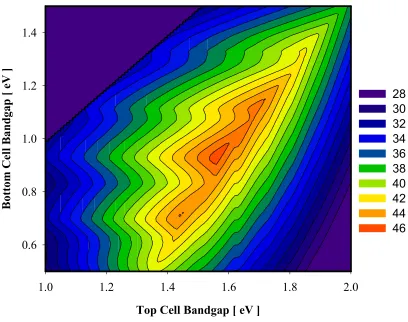
Figure 3.3 AM1.5D 2-J Cell Thermodynamic Limiting Efficiency Contours (Maximum at 1.56eV and 0.93 eV)
system for photovoltaic applications. Alloying InN with GaN(3.4eV) covers a very wide range of the solar spectrum, but the technology is still in it’s infancy. Alloys of
III-Arsenides, III-Phosphides, and III-Antimonides range from around 0.4eV to 2.5eV, covering a large part of the solar spectrum. Figure 3.4 shows the bandgap dependence on lattice parameter for several important materials. The relationship for ternary alloys is usually non-linear so a bowing parameter,87 b, is adapted to the linear relationship to account for the
curvature seen in the blue lines connecting binary compounds. Seemingly, we can now just pick the appropriate materials from Figure 3.4 and form a high efficiency solar cell.
However, not every composition of alloy can be formed with adequate quality. Coupling this with lattice matching and bandgap requirements, the number of available materials is rather limited.
GaAs
InAs
GaP AlAs
InP Si
Ge
0 1 2
5.4 5.5 5.6 5.7 5.8 5.9 6 6.1 6.2
Lattice Constant [ Å ]
B
an
d
gap
[
e
V
]
3.2.2 Survey of Developed PV Materials Systems
Early work focused on using GaAs substrates as the bottom junction in part due to high-quality commercial availability and previous development for photovoltaics. The highest quality and least expensive substrates are Si, but it is clear from Figure 3.4 that none of the potential top cell materials can be lattice matched to Si. From inspection of Figure 3.3, if GaAs(1.42eV) is the bottom cell, it should be coupled with a top cell of around 1.9eV to yield the best efficiency. Two promising ternary alloys, lattice matched to GaAs, meet this requirement; Al0.4Ga0.6As and Ga0.5In0.5P. AlGaAs was used initially with promising
results, but several problems, including oxygen contamination in the layers, caused inconsistent performance.88 GaInP was developed89 and has seen extensive use
commercially. The record efficiency for this 2J arrangement steadily increased to 30.3%,90 reported in 1996.
Widely available, high quality Ge substrates led researchers to utilize them in PV technology. From Figure 3.4, the lattice spacing of Ge is nearly equal to GaAs, so it can be substituted for GaAs in an existing technology with very little mismatch. Compared to GaAs, Ge has higher strength and is less expensive, but has an indirect bandgap of 0.67eV. Nearly lattice matched 2J GaAs/Ge solar cells are well developed91 and widely used in space applications92 with efficiency around 20%. GaInP/GaAs 2J cells have also been produced on Ge substrates for space applications with efficiencies around 23%.93
seek a solution for the other major loss mechanism, transparency to low energy photons. A third lattice matched junction with a bandgap lower than GaAs, inserted below the
GaInP/GaAs stack, could absorb some of the low energy photons and increase efficiency. Applying the efficiency model with the middle cell set to the bandgap of GaAs, again yields an optimum top cell bandgap around 1.9eV. For the bottom cell, a bandgap around 1eV is indicated as shown in Figure 3.5. Unfortunately, a high quality material with a bandgap of 1eV that is lattice matched to GaAs does not exist in the range of commonly known photovoltaics.
Top Cell Bandgap [ eV ]
1.5 1.6 1.7 1.8 1.9 2.0 2.1 2.2
B
ottom
Ce
ll
B
and
gap
[ e
V
]
0.6 0.7 0.8 0.9 1.0 1.1 1.2 1.3
30 32 34 36 38 40 42 44 46 48 50
Figure 3.5 AM1.5D 3J Top and Bottom Cell Efficiency Contours with GaAs Middle Cell
substrate. NREL94 and Spectrolab, Inc.95 have led the development of GaInP/GaAs/Ge 3J
cells, trading record efficiencies for the past few years and have received prestigious awards for their efforts. Spectrolab narrowly holds the record at this time, as mentioned previously. The reason that Ge can be used successfully despite the indirect bandgap is because the junction is formed on the thick substrate. Low absorption coefficient requires many microns of Ge for complete photon absorption which is available in this case. A thin junction of Ge would be inadequate. The low bandgap of Ge results in excess current generation, so a fourth junction is considered between GaAs and Ge to share the photon flux. Applying the efficiency model to this 4J structure, (Figure 3.6) a bandgap near 1eV is predicted again, consistent with values found in the literature.96
Top Cell Bandgap [ eV ]
1.5 1.6 1.7 1.8 1.9 2.0 2.1 2.2
T
hi
rd Cell
B
an
dgap [
eV
]
0.6 0.7 0.8 0.9 1.0 1.1 1.2 1.3
34 36 38 40 42 44 46 48 50 52 54
Without a suitable 1eV material, this established GaInP/GaAs technology is simply unable to make further large gains in efficiency. Some efficiency can be gained by adjusting the composition of the top two junctions to achieve an exact lattice match to Ge, and by tweaking the properties of each layer. Many other high efficiency multijunction
arrangements can be envisioned and, in fact, have been proposed by several researchers for a variety of materials. However, none have yet proven to be commercially viable and it is not the intent of the author to detail each possibility. A viable 1eV junction could be quickly integrated into existing technology with significant efficiency gains, but which material(s) will satisfy this requirement?
3.2.3 Pursuit of a 1eV Lattice Matched PV Junction
The prospect of a viable 1eV junction for PV applications was grim until the mid-1990’s when a relatively unknown material system was introduced. Weyers et al.97 first reported optical properties of dilute GaAsN in 1992.97 A strong apparent reduction of the bandgap is reported compared to GaAs, around 100meV for only 0.5% N.98 Soon after, in 1994, Kondow et al. proposed GaAsN as a Si lattice matched material for light emitting diodes and noted a large bowing parameter.99 Then in 1996, InGaAsN was proposed for laser diodes for the important fiber optic communications wavelengths, 1.3 and 1.5μm.100 From this point, GaAsN and InGaAsN held the attention of the broader optoelectronic community with a variety of possible applications. InxGa1-xAs1-yNy can have a bandgap of
two journals to devote an entire issue (Journal of Physics: Condensed Matter 16, 2004 and Semiconductor Science and Technology 17, 2002) to reviewing dilute nitrides. Henini also published a very thorough text on the topic in 2005.101
The literature is replete with reports of numerous defects and poor material quality, especially for N compositions greater than 1%. Our investigation into the growth of dilute nitrides (details reported in Chapter 8) resulted in generally poor crystalline, optical, and electrical properties with increased N composition. With respect to solar cells and other minority carrier devices, low carrier lifetime reduces performance to unacceptable levels. For the GaAs lattice matched, 1eV In0.08Ga0.92As0.97N0.03 layer primarily considered for a
third junction, it has been demonstrated that the carrier diffusion length is less than the depletion width for material of typical to high quality.102 Additional reports on this alloy
indicate poor quantum efficiency, diffusion lengths, carrier lifetime, photocurrent, and open circuit voltage.103,104,105,106 Significant work has been done to isolate the specific defect(s) that result in low minority carrier lifetime. Many defects have been identified and ruled out as the primary cause. One suspicious defect has been measured by deep level transient spectroscopy (DLTS) and is the most likely culprit, but the particular defect remains unknown.107,108
Despite these troubles, adequate device performance has been demonstrated to justify continued development, especially considering the potential gains if material quality is mastered. Typical parameter values for InGaAsN solar cells grown by OMVPE are VOC =
0.3V, ISC = 2mA/cm2, and FF = 60%.103 The best reported values are from p-i-n junctions
grown by MBE with values of VOC = 0.45V, 9.5mA/cm2, and FF = 64%.109 Expected open
low short circuit is most concerning as ~17mA/cm2 is required110 for current matching in a
3J GaInP/GaAs/InGaAsN cell. If ISC can be improved or if the required current can be
4 PROPOSED NOVEL THIRD JUNCTION
If thick 1eV layers of dilute nitrides are inherently defective and thick layers of other III-V materials can not be lattice matched to GaAs, more complex structures can be
considered. InxGa1-xAs is known to be of excellent quality in the absence of large misfit
strain induced dislocations. Lattice matching to InP substrates occurs for x = 0.48, and this combination has been successfully demonstrated for waveguides,111 single photon avalanche
diodes(SPAD),112 heterojunction bipolar transistors(HBT),113 high electron mobility transistors(HEMT),114 and several other devices. For x = 0.3, the bandgap is around 1eV and from experience with InGaAs, this composition can be attained with OMVPE with high quality. To take advantage of the high material quality of InGaAs for solar cells, the issue of lattice mismatch must be addressed.
4.1 STRAINED LAYER SUPERLATTICES
Strained layer superlattices(SLS) offer a way to avoid generation of misfit
dislocations by taking advantage of the critical layer thickness, hc, discussed in section 3.1.
For example, InGaAs can be grown without misfit dislocations on GaAs with a film
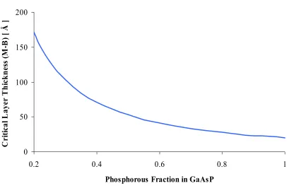
thickness less than hc. However, for any useful In compositions, the critical layer thickness
is relatively low, only 43Å at 30% In according to the Matthews-Blakeslee model. This very thin layer is not adequate to absorb a high percentage of photons due to the absorption coefficient. InGaAs is compressively strained to GaAs, so a second layer of tensile strained material can be grown on top of the InGaAs. This layer should have equal but opposite strain and should also remain below hc. Strain is thereby balanced and the average lattice