A
BSTRACT
Carroll, Richard Lloyd. Studies of the Structural and Electronic Properties of Self-Assembled Monolayers – Towards Molecular Electronics (Under the direction of
Professor Christopher B. Gorman)
The field of Molecular Electronics (ME) is growing at a rapid pace. The study of
materials that have utility at the level of several, or single, molecules is exciting because
the development of these sorts of systems offers a pathway to potentially avoid the perils
of continually shrinking Silicon-based fabrication. This work examines the state of the art
in fabrication techniques for semiconductor systems, then examines current examples of
ME to be found in the academic literature. This review is designed to plumb the depths of
a few important demonstrations, as opposed to a broad overview of the entire body of
work. Further, scanning probe lithography techniques are demonstrated that allow for the
study of small ensembles of interesting molecules in isolation. By utilizing these
techniques, the structural and electronic properties of molecules can be studied, with a
focus towards determining the likely utility of a particular species in a ME framework.
Experimental study of redox-active self-assembled monolayer (SAM) films shows that
under specific conditions, some films display a negative differential resistance (NDR)
response that has possible utility in the development of ME devices. Ferrocene- and
galvinol-terminated SAMs both show NDR at room temperature. A possible mechanism
for the NDR behavior is believed to be resonant tunneling through low-lying, accessible
Richard Lloyd Carroll was born March 24, 1969, to Richard E. and Carolyn T.
Carroll. An Army brat for the first twelve years of his life, he, his mother, and two
younger brothers returned to the rural metropolis of Roxboro, NC in the early 80’s. After
graduating from Person Senior High School in 1987, he attended North Carolina State
University as a North Carolina Teaching Fellow. While in attendance he met his
soulmate, Marcia Walsh. Graduating in 1991 with his B. S. in Secondary Education, he
obtained a position on the faculty of Northern Vance Senior High School in Henderson,
NC as a Biology, Chemistry, and Physical Science Teacher. Soon thereafter, he and
Marcie married. Through interactions with members of the teaching faculty in Physics
and Chemistry at NC State, he grew interested in the prospect of graduate education. In
1995, after completing three-and-a-half years of teaching, he entered NC State as a
post-baccalaureate student. In 1996, he began his pursuit of the Doctor of Philosophy degree
A
CKNOWLEDGEMENTS
I would be remiss if I did not immediately give great thanks and much appreciation
to my advisor and mentor, Prof. Christopher B. Gorman. While we don’t agree on
everything, Chris has done me a great service over the past several years in letting me
make my own mistakes, then helping me to understand how not to make them again.
I gratefully acknowledge all of the past and present members of the Veal Hut, for
without them, I would have had a much longer and decidedly less interesting graduate
career. I especially want to thank Ryan Fuierer for making it easy to teach him the ropes,
so that I could have a colleague, as opposed to a burden.
Drs. Yufan He and Fang Tian were very helpful in their time with us, and I heartily
thank them for their input and assistance.
Thanks to all the other members of the Gorman Group, past and present. We are an
eclectic bunch, and a lot of fun.
I thank Professor David Shultz for supplying our group with
phenoxygalvinol-terminated thioacetate, Russell Miller for ferrocene-phenoxygalvinol-terminated thioacetate and Professor
Younan Xia for the microcontact printing stamp. I would also like to thank Professor
Robert Birge for preprints of theoretical work.
Finally, I have to thank my wife, Marcie, my daughter, Callie Marie, and my son,
Jackson Lloyd for putting up with Daddy’s long, sleepless nights, and for being there
with love and encouragement. While I might enjoy it a little more than you do, all of this
T
ABLE OF
C
ONTENTS
L
IST OFF
IGURES...vii
L
IST OFT
ABLES...xiii
C
HAPTER1 - T
HEG
ENESISO
FM
OLECULARE
LECTRONICS...1
1.1. Conventional Electronics and its Boundaries ...2
1.1.1. Transistor Development and Moore’s Law ... 2
1.1.2. Conventional Techniques – Limitations and Outlook ... 4
1.1.3. Definition of Molecular Electronics... 8
1.2. Molecular Device Efforts in the Literature...10
1.2.1. Historical Beginnings – Molecular Rectifiers ... 10
1.2.2. Wiring Up – Molecular Wires ... 18
1.2.3. Static Elements – Data Storage ... 25
1.2.4. Transistorized – Molecular Switches ... 30
1.2.5. Special Cases – Negative Differential Resistance... 42
1.2.6. Closing Thoughts... 45
1.3. References...46
CHAPTER 2 - T
HEI
NFLUENCEO
FH
EADG
ROUPO
NT
HES
TRUCTUREO
FS
ELF-A
SSEMBLEDM
ONOLAYERS...50
2.1. Introduction...51
2.2. Results and Discussion ...52
2.2.1. Alkene-terminated thiol displays hexagonal and superlattice adlayers ... 52
2.2.2. Cyano-terminated thiol displays both single-row and double-row adlayers ... 53
2.2.3. Carboxylic acid-terminated thiol displays double-row adlayers ... 55
2.3. Conclusions ...58
2.4. References...59
C
HAPTER3 - R
EPLACEMENTL
ITHOGRAPHY...62
3.1. Introduction...63
3.2. Results and Discussion ...64
3.2.1. Procedure... 64
3.2.2. Apparent Height ... 65
3.2.3. Mechanism and Humidity... 67
3.2.4. Resolution... 69
3.2.5. Multi-Thiol Replacement... 70
3.2. Conclusions ...71
3.3. Experimental Details ...71
C
HAPTER4 - N
EGATIVED
IFFERENTIALR
ESISTANCEI
NP
ATTERNED, E
LECTROACTIVES
ELF-A
SSEMBLEDM
ONOLAYERS...74
4.1. Introduction...75
4.2. Results and Discussion ...76
4.3. Conclusions ...86
4.4. Experimental Details ...86
4.5. References...91
APPENDIX 1 - M
ACROSF
ORA
NALYSISO
FCITS D
ATAI
NK
ALEIDAGRAPH...94
A1.1. Reject aberrant curves ...94
A1.2. Mask Central (Noisy) section of data...96
A1.3. Make a Voltage Column with Sequential Voltage values ... 98
A1.4. 5-point derivative , modified by magnitude of curve ...98
A1.5. Offset Central region to voltage 0... 100
A1.6. Peak Separation Finder ... 101
A1.7. Peak Finder ... 104
L
IST OF
F
IGURES
CHAPTER 1
Figure 1.1 - Point-Contact Transistor A) The original device, 1947; B) With no bias on the gate, there is no passage of current; C) When a signal is applied to the gate, it depletes the region under the tip, producing a p-n junction and allowing the flow of enhanced current ...2
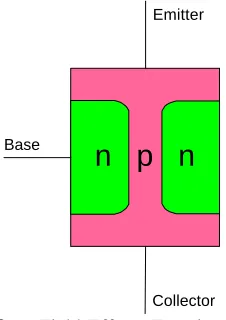
Figure 1.2 - Junction Transistor: A small current (or signal) between the Emitter and Base allows a much larger current flow from Emitter to Collector...3
Figure 1.3 - Field-Effect Transistor: Current applied to Base controls carrier density in conduction channel, and thus controls current between Emitter and Collector ...3
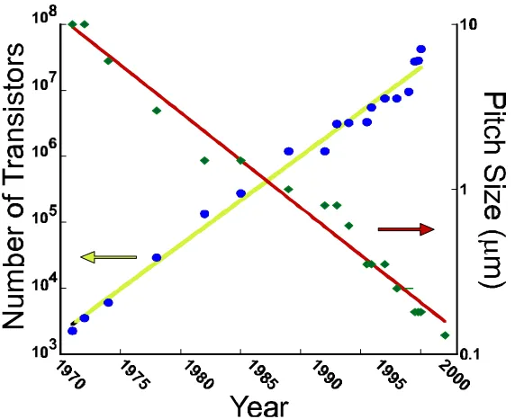
Figure 1.4 - Plot illustrating Moore's Law, applied to total number of transistors and minimum feature size...4
Figure 1.5 - Integrated Circuit Fabrication - The figure outlines the basic steps to fabricate a Junction FET. The process begins with an ultra-pure Si wafer. The Si is oxidized, then the oxide patterned by photolithography. The resulting pattern is developed, etched, then any remaining photoresist is stripped. The patterned oxide protects part of the surface during the implantation step, when dopants are added to certain regions of the surface. Using photolithography and Chemical Vapor Deposition, a polysilicon gate is deposited atop a thin gate oxide. Further layers of oxide are added to separate components and to protect others. Vias are etched through the oxides to allow contact to active regions. Interconnects are deposited - Al is evaporated, Cu is electrolytically deposited. Further oxides protect one layer from the layer of interconnections above. Finally, the surface is polished by CMP to prepare it for the next layer of interconnects and components...5
Figure 1.6 - Calculated I-V Curve for Molecule 1...12
Figure 1.7 - Energy level diagrams of molecule 1. A) The donor-acceptor system between two metal electrodes; B) Positive applied bias; C) Reverse applied bias ....12
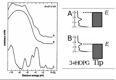
Figure 1.8 - UPS spectra for A) acidified HOPG with bound 3; B) acidified HOPG; C) difference between a and b...14
Figure 1.9 - DOS of Molecule 3 and HOPG compared to EF of Tip, at A) 0 V applied
bias, and B) ~-1.3 V substrate bias ...14
Figure 1.11 - I-V curves from two different LB film configurations: A)"Ga/In eutectic|Al(100nm)|1 LB monolayer of 4|Al(100nm)|Ga/In eutectic"; B)"Ga/In eutectic|Al(100nm)|4 LB monolayers of 4|Al(100nm)|Ga/In eutectic" ...16
Figure 1.12 - Comparison of A) Aviram-Ratner model for neutral D-σ-A species, and B) modified model for zwitterionic D+-π-A- species ...17
Figure 1.13 - The relationship between proconductor and conductor. A) Conversion of proconductor (polythiophene) to conductor (polythiophenium) by oxidation; B) Simplified energy level diagrams for the proconductor and conductor between two metal electrodes ...18
Figure 1.14 - A) CVs of three polyynediyl species, 10-5 M in 0.1 M Bu4N+BF4
-/CH2Cl2
at 22.5±1 °C, Pt working and counter electrodes, potential vs Ag wire pseudo-reference, scan rate = 100 mV/s, ferrocene = 0.46 V; B) Plot of CV results for series from ReC2Re to ReC10Re, E1 is first oxidation, E2 is second oxidation, Ep,c and Ep,a
are cathodic and anodic peak potentials, respectively ...19
Figure 1.15 - A) Schematic illustration of the insertion of 9' into a disordered domain boundary of DT SAM. The dashed line represents the feature as imaged by the STM tip; B) Constant current STM image of 9' in molecularly resolved DT SAM. The bright spots of similar shape and size are the molecules of 9'...21
Figure 1.16 - ASV of copper on A) Au electrode with DT SAM, B) Au electrode with 10
SAM ...22
Figure 1.17 - ASV of vapor-deposited Cu on A) DT SAM, and B) SAM of 10. Triangles are first scan, dashes are second scan. "A" indicates the position at which potential sweep was stopped and the sample imaged by SEM...23
Figure 1.18 - Suspended crossbar configuration of proposed nonvolatile RAM. The figure shows a 3D view of four junctions in the proposed architecture, with two crossbar devices in ON state (in-contact) and two in OFF state (separated). The upper nanotubes are supported on organic or inorganic supports (grey blocks), while the lower nanotubes are directly in contact with insulating substrate (SiO2 - white) on conducting layer (highly doped Si - dark grey). The yellow blocks represent the electrodes used to address each nanotube ...26
Figure 1.19 - Configuration of "bucky-shuttle" memory elements A) Top view showing an array of "bucky-shuttles" and the crossed electrodes used to address them; B) Side view showing the elements addressed by electrode C in the Top View. By applying a reading or writing pulse between electrodes C and b, a specific element may be queried or written...27
Figure 1.20 - A) CV of 11a (25 µm diam. Au electrode, in electrolyte solution of 0.10 M
Bu4N+PF6
trace for reconnection of CE at OCP for neutral and oxidized 11b SAMs; C) Current trace for two Au electrodes (diam 25 and 10 µm) with 11b SAM, oxidized at +800 mV (vs. Ag/Ag+), disconnected for several seconds, then reconnected at the OCP
(+125 mV vs. Ag/Ag+) ...29
Figure 1.21 - Nanotube Field-Effect Transistor (TUBEFET). A) Schematic of device configuration; B) Band diagram for device. The nanotube EF is pinned at the EF of the metal electrodes where they are in contact. C) I/V curves at varying Vgate for the device. Inset: Conductance (G) at Vbias = 0 for varied Vgate...31
Figure 1.22 - Schematic of in-plane single-electron transistor. ~30 nm separates the source, drain, and gate electrodes ...32
Figure 1.23 - A) Plot of I/V curves collected between a source and drain electrode connected by a chain of three Au colloidal particles. The curves were collected at the temperatures indicated, with Vgate = 0; B) Plot of I/V curves collected as Vgate is varied from +0.4 V to -0.4 V. The curves are offset from each other for clarity; C) Plot of I/Vgate (or conductance) at various source-drain biases (VSD) ...33
Figure 1.24 - A) Schematic of self-assembled nanostructure, composed of xylyldithiol on Au(111) substrate, and the circuit diagram that describes the system; B) Plot of I/V curves collected at varied setpoint currents...34
Figure 1.25 - A) Schematic circuit of single molecule electromechanical amplifier based on interactgion of STM tip with C60 molecule; B) Plot of Vin (dashed line) applied to piezoelectric tube and resulting Vout (solid line) ...35
Figure 1.26 - LT-STM images of 13 on Cu(211) showing A) all arms in OFF position (nearly flat on surface); and B) one arm in ON position (oriented 55º out of plane of porphyrin); C) Turning ON arm OFF: Plot of current as the tip is moved from z = 7.5 Å towards surface. Dot on inset picture indicates tip position over ON arm...37
Figure 1.27 - Schematic representation of a proposed Atomic Relay Transistor ...38
Figure 1.28 - Schematic representation of molecular shuttle ...39
Figure 1.29 - Schematic representation of pseudorotaxane-based logic operation...40
Figure 1.30 - Graph of an I/V curve of 14 collected at 60 K...42
Figure 1.31 - Graph of I/V curve collected by STM over a monolayer of 17. Setpoint Bias was -5.0 V, and tunneling current varied from 3.05 to 30.5 nA ...43
CHAPTER 2
Figure 2.1 - STM images taken in low humidity air of a SAM composed from undec-10-ene-1-thiol. Scan parameters: A) Set Point Voltage (Vset) = 1.0 V, Setpoint Current
(Iset) = 3.9 pA, Scan Rate = 3.6 Hz; B) Vset = 1.0 V, Iset = 5.8 pA, Scan Rate = 20.4
Hz. Inset is a Fourier Filter solely as a guide to the eye; C) Vset = 1.2 V, Iset = 7.4 pA,
Scan Rate = 2.3 Hz. ...52
Figure 2.2 - STM images taken in low humidity air of a SAM composed of 10-cyanodecanethiol. Scan parameters: A) Vset = 1.0 V, Iset = 6.8 pA, Scan Rate = 1.9
Hz; B) Vset = 1.0 V, Iset = 6.6 pA, Scan Rate = 3.0 Hz. C) Vset = 1.0 V, Iset = 6.8 pA,
Scan Rate = 2.1 Hz; D) Vset = 1.0 V, Iset = 6.6 pA, Scan Rate = 1.9 Hz. Inset of panel
D is a Fourier Filter solely as a guide to the eye. ...54
Figure 2.3 - STM images taken under low humidity conditions of SAM composed of 11-mercaptoundecanoic acid. Scan parameters for all images are Vset = 1.0 V, Iset = 10.3
pA, Scan Rate = 2.3 Hz. ...56
Figure 2.4 - FFM images of a micro-contact printed SAM composed from dodecanethiol, 10-cyanodecanethiol and 11-mercaptoundecanoic acid as described in the text A) Before and B) After soaking for several hours in 0.1 M aqueous perchloric acid. ....57
Figure 2.5 - Reaction scheme illustrating the hydrolysis reaction from cyano- to amide, then further to the acid. ...57
CHAPTER 3
Figure 3.1 - Schematic of “Nanoshaving” - AFM-based replacement...63
Figure 3.2 - Schematic representation of the lithographic process of thiol replacement. A) Imaging at +1.0 V bias and ca. 10 pA setpoint current above the SAM. B) Replacement by increasing the setpoint bias to ca. +3.0 V. C) Imaging the replacement pattern...64
Figure 3.3 - STM images illustrating patterns of the letters NCSU in which A) dodecanethiol replaced decanethiolate (Vwrite = + 3.8 V, Vread = + 1.0 V, Iset = 6.0 pA,
ca. 60 % RH) and B) decanethiol replaced dodecanethiolate (Vwrite = + 3.6 V, Vread =
+ 1.0 V, Iset = 8.0 pA, ca. 60% RH). ...65
Figure 3.4 - STM images illustrating mixed SAMs prepared from decanethiol/dodecanethiol (10:1 molar ratio, vapor deposited) (A) imaged in air (Vset
= 1.0 V, Iset = 6.0 pA) and (B) imaged under dodecane (Vset = +1.0 V, Iset = 6.0 pA) ...
...66
under dodecane (Vset = +1.0V, Iset = 5.0 pA) B) sample removed from dodecane,
briefly rinsed in ethanol, dried and imaged (Vset = +1.0 V, Iset = 6.33 pA) ...67
Figure 3.6 - Schematic illustrating Reversed Apparent Height Contrast between SAMs in dodecane versus in vacuum/dry air. A) Resistance profile through films and gap (regardless of composition); B) Tip Height in vacuum/dry air. The dashed line indicates the tip path assuming it correctly tracked film height differences; C) Tip Height in dodecane. Actual height above the film is not known (indicated by wavy line). ...68
Figure 3.7 - STM image illustrating lines of decanethiolate SAM in a dodecanethiolate SAM background imaged under dodecane/decanethiol solution. The scale above shows the averaged height profile over the length of the lines. Replacement parameters were Vwrite = +3.7 V, 66 % RH. Imaging parameters were Vread = +1.0 V,
Iset = 6.0 pA...69
Figure 3.8 - Image showing writing with two different thiols on a dodecanethiolate SAM background. At the bottom of the image, decanethiolate SAM was written at Vwrite =
+3.2 V, Iset = 6.0 pA, 60 % RH. At the top of the image, hexadecanethiolate SAM
was written at Vwrite = +3.4 V, Iset = 6.0 pA, 60 % RH. Imaging parameters were Vset
= +1.0 V, Iset = 6.0 pA. ...70
CHAPTER 4
Figure 4.1 - A) Graph of a typical I-V curve collected from Fc-C11S-SAM under dodecane; B) Histogram representing position of NDR in Fc-C11S-SAM under dodecane...76
Figure 4.2 - Schematic model of NDR in Fc-C11-SAM. Panel A represents relative energy levels of the system at zero bias. Panels B-E represent changes in energy levels of the system as it is biased to arbitrary, positive potentials. The unfilled circle on each IVV curve represents the position on the curve for each potential. The arrow in each energy diagram represents the magnitude of current through the system...78
Figure 4.3 - Graph of representative I/V curves collected over FcC11S-SAM at different sweep rates ...79
Figure 4.4 - Schematic of scanning tunneling microscopy based lithography on SAMs. (A) Imaging above the SAM (1.0 V, 10 pA); (B) Replacement at increased bias (~3.0 V, 10 pA); C) Imaging of the replacement nano-structure (1.0 V, 10 pA)...80
Figure 4.5 - (A) STM image illustrating replacement of Fc-C11SH into a background of
C12S-SAM (700 nm scan size, with a 400nm replaced region). RC was 3.5 V, 5 pA, 0.5 Hz; IC were 1.0 V, 5 pA, 0.5 Hz, imaged under dodecane. (B) Graph of
representative I-V curves for Fc-C11S-SAM (lines: )
Figure 4.6 - Apparent height difference of electroactive thiols at varying imaging biases under dodecane. The letters “Fc” were written with Fc-C11SH and the letters “Gal” were written with Gal-C6SH. RC was 3.0 V, 10 pA, 50 nm/s, RH: 59%. IC 600 x 600 nm, 3 nm z scale, 10 pA, 1 Hz scan rate. Imaging Bias: (A) 115 mV, (B) 700 mV, (C) 1800 mV...82
Figure 4.7 - Variation in apparent height difference between microcontact printed Fc-C11S-SAM and C16S-SAM as a function of bias voltage. (A) 100 mV; (B) 500 mV; (C) 1000 mV; (D) 1500 mV. IC were 0.5 Hz and 5 pA, under dodecane. Height profiles shown under each image were obtained from regions indicated by the white line on each image. Profiles were averages of 20 line profiles (~200 nm) ...83
Figure 4.8 - (A) Graph of average I-V curve of Gal-C6S-SAM in air (solid line) and
L
IST OF
T
ABLES
CHAPTER 1
Table 1.1 – Exponential Decay Constants (â) for various molecular repeat units...25
Table 1.2 – XOR Truth Table ...41
CHAPTER 4
Table 4.1 – Molecular Structures Employed in the study of Molecular Negative Differential Resistance ...90
CHAPTER 1
THE GENESIS
OF
1.1. Conventional Electronics and its Boundaries
1.1.1. Transistor Development and Moore’s Law
In the first half of the 20th century, the industry and study of electronics grew at a
rapid pace. This growth was, in large part, due to the proliferation of communication
devices such as the radio and telephone, and wartime development of radar. The foremost
problem associated with these devices was that of signal amplification. Early efforts used
semiconductor crystals as rectifiers to convert an AC signal to DC. However, these
systems did not respond well to rapid changes in the signal and were prone to burn-out. By using different semiconductors (notably, germanium), rectifiers were improved. By
the end of World War II, solid state devices were being invented, studied and improved.
AT&T opened their transcontinental phone system in 1915. In order for a phone
signal to travel from one coast to the other, the signal required amplification at several
points along the trip. After World War II, it was felt that the system in place, based on
vacuum tube amplifiers called “audions”, could be improved by using solid state devices.
In August of 1945, AT&T Bell Labs set up the Solid State Physics group and set them to
work to develop a solid state amplifier.
The first transistor was invented in 1947 by John Bardeen and Walter Brattain at Bell
Labs. The point contact transistor consisted of a slab of germanium in contact with three
gold wires (Figure 1.1). William Shockley followed in 1948 with the invention of the
n-type Germanium
No bias on “Gate” No e
flow
-e
-e
-e
-B
C
Bias on“Gate”p-region n-region
+
A
bipolar junction transistor, which controlled current flow through alternating layers of p -type and n-type germanium (Figure 1.2). Easier to fabricate than the point contact devices, the junction devices were manufactured for many years, with reductions in size
and improvements in semiconductor quality. In 1954, germanium was replaced with the
development of the silicon transistor by Texas Instruments.
Junction transistors were used in the development of the first integrated circuit (IC)
in 1958 by Jack Kilby at Texas Instruments, and their use continued until 1961 when they
began to be replaced by field-effect transistors (Figure 1.3). A field effect transistor
functions by controlling the migration of electrons or holes into a conduction channel
between a source and drain electrode. The amount of migration controls the current
through the conduction channel; a large migration (caused by a large signal) can be
turned into an even larger current flow between source and drain, thus amplifying the
signal. Field-effect transistors (or FETs) have, since that time, been developed in many
different motifs, but all function in ways similar to the original FETs.
The integration of complete circuits (including wires, resistors, capacitors and
transistors) on a single piece of silicon was the stimulus for the increase of computational
power in the late Fifties. By developing new techniques to fabricate smaller and smaller
components, and thus fit more and more components into each cm2 of silicon, engineers
have driven the speed and capabilities of computing at a predictably fast pace. In 1965,
Intel co-founder Gordon Moore observed that the number of transistors per cm2 of silicon
n p n
Emitter Collector
Base
Figure 1.2 - Junction Transistor: A small current (or signal) between the Emitter and Base allows a much larger current flow from Emitter to Collector
Emitter
Collector Base
n p n
doubled every year, and predicted that it would do so for the next 10 years.1 This
statement, or “Moore’s Law” as it became known, was revised by Moore in 1975 to state
that chip densities would double every 2 years.2 Looking back, it is now accepted that
computational power (which is a convolution of the number of transistors, clock speed,
pitch size, and other factors) doubles every 18 months. The predictive power of this
statement can be observed on the plot in Figure 1.4.
Obviously, this reduction in size of components, and thus increase in speed, can only
continue for some finite time. Given the current rate of technological advancement,
Moore’s Law will be accurate for, at most, 20 more years before the components will be
reduced to the molecular scale. At this point, and in fact, well before it, current
techniques for IC fabrication will have been surpassed in their present capabilities. New
processes will have to be developed, and in fact are in development, in an effort to extend
the useful functionality of silicon ICs.
1.1.2. Conventional Techniques – Limitations and Outlook
Currently, ICs are made by a photolithographic process, with multiple steps
including metal deposition and deposition and doping of silicon to form p-type and n -Figure 1.4 - Plot illustrating Moore's Law, applied to total number of
p+
Begin with ultra-pure Si surface
Oxide growth, photoresist, and exposure
p+
Develop, etch and strip p+
Dopant diffusion and implantation
p+
p
+n n
Gate Deposition, then Oxidation
p
+n n
Via metallization - Al
p
+n n
Interconnects -Via etching
p
+n n
Dielectric Oxide and Chemical
Mechanical Planarization
p
+n n
Figure 1.5Integrated Circuit Fabrication: The figure outlines the basic steps to fabricate a Junction FET. The
process begins with anultra-pure Si wafer. The Si is oxidized, then the oxide patternedbyphotolithography.
The resultingpatternis developed, etched, then any
remainingphotoresist is stripped. The patterned oxide
protects part of the surface during the implantation step,
when dopants are added to certain regions of the surface.
Using photolithography and Chemical Vapor Deposition, a
polysilicongateisdeposited atop a thingateoxide.Further
layers of oxideareadded to separate components and to protect others. Vias are etched
through the oxides to allow contact toactiveregions. Interconnects are deposited
-Al is evaporated, Cu is electrolyticallydeposited. Further oxides protect one layer from the layer of interconnections above. Finally, the surface is polished
by CMP toprepareit for the next layer of interconnects and
Figure 1.5 - Integrated Circuit Fabrication - The figure outlines the basic steps to fabricate a Junction FET. The process begins with an ultra-pure Si wafer. The Si is oxidized, then the oxide patterned by photolithography. The resulting pattern is developed, etched, then any remaining photoresist is stripped. The patterned oxide protects part of the surface during the implantation step, when dopants are added to certain regions of the surface. Using
photolithography and Chemical Vapor Deposition, a polysilicon gate is deposited atop a thin gate oxide. Further layers of oxide are added to separate components and to protect others. Vias are etched through the oxides to allow contact to active regions. Interconnects are deposited - Al is evaporated, Cu is electrolytically deposited. Further oxides protect one layer from the layer of interconnections above. Finally, the surface is polished by CMP to prepare it for the next layer of interconnects and components.
type silicon. The steps necessary to construct a Junction FET are outlined in Figure 1.5.
There exist several significant challenges in the downward progression of conventional
techniques to prepare ICs.
One important limitation in the fabrication process lies in the photolithography step.
The wafer, with a layer of photoresist, is exposed through a patterned mask, or reticle. In
development, the exposed regions are washed away, leaving the unexposed regions (in
positive photoresists), or the exposed regions remain while the unexposed regions are
washed away (in negative photoresists). The achievable resolution is somewhat
dependent on system requirements (both line resolution and depth of focus requirements),
and these obey the following equations:
where d is resolution, Df is depth of focus, k1 and k2 are experimentally determined
parameters dependent on the desired critical dimensions, and NA is numerical aperture. It
is apparent that there are a few ways to improve the resolution of IC features. Notably,
shorter wavelengths and larger NAs provide better resolution. There are a number of
resolution enhancing techniques being researched (and already in use) that use longer
wavelengths to produce smaller resolution lines than would be immediately attainable,
but many of these techniques require greater fabrication time, and thus sacrifice
throughput. The most direct means of improving resolution is to move to shorter
wavelengths
Currently, fabrication of state of the art ICs uses 248 nm radiation from a mercury
arc lamp (the so-called “I-line”) to produce 0.18 and 0.25 µm features, but other
fabrication facilities are switching to the use of KrF Excimer lasers to produce the needed
wavelength. Further plans (based on the 2000 International Technology Roadmap for
Semiconductors3) call for the implementation of 193 nm (ArF Excimer laser) and 157 nm
(KrCl Excimer laser) by 2002 and 2005 to reach the Roadmap goals of 0.13 µm and 0.10 µm pitch. Below 100 nm, there are several options being researched, including X-Ray
NA
k
d
=
1λ
( )
22
Lithography (<1 nm), to attain critical dimensions of down to ~70 nm4, and Extreme UV
Lithography (13 nm - ~4.5 nm), to attain critical dimensions of 70-30 nm.5
Not only must the pitch of chip features (that is, the distance between parallel
features) be minimized, but the depth, or thickness of the features must also scale with
width. This is most problematic in the gate region of a FET, where the gate oxide
insulates the polysilicon gate from the current channel. In current ICs, the gate is
insulated by ~3 nm of thermally grown oxide. To maintain the development path, the
oxide layer must continue to shrink. However, it has been shown recently6 that once the
oxide layer reaches a thickness of <1.2 nm, it no longer insulates effectively. According
to the ITRS, this goal should be reached by ~2012, and further development of ICs will
require the development of new dielectric materials. Current research is focused on metal
oxides (notably: Al2O3, Ta2O5, ZrO2, and HfO2) as low-dielectric gate materials (see
reference 77 and references therein).
As the components shrink, the wiring connecting them must also. Such interconnects
are currently composed of an Al/Cu alloy, and the dielectric protecting them is SiO2. One
of the primary problems with such systems is that of electromigration. As current passes
through a wire (or interconnect), it has a tendency to transfer some of its momentum to
the atoms in the lattice of the metal, particularly at grain boundaries or other defect sites
in the lattice. At high current densities (such as those found in the very narrow
interconnects), this can, over time, open voids in the interconnect or crack the
surrounding dielectric and extrude the metal of the interconnect.8 In either case, the
connection eventually fails. There are many factors that affect electromigration, but the
most important is that of temperature. High resistivity in the interconnect (due to grain
boundaries, defects or misoriented grains) can increase resistive heating, increasing the
rate of electromigration. Similarly, some of the dielectrics in use to insulate interconnects
have very low thermal conduction properties, and heat generated in the interconnect is
not easily removed. Cu is much less susceptible to electromigration,9 and thus, the use of
Cu instead of Al interconnects should solve several of these problems. However, Cu is
not as easily processed (at least by current methods) in the fabrication process. Other
issues that the use of Cu introduces are the poor adhesion between Cu and the substrate,
new problems, the predeposition of a layer that acts as both a diffusion barrier and
adhesion promoter is used.10
One further limitation that will manifest as conventional semiconductor structures
grow smaller is that of inter-element tunneling. As the distance between device elements
shrinks, it becomes more likely that current flow will tunnel between elements, rather
than conduct along them, introducing errors into computation. The development of
high-k-dielectric insulators, such as SiLK11, will extend the functional life of conventional
techniques. In addition, high quality lithographic techniques that minimize edge and
feature roughness should also minimize unwanted tunneling between closely-spaced
elements.
Even considering further advancements in the science of making integrated circuits,
the fact remains that the materials and processes currently in use will reach their
fundamental limits sometime in the near future. That eventuality forces us to consider other options. Instead of continuing to shrink smaller and smaller, much research is
focused towards going directly to the smallest components that are likely to be functional
– single molecules and small groups of molecules.
1.1.3. Definition of Molecular Electronics
Given that conventional techniques are destined to fail, it is necessary to investigate
other directions in which electronics and ICs might move. Since components are
shrinking, in accordance with Moore’s law, it is a simple matter to suggest that the
ultimate IC will be constructed at the molecular or atomic level. Such a scenario was
suggested in a 1959 lecture by the eminent physicist and visionary, Richard Feynman:
I don't know how to do this on a small scale in a practical way, but I do
know that computing machines are very large; they fill rooms. Why can't
we make them very small, make them of little wires, little elements---and
by little, I mean little. For instance, the wires should be 10 or 100 atoms in
diameter, and the circuits should be a few thousand angstroms
be made enormously smaller than they are now. In fact, there may be
certain advantages.”12
At this point, it is impossible to position atom by atom – the capability simply has
not been realized. However, what about molecules? Can we control the position of
individual molecules or rational groups of molecules such that we can make them do
useful tasks? Can we use the electronic properties intrinsic in these molecules to replace
larger scale devices? This is the field of molecular electronics.
Molecular Electronics can be defined as technology utilizing single molecules, small
groups of molecules, carbon nanotubes, or nanoscale metallic or semiconductor wires to
perform electronic functions.13 It has also been defined explicitly as technologies utilizing
only single molecules, but this definition is far too limiting. From the broader definition,
it can be suggested that any device utilizing molecular properties is a molecular
electronic device. However, in order for a molecular system to be considered a device,
there are several requirements that it must meet.
The simplest device that is easily conceived is a switch. The defining characteristic
of a switch is that of bistability – it has an “ON” and “OFF” position. Any molecular
switch must perform in a similar manner. In its “ON” position, the switch must either
perform some function or allow another device to perform its function. In the “OFF”
position, it must totally impede the function. Similarly, the switch must not
spontaneously change states – it must remain in the position that it is placed until its
position is changed. The development of a molecular switch is perhaps the single most
important element in developing molecular replacements for conventional ICs.
In order for a molecular switch to be useful, it must be addressable – that is, it must
remain in the physical location in space where it is placed, and it must maintain a
separate identity from other switches around it. There are two important concerns in this
regard. First, it is presently somewhat difficult to position molecules exactly where they
are desired. Certainly there are examples of both atomic and single molecular14
positioning, however, these examples have not been focused at limiting the long-term
diffusional forces that may act upon the molecule. In addition, these previous
in a molecule-based system, the molecules must be bound in place, and it is likely that
they be in some sort of array to facilitate addressibility.
A primary consideration of any molecular electronic candidate must be that of
chemical stability. It is important to understand the long-term stability of any molecular
electronics component under a wide variety of conditions. If a molecule tends to
decompose when exposed to elevated temperatures, then it is likely not a good candidate
for use in a molecular electronic device. Similarly, the species must be inert with regards
to others of itself, and this would perhaps be most obvious in cases of charge storage or
redox-active molecules. Species which show poor “insulation” from each other would
tend to exchange stored electrons, scrambling any data represented by the storage of
those electrons. In addition, a molecule which shows an irreversible electron transfer
would not be a good candidate for any sort of molecular electronic device as the point of
electronics is to utilize charge transfer from one element to the next.
Finally, describing a molecule doing some useful function does not make it a
molecular electronic device – there must be a way to interact with the component, both
on a microscopic level and through input from the macroscopic world. Thus it is
important to consider how a molecular electronic device can be “wired up”. It must be
able to exchange information, or transfer states to other molecular electronic devices, or it
must be able to interface with the components in the system that are not nanoscopic.
These requirements present some challenges, and there is research proceeding to address
them (vide infra).
1.2. Molecular Device Efforts in the Literature
1.2.1. Historical Beginnings – Molecular Rectifiers
The first theoretical and experimental efforts in the molecular electronics arena were
begun in the 70’s with the work of Aviram and Ratner, and their preparation and
characterization of donor-acceptor (D-A) species. By studying an organic analogue to a
bridge to an acceptor molecule, tetracyanoquinodimethane (red), showed a rectification
of current by the molecule (Figure 1.6).
The rectification behavior can be explained by examining energy level diagrams for
the system (Figure 1.7). At positive bias (Panel B), the passage of current begins with the
transfer of charge from the cathode to the acceptor, upon alignment of the metal levels
with the acceptor LUMO (II) (this transfer is represented by “A” in panel B). Charge cannot flow between acceptor and donor, however, until the anode metal levels are
lowered enough to allow charge transfer from the donor HOMO (III) (represented by “C” in panel B) to the metal. The tunneling process from the acceptor LUMO (II) to the donor HOMO (III) occurs irreversibly (“B” in panel B). Overall, this process has a fairly low threshold voltage, since the molecular energy levels and the metal Fermi energies (EF) are initially close in energy, and in the proper configuration.
In the reverse bias direction (Panel C), there are two mechanisms that must be
considered. In one mechanism, similar to that occurring at positive bias, the EF of the
electrode adjacent to the Acceptor must be lowered below the acceptor HOMO (I), allowing charge transfer from I to the metal. This allows an electron to tunnel from III to
I. The vacancy in III can then be filled by charge transfer from the electrode adjacent to the donor. Another mechanism must also be considered, however, in which the first step
is an internal process of tunneling from III to II. Then, charge transfer can occur from II
to metal, and from metal to III. Each of these mechanisms requires a substantially larger threshold voltage than at positive bias, and it is this difference in threshold voltage that
should give rise to rectifying behavior in such a molecule.
CN NC
NC CN
S S
S S
An early effort by Aviram et al. to demonstrate rectifying behavior in a molecule
experimentally used a hemiquinone monolayer (2) whose I-V characteristics were probed by an STM tip.16 In this study, the molecule was immobilized in a self-assembled
monolayer on a flat Au surface, and the STM tip was stopped and the voltage swept while monitoring the current. The results seemed to indicate a rectifying behavior in that
current flowed very effectively at negative (tip) bias but not at positive bias. It was noted
that the catechol moiety in the hemiquinone (green in 2) acts as a donor, while the quinone component is an acceptor (red in 2).Under negative tip bias (that is, tip negative, surface positive), an electron can flow from tip to quinone and from catechol to surface.
Proton transfer from catechol to quinone would very rapidly cancel the dipole, producing
semiquinones, which are free-radicals. Since many organic conductors have a partially
unfilled HOMO, it was suggested that a semiquinone would be a conductor, and thus give Figure 1.6 - Energy level diagrams of molecule 1. A) The donor-acceptor system between two metal electrodes; B) Positive applied bias; C)
Reverse applied bias. Reproduced with
permission from ref 15, copyright 1974 Elsevier Science Ltd.
Figure 1.7 - Calculated I-V Curve for Molecule 1. Reproduced with permission from ref 15, copyright 1974 Elsevier Science Ltd.
A
B
enhanced current flow through the molecule. At positive tip bias, the molecular energy
levels are unfavorably disposed to carry out this process, thus, no current flow.
As reasonable as the proposed explanation seems, the results were called into
question, and eventually retracted17 when the researchers observed similar behavior in systems lacking these molecules. In addition, there was some evidence that the STM tip
was in contact with the surface. This indicates the difficulty, at least early on, in carrying
out these types of studies.
In another attempt to demonstrate rectifying behavior in a molecule, Pomerantz et
al.18 acidified a highly oriented pyrolytic graphite (HOPG) surface, and bound
base-substituted copper phthalocyanine (3) to the modified HOPG. Angle-Dependent XPS indicated that the molecules bound to the surface at an angle, apparently through one or
two of the peripheral amines. The tip was scanned over the surface, and the substrate bias
was swept from +1.2 V to -1.2 V in less than 100 ms.
S
t-Bu O
O O
O
H
H
t-Bu
HO2C
2
N N
N
N
N N
N N N
N N
N
Cu
On clean HOPG, or on HOPG that had been acidified but not exposed to 3, a relatively symmetric I-V curve was observed, with a maximum asymmetry ratio R:
) (
) (
V I
V I R
+ − =
of 2. On HOPG to which 3 had been bound, a large current response was observed at a substrate bias voltage of -1.2 V, with an asymmetry ratio ranging from 10 (over ~60% of
the surface) to 40 or more (over ~10% of the surface). This indicated a strong rectifying
effect, presumably because of the presence of 3. In control experiments, other molecules, specifically, an amine thiol (HS-(CH2)2-NH2) and a bisquinone-containing amine thiol,
were bound to the acidified HOPG and showed I-V responses identical to the pristine
HOPG.
It is apparent that the proposed mechanism for previous systems, that of a
donor-acceptor arrangement, is not at work here. This molecular system is not particularly well
-2 -1 0
-3
E
FTip
3+HOPG
-2 -1 0
-3
E
FA
B
Figure 1.8 - UPS spectra for A) acidified HOPG with bound 3; B) acidified HOPG; C) difference between a and b. Reproduced with permission from ref 18, copyright 1992 American Association for the Advancement of Science.
Figure 1.9 - DOS of Molecule 3 and HOPG compared to EF of Tip, at A) 0 V
characterized as either a donor or an acceptor. There is no clear delineation of such a
dichotomy within the molecule – it is very symmetrical, unlike the donor-acceptor
systems in other studies, which have inherent asymmetry in their structure, giving rise to
asymmetry in their I-V curve.
In an effort to understand the origin of the rectification of current by the bound
molecules, Ultraviolet Photoelectron Spectroscopy (UPS) was used to determine the
Density of States (DOS) of the graphite surface both before and after the binding of molecules of 3. UPS spectra for acidified graphite with and without 3, and their difference are presented in Figure 1.8. The difference curve gives the occupied energy
levels/DOS of 3 below the EF of the HOPG. From the DOS, we can see a feature at
~1.3V below EF. The UPS spectra for the control molecules indicated above show no
features within several eV’s of the EF. In Figure 1.9, it is apparent that a negative
substrate bias of ~-1.3V will bring the tip EF into resonance with the feature in the DOS,
giving rise to the enhanced tunneling.
Other researchers have also studied molecular rectifiers. Following the work of
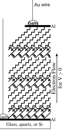
Martin, et. al,19 Metzger et al.20 have studied Langmuir Blodgett (LB) films of γ
-(n-hexadecyl)quinolinium tricyanoquinodimethanide (4) between metal electrodes and observed strong rectification behavior. This molecule is an example of a donor-acceptor
system, but is slightly different than that theorized by Aviram and Ratner. In 4, the donor is the quinolinium moiety (green), connected to the acceptor, tricyanoquinodimethanide
(red) by a π-bridge. The hexadecyl tail facilitates the formation of LB films, as suggested
by the cartoon in Figure 1.10. The head-to-tail arrangement shown in Figure 1.10 was
found to be the most stable structure of the LB film.
N
C16H33
C N
C N
C N
The systems that Aviram and Ratner examined were composed of neutral ground
state donor-acceptor species that became selectively zwitterionic:
+
−
−
−
+
← 9
eV
→D
ó
A
A
ó
D
eV
2
1
A
ó
D
The nature of 4, however, until Metzger’s work, was unclear. It was theorized that the ground state was a mixture of zwitterionic and neutral molecules, and that intramolecular
electron transfer gave rise to the rectification.
Metzger et al. made LB films of 4 on Al pads on quartz, then evaporated a second Al pad on top, with the film at 77K. Connections to the metal pads were made with Ga/In
Glass, quartz, or Si Al Al
Ga/In
Ga/In
Au wire
E
le
ct
ro
n
F
lo
w
fo
r
V
>
0
Figure 1.10 - Cartoon representation of LB film structure of 5 on Al. The one and four monolayer films have the same orientation of the molecule.
A
B
eutectic or Ag paste. Electrical measurements showed strong rectification. Figure 1.11
shows the I-V curves from two different experiments using 4. In Figure 1.11a, a single monolayer of 4 was sandwiched between two Al electrodes. The rectification ratio (RR - identical to the “asymmetric ratio” of Aviram and Ratner) for this sample is ~40. In
Figure 1.11b, four LB monolayers were measured with Al electrodes as well. The RR is
better than 10 in this sample.
Upon consideration of the LB film construction (Figure 1.10), a mechanism for the
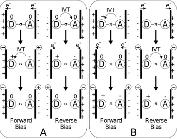
rectifying behavior may be understood. In the previously proposed Aviram-Ratner
model, electron transfer to and from metal electrodes to a neutral ground state molecule
(Figure 1.12, Panel A, forward bias) creates a zwitterionic form that is amenable to
intervalence transfer (IVT) to regenerate the neutral form, with an overall electron
transfer from acceptor towards donor. If the process is initiated in a zwitterionic molecule
(such as 4), under forward bias the IVT occurs first, creating a neutral molecule (Figure 1.12, Panel B, forward bias), followed by electron transfer to and from the metal to
Forward Bias
Reverse Bias
D
0A
0e- e-+ + + +
-D
+A
-e- e-+ + + + -0 0
D
A
IVT + + + +-D
+A
-IVT + + + +
-D
0A
0+ + + +
-D
0A
0+ + + + -Forward Bias
D
+A
-IVT + + + +
-D
0A
0e- e-+ + + +
-D
A
+ -+ + + + -Reverse Bias +-D
A
+ + + + -0 0D
A
+ + + + -- IVT e-e-D
A
+ + + +-A
B
recover the zwitterionic form, again with overall electron transfer from acceptor towards
donor. The difference in the magnitude of the responses shown in (between one and four
monolayers) is not entirely clear, but it has been suggested that the larger response from
multiple monolayers is due to defect conduction.21
1.2.2. Wiring Up – Molecular Wires
Molecules that act as rectifiers were simply the first suggested molecular electronics
components, and were initially studied as a test for the feasibility of such molecular
design. There have been many further attempts to develop molecular based components.
One of the requirements to using any molecular electronic component is the ability to
wire it into a device architecture. To connect molecules to one another, or to a macroscopic world, molecular-scale wires are necessary. In an effort to understand the
important characteristics of such a molecular wire, most research in this area has studied
linear, conjugated oligomers.
Aviram described an important (and obvious) characteristic of molecular wires – that
of conductivity.22 Consider two types of molecules: conductors and proconductors. The
conductor can be derived from the proconductor by either an oxidation or a reduction.
φ
V=0
E
fpolythiophene
polythiophenium
A
B
-1e
-H
S S S
H
n
n H S S S
H
n n
For example, polythiophene is a poorly conductive compound. Upon oxidation, it
becomes polythiophenium, a cation, and a much better conductor by virtue of the unfilled
HOMO. This relationship is made clear in Figure 1.13. The simplified energy level
diagrams indicate a molecule between two metal electrodes. In the proconductor, the
HOMO is fully occupied. When a small bias is applied, no current will pass. In the
conductor, however, the HOMO is only partially filled, and a small bias between the
electrodes causes current to flow.
Conductor and proconductor pairs may find usefulness in molecular electronics,
however, the need to oxidize or reduce them, or introduce a dopant into the bulk makes
them less than ideal. Recent work into metal containing carbon chains and porphyrinic
arrays has provided a possible route around this limitation.
Gladysz and coworkers23 have synthesized metal-terminated carbon chains similar to
5, with n up to 10 (indicated as ReCnRe). Cyclic voltammograms (CV) of three of these
Re PPh3
NO
Re
Ph3P
ON
n
5
Figure 1.14 - A) CVs of three polyynediyl species, 10-5 M in 0.1 M Bu4N
+ BF4
-/CH2Cl2 at 22.5±1 °C, Pt working and counter electrodes, potential vs Ag wire
pseudoreference, scan rate = 100 mV/s, ferrocene = 0.46 V; B) Plot of CV results for series from ReC2Re to ReC10Re, E1 is first oxidation, E2 is second oxidation,
Ep,c and Ep,a are cathodic and anodic peak potentials, respectively. Reproduced with
molecules is shown in Figure 1.14a. For the shorter ReC2Re, two single electron oxidations are observed. For longer chains (ReC3Re and ReC4Re), the oxidation becomes increasingly irreversible. The solution cyclic voltammetry results for the entire
family of complexes from n = 2 through 10 is shown in Figure 1.14b. The presence of only a single, presumably 2e- oxidation peak in ReC10Re indicates that once the chain reaches this length, the metals are effectively isolated from one another and do not
communicate via the conjugated bridge. These molecules have not been studied under
electrode-bound device conditions. However, these results indicate that such a molecule
will not be expected to function as an ideal molecular wire.
Potential molecular wires composed of fused porphyrin rings have also been
constructed. Crossley and Burn24,25 and others have synthesized oligomeric linear
porphyrin arrays (such as 6), and over 100 such systems (e.g., 7) have been studied computationally by Reimers et al.26 in an effort to gauge their potential as molecular wires. Their results suggest that the molecular wire characteristics of these fused ring
porphyrins are highly tunable, depending on the substitution of the porphyrin ring, the
nature of the bridging unit (1,4,5,8-tetra-azaanthracene in 6 and 7), and the metal (or lack thereof) in the system. They observe that the electronic properties of these systems (and
N H N H N N N N N
N NH
N H N N N N N
N NH
N H N N N N N
N NH
N H N N t-Bu t-Bu t-Bu t-Bu t-Bu t-Bu t-Bu t-Bu t-Bu t-Bu t-Bu t-Bu t-Bu t-Bu t-Bu t-Bu t-Bu t-Bu t-Bu t-Bu t-Bu t-Bu t-Bu t-Bu t-Bu t-Bu t-Bu t-Bu t-Bu t-Bu t-Bu t-Bu 6 N H N H N N N N N
N NH
N H N N N N N
N NH
N H N N N N N
N NH
N H N N
7
Et2N3
R R R R R R R R R R R R R R R
R
SiMe3
presumably others) are dominated by the degree of π-delocalization – in π-systems that
localize into single and double bonds, the electrons are locked in place and there is little
communication from one end of the molecule to the other. Highly delocalized systems,
however, support long-distance communication between parts of the molecule, and thus
are desirable in molecular wires. This computational work has laid a significant
groundwork to understanding the experimental behavior of such molecules.
A large body of experimental work has emerged regarding the electronic behavior of
oligo(phenylene ethynylene)s, similar to 8. Tour and co-workers have synthesized many of these molecules, with the longest being 8,27,28 with a length of 128 Å. While this particular molecule has not been experimentally investigated, a number of significant
experiments have been performed on similar shorter molecules to measure their
effectiveness as molecular wires.
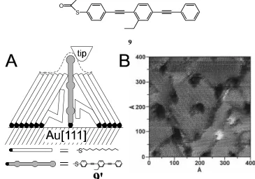
Bumm et al.29,30 used the tip of a scanning tunneling microscope (STM) to measure
the conductivity of single molecular wire molecules (9) embedded in a background
S O
9
composed of dodecanethiolate (DT) SAM. When the thioacetate group on 9 was deprotected to the thiol (9' - Figure 1.15a) in the presence of the crystalline SAM, single molecules, or at most a few molecules, were bound to the underlying Au(111) surface at
disordered defects in the SAM. STM imaging revealed bright, stable, isolated spots at
domain boundaries and defect sites in the DT SAM (Figure 1.15b). These bright spots
were consistent in size, shape and orientation, indicating that they were features sharper
than the tip used to image them.
In addition, Bumm et al. measured the apparent tunneling barrier height (ATBH)
over DT and 9'. The ATBH, a measurement of the conductivity of the underlying film, may be determined by modulating the position of the STM tip (z) and observing the change in the current (I) with respect to the position (dI/dz). There are many convoluting factors, such as mechanical distortion of the film or tip, in determining a quantitative
measure of ATBH. By comparing the ATBH over DT with that over 9', these factors could be ignored and a relative measure of conductivity obtained. The ATBH over 9' was observed to be at least two times higher than over DT. The bright spots in Figure 1.15b
SH HS
10
A
B
indicate the tip withdrawing from the surface, and thus increasing the tip-substrate
separation. Considering that the tip is farther away from the substrate, and the ATBH is
larger, it was inferred that molecules of 9' have a greater conductivity than molecules of DT.
These results suggest that oligo(phenylene ethynylene)-type molecules might make
good molecular wires. However, an experiment performed by Doescher et al.31 suggest
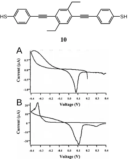
that these molecules are not, in fact, very good molecular wires. Very similar to 9' above,
10 is a dithiol. SAMs of 10 on Au electrodes were found to passivate the Au electrode in a manner similar to DT (Figure 1.16). Anodic stripping voltammetry (ASV) of Cu shows
that deposition of Cu occurs at high negative potentials on both DT and 10. This process happens on bare Au at ~-0.1 V. Cu ions require a significant overpotential to be reduced
at defect sites in a DT SAM,32 and the same effect is observed in SAMs of 10. It would be expected that if 10 were a significant conductor, deposition would be observed at potentials closer to that observed on bare Au.
In a further experiment, Cu was vapor deposited onto each of the SAMs in an
attempt to ensure that a layer of Cu was present atop the defect-free portions of the SAM.
Stripping voltammetry on both DT and 10 SAMs revealed the characteristic stripping peak for Cu at +0.1 V. In Figure 1.17a, DT also showed a broad peak at +1.2 V indicative
of Au oxidation, and the corresponding stripping peak for the oxide at +0.9 V. In Figure
0.8 1
0
-2 -1
-3
0.9 1.0 1.1 1.2 1.3 1.4 1.5 Voltage (V)
Current
(
A)
µ
0.8 2
0
-4 -2
-6
0.9 1.0 1.1 1.2 1.3 1.4 1.5 1.6 Voltage (V)
Current
(
A)
µ
A
A
B
1.17b, a SAM composed of 10 also showed a peak at +1.2 V, but the peak was much sharper than that of DT. A second sweep on the 10 SAM revealed the Au oxidation peak that was hidden beneath this sharper peak. 10 also showed a peak at +1.4 V that was assigned as the oxidation (and subsequent desorption) of the 10 molecule. The nature of the sharper peak at +1.2 V was made clear when the surface was examined by Scanning
Electron Microscopy (SEM). When the Cu-covered 10 SAM was swept to +0.9 V (point A in Figure 1.17b) then removed from the electrochemical cell, SEM images revealed the
presence of Cu islands on top of the 10 SAM. SEM images of the SAM after sweeping past the +1.2 V sharp peak show that the islands were gone. Thus the initial sharp peak at
+1.2 V on the 10 SAM was due to stripping of the Cu islands that are on defect-free, ordered domains of the 10 SAM.
The large overpotential (1.1 V) across the molecule (25.2 Å) indicates an electric
field strength of ~450 MV/m, suggesting a tunneling mechanism and therefore, a tunneling barrier. Charge tunneling through 10 occurs via holes or electrons as charge carriers. Holes must tunnel through a barrier equal to the difference between the Au
Fermi energy and the 10 HOMO. The barrier height for electron tunneling is the difference between the Cu Fermi energy and the 10 LUMO. Whichever barrier height is lower will dictate the dominant charge carrier in the molecule. It is also the case that the
barrier height can be approximated by the overpotential. Thus an overpotential of 1.1 V is
a crude measure of a barrier height of 1.1 V. The formal oxidation of 10 occurs at +1.4 V, very near to the Cu stripping peak at +1.2 V, suggesting that the dominant charge carriers
are holes injected from the Au electrode into the HOMO of 10. Further estimates of the barrier height by independent methods corroborated the 1.1 V measurement. The authors
conclude that a barrier height of 1.1 V is unusual for a molecule intended to be a
conductor. While at odds with predictions that such molecule should be a good
conductor, the authors concede that there are likely differences in the electrical
environment of the molecule when probed by a sharp STM tip versus a planar Cu contact.
In any effort to describe a “molecular wire”, perhaps the most important
characteristic is the “conductivity” of the wire. In other words, how effectively, both
through time and distance, is charge transferred from one end of the molecule to the
rates. In real terms, the rate of electron transfer shows an exponential dependence on
distance. Determining the distance dependence of electron transfer allows comparison of
the “conductivity” of different molecules, regardless of their length. This distance
dependence may be represented by an experimentally determined value, â, determined
from the slope of a plot of ln(k0) vs. distance. Several conjugated oligomer systems have
been studied as potential molecular wire systems, and their â values are presented in
Table 1.1. It is clear that there are many likely candidates for implementation into
practical systems, once the technical difficulties of actually attaching the molecular wires
between molecular components are overcome.
1.2.3. Static Elements – Data Storage
In contrast to the dynamic nature of a molecular wire, with its ability to transfer
charge from one location to another, a memory device represents a static component. In
the current computational architecture, data is stored in a bit-wise manner – the smallest
part of data is either 0 or 1. In a molecular system, there are a number of ways this might
be realized, including charge storage, positional shifting, or material transformation
Nanotubes and their cousins, the buckyballs, have given fruit to notable efforts to
design nanoscale memories. Rueckes et al.38 have proposed a nonvolatile random access
memory (RAM) based on a suspended crossbar array of nanotubes (Figure 1.18). The
memory element arises from the stability of the nanotubes in one of two configurations.
The authors presented calculations that suggest that, depending on the initial separation
of the nanotubes, there are two energy minima corresponding to the nanotubes remaining
either suspended (OFF) or in-contact (ON). The ON state remains so due to van der
Waals interactions between the two nanotubes, and may be initiated in a separated pair by
applying voltage pulses of opposite polarity to the two crossed nanotubes. The ON state 33
, 34, 35, 36, 37
Table 1.1 – Exponential Decay Constants (â) for various molecular repeat units
Molecular Repeat Unit Calc’d â (Å-1) Expt’l â (Å-1) ref. Oligophenylenevinylene,
1 to 4 repeat units 0.06 33
oligophenylethynyl 0.36 34
Oligoporphyrin-TA, 7 0.045 35
polyene 0.078 36
may be switched to the OFF state by applying a larger voltage pulse of identical polarity
to each of the nanotubes. The device elements may be as small as 5 nm, giving a density
of 1012 devices per cm2. The switching time was calculated to be on the order of 10-11 s,
giving an operating frequency of ~100 GHz.
The theoretical work was supported by experimental measurement of a suspended
nanotube junction. The junction was fabricated by mechanical manipulation of nanotubes
and the evaporation of contact electrodes onto them. The device could be switched ON
and OFF with applied voltage pulses. The state of the device could be read by measuring
the resistance of the junction – the resistance in the OFF state was greater by up to 5
orders of magnitude than the ON state. The reading of the device should be
non-destructive, and thus the junction represents a nonvolatile memory element. The authors
proposed to fabricate large arrays of such junctions by either patterned growth of the
nanotubes in an array, or directed self-assembly, both of which have been demonstrated
in different systems.
Kwon and co-workers39 have proposed the use of so-called “bucky-shuttles” as
nonvolatile memory elements. A bucky-shuttle consists of a fullerene (a “buckyball”)
with a diameter close to that of C60 encapsulated inside a short nanotube. These objects
were observed in abundance from the treatment of nanodiamond powder at 1800° C. The
buckyball was observed to stay at one end or the other of the nanotube encapsulation,
presumably due to van der Waals interactions and weak covalent forces, as in crystalline
C60 and nanotube bundles.40 Calculations of the potential energy of a C60 as it shuttles
inside a C240 shell show a 0.24 eV stabilization at the ends of the shell, compared to
anywhere along the length. Reading and writing such a structure necessitates that the
fullerene bear an overall charge. This is accomplished by producing K@C60+, one of a
family of known fullerenes with a caged metal ion. The metal ion within the C60 imparts
a net positive charge that is evenly distributed over the whole fullerene. Writing of data
should occur when a field is applied along the axis of the shell through integrated
electrodes in the ends of the shell. A field strength of ~1.5 V is enough to destabilize one
of the energy minima, causing the K@C60+ to migrate to the other in ~4 ps. The state of
the device can be read nondestructively by measuring the polarity of the capsule, or
destructively by applying a probe voltage and measuring the resulting current pulse.
The authors envision arrays of these capsules packed side by side, with crossing
electrodes connected to their ends as in Figure 1.19. Individual element addressing is
carried out by applying read or write pulses to crossed electrodes, thereby reading from
or writing to the element between them. Under ideal conditions, such an element may be
switched at a rate of 100 GHz. The authors did not suggest any method by which an array
of closely packed, vertically oriented nanotube-based memory elements might be
produced, and thus did not present any predictions on element density.
Other examples of data storage proposals involve the modification of polymeric
materials. While such examples of data storage are not truly molecular electronics, they
bear consideration in the context of discussing the current state of the field. Binnig et al.41