Design of a High Frequency Dual Modulus
Prescaler using Efficient TSPC Flip Flop using
180nm Technology
Divya shree .M
1, H. Venkatesh kumar
2PG Student, Dept. of ECE, Nagarjuna College of Engineering & Technology, Devanahalli, Karnataka, India1
Associate Professor, Dept. of ECE, Nagarjuna College of Engineering & Technology, Devanahalli, Karnataka, India2
ABSTRACT: A high speed efficient TSPC flip-flop divide-by-16/17 dual modulus prescaler is proposed. The efficient (proposed) TSPC flip-flop with split path not only reduces the clock load and decrease power but also increases the speed of operation. The speed of the precaler can improve in two aspects. First is by adopting a new pseudo divide-by-2/3 prescaler, the minimum working period is reduced by half a NOR gate’s delay. Second is by changing the connection of TSPC D-Flip-flops, the minimum working period is reduced by half an inverter’s delay. The proposed circuit is capable of operating up to 1.8GHz and is implemented in 5V, 0.18um CMOS technology. Simulations and designs are performed on Cadence Virtuoso and Spectre tools using UMC 0.18um technology.
KEYWORDS: Dual-Modulus Prescaler, efficient TSPC, divide-by-2/3, divide-by-16/17 prescaler.
I.INTRODUCTION
Dual-modulus frequency prescaler plays an main role in phase-locked loop (PLL) designs[1]. In spite of fact that current-mode logic and inject locking prescaler can provide working frequency of hundreds/tens GHz with process of SoI CMOS or InP DHBTs and so on. TSPC dual-modulus prescaler is greatly utilized in several GHz with standard CMOS process[2],[3]. TSPC prescaler has the merits of single clock phase, low power, small area, and large output swing. Speed improvement is an important design issue for TSPC prescaler. In addition to the above, several techniques have been developed. At the transistor level decreasing the threshold voltage of nMOS transistors, forward body biasing technique can improve the speed, but it suffers from increased cost and decreased robustness as well as high minimum working frequency[4]. At the gate level, by adopting E-TSPC(extended-true single phase clock) flip- flops can effectively improve the operating speed performance. But the serious is current leakage, thus the performance of the minimum working frequency is limited. At the RTL level, speed improvement of divide-by-2/3 prescaler can also increases in improving the speed of divide-by-16/17 prescaler. However, several TSPC circuit design rules are broken in these paper. It mainly leads to shrinking the range of frequency because these prescalers are not suitable for low frequency operation for longer time.
II. RELATED WORK
A low-power true single-phase-clock (TSPC) based domino logic circuit design. Compared to using three clock transistors in the conventional TSPC-based scheme, the proposed circuit only requires two transistors. As a result, the clock load capacitance is reduced, leading to low power consumption in the clock distribution network. A keeper design to solve charge sharing is also demonstrated. Simulation results using 90nm and 45nm CMOS technologies are provided and discussed, respectively, which illustrate power saving as compared to conventional design not only when the input logic is active but also when the input logic is held to zero.
Two dynamic circuit techniques, raising only a single-phase clock which is never inverted[6]. This class of circuits has the advantages of simple clock distribution, small area for clock lines, reduced clock skew problems, and high speed. Several examples are demonstrated.
Implementation of a dual modulus prescaler using an extension of the true-single phase-clock (TSPC) technique, the extended TSPC (ETSPC), is presented. The E-TSPC consists of a set of composition rules for single-phase-clock circuits employing static, dynamic, latch, data precharged, and NMOS-like CMOS blocks. The composition rules, as well as the CMOS blocks, are described and discussed.
II. TPC D-FLIPFLOP
Fig 1.structure of TSPC DFF.
Fig1.shows a popular structure of TSPC D-flipflop. The circuit consists of blocks called n-blocks and p-blocks of four alternating stages. Single clock signal drives the each block. In this design single global clock signal is generated and distributed in order to simplify the design[7]. fig.1 shows the schematic of TSPC D-flip flop consists of 11 transistors, this positive edge triggered flip flop uses just a single clock signal for synchronization. During the ON period of clock whatever is the value of input it will become’s an output.
Now another design of TSPC D-flipflop with 10 transistors is shown in fig2,which consumes less number of transistor’s and area compared with previous one and it also reduces power consumption. The proposed TSPC with split path not only reduces the clock load and decreases power but also increases the speed of operation.
The true single-phase clock(TSPC)is common dynamic flipflop which performs the flipflop operation with little power and at high speeds. The setup time of the TSPC DFF can be written as
tsetup = tD− A ……….(1)
Where tD− A means the propagation time from node D to node A, which is a clocked inverter’s delay. The propagation delay of the TSPC DFF can be written as
td−Q N = tA− B + tB−QN
td− Q = tA− B + tB−QN + tQN− Q ………(2)
where td−QN and td− Q are the propagation delay from CLK to QN and Q.respectively. tA− B, tB−QN, tQN− Q represents the propagation delay from node A to B, B to QN, and QN to Q, respectively.
III. CONVENTIONAL DIVIDE-BY-16/17 DAUL MODULUS PRESCALER
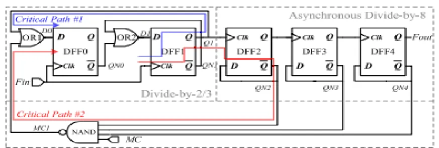
Fig 3: structure of Conventional divide-by-16/17 prescaler
Fig.3 shows the schematic of a conventional divide by 16/17 prescaler. These prescaler is designed based on a divide-by-2/3 prescaler. It consists of a divide-divide-by-2/3 prescaler, an asynchronous divide by 8 divider, four input NAND gate and a two OR gates. It has two critical paths.
First, critical path#1(Q1 path) comes through D-FF1and OR1.
Fig 4: schematic of Conventional divide-by-16/17 prescaler
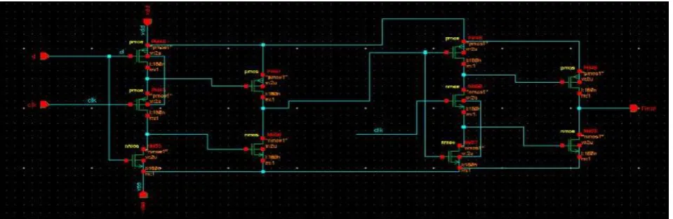
Fig.4 shows the schematic of Conventional divide-by-16/17 prescaler is implemented by using fig3 as reference in 180nm technology.
Within a period of Fin, signal must pass path#1 while within a periods of Fin it should pass path#2.theoritically, it is critical to identify which path decides the minimum working period. But the result varies in different designs. In conventional divide by 16/17 prescaler there is a trade-off between lengths of the two critical paths. The optimized design is to make the length of critical path #1 approximately equal to half length of critical path #2.
In conventional divide-by-16/17 prescaler, In front of DFF0 two logic gates (NAND and OR1) are located. In addition, there are two critical paths. Apparently, It is not the optimized design .To achieve a high speed both the critical paths should be optimized, which is a great challenge for designers.
IV. PROPOSED DIVIDE-BY-16/17 DAUL MODULUS PRESCALER
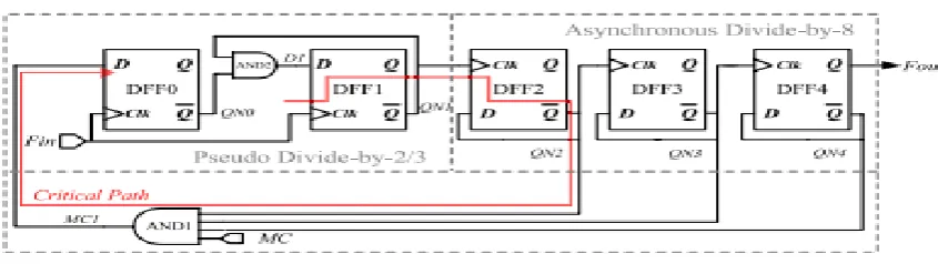
Fig 5: structure of proposed divide-by-16/17 prescaler
Fig 6: schematic of proposed divide-by-16/17 prescaler
The operation mode of proposed circuit is as follows. When MC = 1, MC1 changes its value according to (QN2, QN3, QN4).The pseudo divide-by-2/3 prescaler controlled by MC1 accomplishes seven times of divide-by-2 operations and one time of divide-by-3operation in a cycle. The whole circuit operates in divide-by-17mode. When MC = 0, MC1 keeps low and the pseudo 2/3prescaler keeps on 2 operation. The whole circuit works in divide-by-16 mode.Fig 6 shows the schematic of proposed divide-by-divide-by-16/17 prescaler implemented by using fig 5 as reference in 180nm technology.
V. MEASUREMENT RESULTS
TABLE 1: power and delay comparison
The above table1 shows the power and delay comparison of normal TSPC flip-flop (positive edge)and proposed TSPC flip-flop. The power and delay consumption of proposed TSPC flip-flop is less compared to normal TSPC flip-flop and the proposed TSPC flip-flop circuit consists of less number of transistors then the normal TSPC flip-flop.
TABLE 2: frequency calculations
The above table2 shows the frequency calculation for two different frequencies, when control signal is high the circuit performs divide-by-2 operation, means it will divide the clock frequency by 2,when control signal is high. when control signal is low, the circuit performs divide-by-3 operation, means it will divide the clock frequency by 3,when control signal is low.
TSPC flip-flop power delay
pos_edge TSPC flip-flop 10.46e-6 20.1e-9
Modified pos_edge TSPC flip-flop
3.217e-6 20.04e-9
frequency Divide by 2 operation Divide by 3operation
1Ghz 1G/2 500M 1G/3 333.33M
TABLE 3: frequency calculations
The above table3 shows the frequency calculation for two different frequencies, when control signal is high the circuit (fig. 5) performs divide-by-17 operation, means it will divide the clock frequency by 17,when control signal is high. When control signal is low, the circuit performs divide-by-16 operation, means it will divide the clock frequency by 16,when control signal is low.
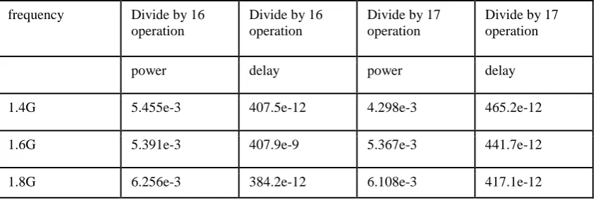
TABLE 4: power and delay comparison of conventional divided by 16/17 prescaler
TABLE 5: power and delay comparison of proposed divided by 16/17 prescaler
The above table 4 & 5 shows the power and delay comparison of conventional and proposed divide-by-16/17 prescaler. The proposed divide-by-16/17 prescaler consumes less power and delay compared to the conventional divide-by-16/17 prescaler for different frequencies as shown in the above table.
frequency Divide by 16 operation Divide by 17 operation
1Ghz 1G/16 62.5M 1G/17 58.82M
1.8Ghz 1.8G/16 112.5M 1.8G/17 105.88M
frequency Divide by 16
operation
Divide by 16 operation
Divide by 17 operation
Divide by 17 operation
power delay power delay
1.4G 5.669e-3 1.22e-9 5.334e-3 1.22e-9
1.6G 5.66e-3 1.086e-9 5.84e-3 1.086e-9
1.8G 6.315e-3 980.7e-12 6.607e-3 980.6e-12
frequency Divide by 16
operation
Divide by 16 operation
Divide by 17 operation
Divide by 17 operation
power delay power delay
1.4G 5.455e-3 407.5e-12 4.298e-3 465.2e-12
1.6G 5.391e-3 407.9e-9 5.367e-3 441.7e-12
VII.SIMULATION RESULTS
Fig.7 waveform of proposed divide-by-16 operation
The fig 7 shows measured output waveform of the proposed divide-by-16 prescaler at 1.8GHz input frequency in divided by 16 mode. The first waveform is clock signal which is taken as an input. The second waveform is the control signal and the third waveform is the output waveform.
Fig8: waveform of proposed divide-by-17 operation
The fig 8 shows measured output waveform of the proposed divide-by-17 prescaler at 1.8GHz input frequency in divided by 17 mode. The first waveform is clock signal which is taken as an input. The second waveform is the control signal and the third waveform is the output waveform.
VII. CONCLUSION
This brief presents a novel high speed TSPC divide-by-16/17 dual modulus prescaler. The proposed TSPC with split path not only reduces the clock load and decreases power but also increases the speed of operation which in turn reduces total power consumption in divide-by-16/17 prescaler. The speed of precaler is improved in two aspects. First is by adopting a new pseudo divide-by-2/3 prescaler, the minimum working period is reduced by half an NOR gate’s delay. Second is by changing the connection of TSPC D-Flip-flops, the minimum working period is reduced by half an inverter’s delay. Fabricated in 0.18um CMOS technology, the proposed circuit achieves a 1.8GHz maximum working frequency.
REFERENCES
[1] T. Shibasaki, H. Tamura, K. Kanda, H. Yammaguchi, J. Ogawa, and T. Kuroda, “A 20-GHz injection-locked LC divider with a 25% locking
range,” in Int. Symp. VLSI Circuits Dig. Tech. Papers, Jun. 2006, pp. 170–171.
[2] D. D. Kim, J. Kim, and C. Cho, “A 94GHz locking hysteresis-assitedand tunable CML static divider in 65nm SOI CMOS,” in IEEE ISSCC
Dig. Tech. Papers, Feb. 2008, pp. 460–628.
[3] D. A. Hitko, T. Hussain, D. S. Matthews, R. D. Rajavel, I. Milosavljevic, and M. Sokolich, “State of the art low power (42 mW per flip- flop)
[4] B. Chang, J. Park, and W. Kim, “A 1.2 GHz CMOS dual-modulusprescaler using new dynamic D-type flip-flops,” IEEE J. Solid-State Circuits, vol. 31, no. 5, pp. 749–752, May 1996.
[5] C.-Y. Yang, G.-K. Dehng, J.-M. Hsu, and S.-I. Liu, “New dynamic flip-flops for high-speed dual-modulus prescaler,” IEEE J. Solid-State
Circuits, vol. 33, no. 10, pp. 1568–1571, Oct. 1998.
[6] S. Kim and H. Shin, “An E-TSPC divide-by-2 circuit with forward body biasing in 0.25 μm CMOS,” IEEE Microw. Wireless Compon.
Lett.,vol. 19, no. 10, pp. 656–658, Oct. 2009
[7] H. Shin, “A 1-V TSPC dual modulus prescaler with speed scalability using forward body biasing in 0.18 μm CMOS,” IEICE Trans. Electron.,