Vol. 3, Issue 3, March 2015
Multi Threshold Low Power SRAM
Using Floating Gates
Sushree Sangita Das
1, Kanan Bala Ray
2, Prangya Parimita Nanda
3PG Student, School of Electronics Engineering , KIIT University, Bhubaneswar, Odisha, India1 Asst. Professor, School of Electronics Engineering, KIIT University, Bhubaneswar, Odisha, India2
PG Student, School of Electronics Engineering, KIIT University, Bhubaneswar, Odisha, India3
ABSTRACT: We investigate the mechanism of threshold voltage shifting of SRAM based on floating gates. Multi threshold SRAM based on floating gates is represented in this paper to reduce the power consumption and leakage current. By using multi threshold technique in SRAM based on floating gates, it consumes 66.39% less power for write'1' operation, 56.21% less power for write'0' operation, 23.35% less power for read'1' operation and 34.66% less power for read'0' operation as compared to SRAM using floating gates. It also consumes 90% less leakage current in hold state as compared to SRAM using floating gates in 180nM technology. For minimizing power consumption and leakage current, the concept of multi threshold is included in this paper.
KEYWORDS: Floating gate, Multi Vth, Transistor Stacking, SRAM.
I. INTRODUCTION
Rapid growth in VLSI fabrication process results in the increase of the densities of integrated circuit by scaling down the technology. But the devices with such high densities lead to high power consumption and run time failure. Supply voltage has been scaled down to maintain low power consumption. Hence to control drive current and to achieve high performance, transistor threshold voltage (vth) scaling leads in the exponential increase of the sub
threshold leakage current [1]. Static random access memory is used in most of the embedded and portable devices because of the high speed [2]. Due to the strong demand of the SRAM memory, reduction of power consumption and leakage current of SRAM memory is very important to improve system performance, efficiency and reliability [2].
The conventional SRAM is composed of two inverters connected back to back and two access transistors to connect bit lines with storage cells. Stability is also an important parameter of SRAM cell design. Stability defines how the memory cell is affected by process verification and operating conditions [3]. Stability can be measured by calculating static noise margin (SNM) , which is the maximum tolerable DC noise voltage at a storage node[3].
This thesis work focuses on reduction of static power using combine of stack and multi threshold voltage principle. Figure 1 shows the structure of stack approach. When more than one transistor in the stack is turned off, the sub-threshold leakage current of a stack of series connected transistors suppresses. This effect is called as stacking effect [1],[4]. In figure 1 when both N1 and N2 transistors are turned off , due to small amount of drain current, the voltage at
intermediate node N (VN) is positive. This positive voltage at intermediate node has three effects.
Due to positive voltage at node N, the gate to source voltage (VGS1) of N1 reduces. Hence the sub-threshold
current decreases [1],[4].
Due to positive voltage at node M, the body to source voltage (VBS1) of N1 becomes negative , resulting in
an increase in the threshold voltage( larger body effect) of transistor N1 and hence reducing the
sub-threshold leakage current[1],[4].
Due to VN>0, the drain to source voltage (VDS) of transistor N1 decreases. So the threshold voltage
Figure 1. Stacking Approach
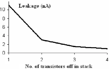
The stacking effect states that the circuit is far less leaky in more than one OFF transistors in the path from supply voltage to ground as compared to a circuit with one OFF transistor in the path [5],[6]. The number of OFF transistors is related to leakage power as shown in figure 2.
Multi threshold voltage CMOS technology provides both high VTH and low VTH transistors in a single chip to
control leakage current problem [7]. The high threshold voltage transistors can reduce leakage current, while low threshold voltage transistors are used for high performance. The structure of multi VTH principle is shown in figure
3.
Figure 2. Transistors Stacking Vs Leakage Current
Vol. 3, Issue 3, March 2015
II. FLOATING GATE MOSFET
The floating gate MOSFET (FGMOS) is similar to a conventional MOSFET. The gate of the FGMOS is electrically isolated and create a floating node in DC [9],[10]. Multiple inputs are deposited through resistors and capacitors above the floating gate and electrically isolated from it. Floating gate MOSFET is completely surrounded by highly resistive material. So the charge stored in it remains unchanged for long period of time. Number of inputs act as floating inputs of the transistor [8],[9].
Figure 4. N channel N input FGMOS Transistor
III. SRAM USING FLOATING GATES
The SRAM using floating gate in 45nm technology is shown in figure 5. The storage node can be directly connected with bit lines through the pass transistors. Voltage deviation mainly occurs due to leakage current and damage the storage nodes [10].
Figure 5. SRAM using Floating Gates
Sizing of the cross coupled inverters and access transistors play an important role to maintain data stability and high speed. For maintaining read stability, the cross coupled transistors M1 andM3 must be stronger than access transistors
M5 and M6. For write stability, the cross coupled transistors M2 and M4 must be weaker than access transistors M5 and
M6. Two input NFGMOS and PFGMOS are implemented in conventional SRAM. One of the inputs of both FGMOSs
and write operation, the access transistors M5 and M6 are in saturation mode. For write '1' operation, BL must be 1 and
BLB must be 0. When WL goes high, the access transistors M5 and M6 turns on and for those transistors M2 and M3 are
on and VDD value is appeared at node A. For read operation, the value which is stored at node A passes towards BL and
node B passes towards BLB and sense amplifier sense the value. For write'0' and read '0' operation, the opposite phenomenon will occur.
IV. MULTI VTH SRAM USING FLOATING GATES
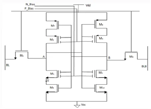
Figure 6 represents multi VTH SRAM using floating gates. The transistors M1 to M6 comprise the SRAM using
floating gates. In both pull up and pull down network, stacking is applied. Transistors M9 and M10 are connected as
NMOS stacking transistors between pull down network and ground. Transistors M7 and M8 are connected as PMOS
stacking transistors between supply voltage and pull up network.
Figure 6. Multi VTH SRAM using Floating Gates
During cell hold state, the node at '0' value is connected to ground through to series connected NMOS off transistors. So, leakage current reduces due to stack effect. Similarly the leakage current flowing through PMOS off transistors in pull up path also reduces due to stacking effect. The power can be reduced by using high threshold voltage transistors. In this memory cell, both high VTH and low VTH transistors are used. M7, M8, M9, M10 transistors are
high VTH transistors. Other transistors are low VTH transistors. Transistors sizing of multi VTH SRAM using floating
gates is same as SRAM using floating gates .
V. SIMULATION RESULTS
In this section comparison between SRAM using floating gates and multi VTH SRAM using floating gates cell has
been carried out on the basis of total power consumption, leakage current delay and SNM in 45nM technology.
A. Total Power Calculation
Vol. 3, Issue 3, March 2015
Table 1: Percentage power improvement in the Multi VTH SRAM using floating gates compared to SRAM using
floating gates.
Operation SRAM using floating gates(µW)
Multi VTH
SRAM using floating
gates(µW)
Improvement
(%)
Write 1 147.1 49.44 66.39 Write 0 215.5 94.36 56.21 Read 1 415.3 318.3 23.35 Read 0 349.4 228.3 34.66
Table 1 shows total power consumption of SRAM using floating gates and multi VTH SRAM using floating gates
and improvements in the proposed design.
B. Leakage Current
Leakage current is calculated in hold state.
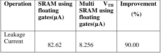
Table 2: Percentage leakage current improvement in the Multi VTH SRAM using floating gates compared to SRAM
using floating gates.
Operation SRAM using floating gates(µA)
Multi VTH
SRAM using floating gates(µA) Improvement (%) Leakage Current
82.62 8.256 90.00
Table 2 shows leakage current of SRAM using floating gate, multi VTH SRAM using floating gates and
improvements.
C. Delay Calculation
SRAM delay is defined as the time taken to change the node voltage from one logic to other logic
.
Table 3: Delays of SRAM using floating gates and Multi VTH using floating gates.
Operation
SRAM using floating gates(ps)
Multi VTH SRAM
using floating gates(ps)
Write 1 12.1 8.27 Write 0 6.59 7.53 Read 1 12.03 8.225 Read 0 6.53 7.52
Table 3 shows delays of different operations for SRAM using floating gates as well as multi VTH SRAM using floating
Stability of the memory cell is measured in terms of static noise margin (SNM) and it is obtained by drawing and inverting the inverter characteristics [11],[12]. It is the length of the size of the maximum square that can fit into the eye of the butterfly curve.
Table 4: Percentage SNM improvement in the Multi VTH SRAM using floating gates compared to SRAM using floating
gates.
Operation
SRAM using floating gates(volt)
Multi VTH
SRAM using floating gates(volt)
Improvement
(%)
Write 1 0.52 0.62 19.23 Write 0 0.1 0.12 20 Read 1 0.5 0.64 28 Read 0 0.1 0.12 20 Hold 0.48 0.66 37.5
Table 4 shows write and read stability of SRAM using floating gates and multi VTH SRAM using floating gates and
improvements in the proposed design.
VI. CONCLUSION
With the aim of low power and high SNM SRAM cell, this multi VTH SRAM using floating gate is designed.
The multi VTH SRAM using floating gates consumes 66.39% less power for write'1' operation, 56.21% less power for
write'0' operation, 23.35% less power for read'1' operation and 34.66% less power for read'0' operation as compared to SRAM using floating gates. It also consumes 90% less leakage current in hold state as compared to SRAM using floating gates. The above circuit is designed and simulated in cadence virtuoso environment in 180nM technology.
REFERENCES
1. Kaushik Roy, Saibal Mukhopadhyay, Hamid Mahmoodi-Meimand, "Leakage Current Mechanisms and Leakage Reduction Techniques in
Deep-Submicro meter CMOS Circuits",Proceedings Of The IEEE, Vol. 91, No. 2, February 2003.
2. Basavaraj Madiwalar, Dr. Kariyappa B.S," Single Bit-line 7T SRAM cell for Low Power and High SNM",978-1-4673-5090-7/13/$31.00
©2013 IEEE.
3. S. K. Singh, S. V. Singh, B. K. Kausik C. Chauhan, T. Tripathi," Characterization & Improvement of SNM in Deep Submicron SRAM
Design",978-1-4799-2866-8/14/$31.00 ©2014 IEEE.
4. Kaushik Roy, Hamid Mahmoodi-Meimand, and Saibal Mukhopadhyay," Leakage Control for Deep-Submicron Circuits",IEEE.
5. B. Dilip,P. Surya Pras Ad & R. S. G. Bhavani," Leakage Power Reduction In Cmos Circuits Using Leakage Control Transistor Technique In
Nanoscale Technology",Ijess , Vol-2 Iss-1, 2012.
6. Preeti Verma, R. A. Mishra," Leakage Power and Delay Analysis of LECTOR Based CMOS Circuits",978-1-4577-1386-611$26.00©2011
IEEE.
7. S.Lakshmi Narayan, Reeba Korah and N.Krishna Kumar," A Novel Sleepy Stack 6-T SRAM Cell Design for Reducing Leakage Power in
Submicron Technologies", International conference on Communication and Signal Processing, IEEE, April 3-5, 2013,India.
8. Andreas Luck, Stefan Jung, Ralf Brederlow, Roland Thewes, Karl Goserand Werner Weber," On The Design Robustness Of Threshold Logic
Gates Using Multi-Input Floating Gate Mos Transistors", IEEE Transactions On Electron Devices, Vol. 47, No. 6, June 2000.
9. Luca Larcher, Paolo Pavan, Stefano Pietri, Lara Albani, And Andrea Marmiroli," A New Compact Dc Model Of Floating Gate Memory Cells
Without Capacitive Coupling Coefficients",Ieee Transactions On Electron Devices, Vol. 49, No. 2, February 2002.
10. Hiroyasu Kondou, Sumio Fukai, Yohei Ishikawa," Multiple-Valued SRAM With FG-Mosfets",1-4244-0387-1/06/$20.00 @2006 IEEE.
11. Saurabh, S. Shekhar, A. Purwar and S. Biswas," New Improved Low Power and High SNM Single Metal SRAM in 32 nm Technology",2014
International Conference on Computer Communication and Informatics (ICCCI -2014), Jan. 03 – 05, 2014, Coimbatore, INDIA,
978-1-4799-2352-6/14/$31.00 ©2014 IEEE.
12. Evert Seevinck, Frans J. List, And Jan Lohstroh," Static-Noise Margin Analysis Of Mos Sram Cells",Ieee Journal Of Solid-State Circuits, Vol.
Vol. 3, Issue 3, March 2015
BIOGRAPHY
Sushree Sangita Dasis a PG student of VLSI Design & Embedded System in the Electronics Department, School of Electronics Engineering, KIIT University. She received Bachelor of Technology (BTech) degree in 2012 from BCET, Balasore, Odisha, India. Her research interests are low power VLSI design, memory design etc.
Kanan Bala Ray is an Asst. Prof. in the Electronics Department, School of Electronics Engineering, KIIT University. She is perusing Ph.D from KIIT University. She received Master of Technology (MTech) degree from KIIT University, Odisha, India. Her research interests are low power VLSI design, memory design etc.