Implementation Design of LDPC Decoder
Using FPGA
Ilakkiya S N 1, Nevetha R 2, Sarathy S 3, Swetha S 4, Deepa R 5
P.G. Student, Embedded System, Bannari Amman Institute of Technology, Sathyamangalam, Tamilnadu, India1 2 3 4
Associate Professor, Department of Electronics and Instrumentation Engineering, Bannari Amman Institute of
Technology, Sathyamangalam India5
ABSTRACT: In this work, we present a FPGA design and implementation of a parallel architecture of a low complexity LDPC decoder for high data rate applications. The selected code is a regular LDPC code (3, 4). VHDL design and synthesis of such architecture uses the decoding by the algorithm of BP (Believe propagation) simplified "Min-Sum". The complexity of the proposed architecture was studied; it is 6335 LEs at a data rate of 2.12 Gbps for quantization of 8 bits at the second iteration.Low Density Parity Check (LDPC) codes have become very popular now-a-days because of their Shannon limit approaching error correcting capability and hence have been used in many applications. This paper demonstrates a flexible Low Density Parity Check (LDPC) decoder which is an improvement over other existing work on a general LDPC decoder.
KEYWORDS: Error correcting codes; LDPC codes; BP
“
Min-Sum”; VHDL language; FPGA.I. INTRODUCTION
LDPC codes were discovered by Gallager [1] [2] in the early 1960. This remarkable discovery has been largely ignored by researchers for nearly 20 years, until the work of Tanner in 1981, in which he provided a new interpretation of the LDPC codes from a graphical perspective. Tanner's work has also been ignored by theorists for about 14 years until the late 1990s, when some coding researchers began to investigate the graphic codes and iterative decoding. Their research led to the rediscovery of Gallager’s codes. Error correction coding is a means which deals with detection and correction of errors which are introduced into a communication system by the receiver.Shannonpublished a paper in 1948 that revolutionized communications. He found that there is a fundamental limit to how muchin formation can be reliably sent over a channel (its capacity) with respect to the noise present in the system.Low Density Parity Check (LDPC) Codes are a class of block code that satisfies both randomness and increased length.
ISSN(Online): 2319-8753 ISSN (Print): 2347-6710
I
nternational
J
ournal of
I
nnovative
R
esearch in
S
cience,
E
ngineering and
T
echnology
(A High Impact Factor, Monthly, Peer Reviewed Journal) Visit: www.ijirset.com
Vol. 8, Issue 4, April 2019
into the memory unfortunately; this approach is too slow for any operation except simulations [3]. The number of clock cycles required for each iteration of the serial decoder is approximately twice the number of edges present.
DECODING OF LDPC CODES:
Decoding the LDPC codes is done from iterative algorithm; the most used is the BP (Belief Propagation). In our work, we have used the BP "Min-Sum" adapted to the hardware implementation. The algorithm consist to update, first the data nodes after, check nodes at each iteration and at the end make a decoding “Hard” decision that is the most likely codeword.
PARTIALLY PARALLEL DECODER:
In a partially parallel decoder design, some check and bit nodes are realized in hardware which involves sharing as in the serial decoder case. There is a trade-off between speed and complexity which results in increase in the number of check and bit nodes when realized in hardware which in turn increases the speed of each decoder iteration [4]. This in turn increases the complexity of the design. Serial and parallel architectures could be considered subclasses of the partially parallel decoder (serial imple mentation has only one bit and check node realized in hardware while parallel Implementation would have all b it and check nodes realized in hardware). The major Disadvantage in this case is me mory collision. If two nodes try to access the same me mory during the same clock cycle a collision occurs and one of the nodes has to stall for a cycle which in turn decreases the throughput of the decoder.
ENCODING OF LDPC CODES:
The encoding operation consists first in finding a generator matrix G such that G.HT = 0. The work of T. J. Richardson and Urbanke R.L that the check matrix must undergo a preprocessing before the encoding operation. The aim of this pre-processing is to put this matrix in a lower pseudo-triangular form, using only permutations of rows or columns. This matrix is composed of 6 sparse sub-matrix, referenced A, B, C, D, E and a lower triangular T sub-matrix. The size of T sub-matrix is (m-g)×(m-g) where g is smaller as possible. Once the H pre-processing is completed, the coding principle is based on the resolution of the system represented by the equation C.HT=0T.
III.FULLYFLEXIBLEDECODERARCHITECTURE
The design is based on scheduling as described in [15] by Maseraet al. The proposed design imple mentation is based on both partially parallel imp le mentation and uncast messages while the design proposed by Maseraet al is based on multicast messages.
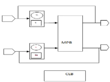
Fig 1 : Top Block Diagram For Decoder
INITIALIZATION:
During initialization, channel measure ments are loaded into the bit processor block.
BIT TO CHECK:
During the bit to check half iteration, the bit node processor performs the bit node function as described in the equation below
In the first half iteration there are no incoming messages and the processor outputs the channel measurement. The messages flow from the bit node processors through the message permuting block and then to the corresponding check node processor in order.
CHECK TO BIT:
During the bit to check half iteration, the check node processor performs the check node function as described
in the equation below,
The messages flow from the check node processors
through the message permuting block and then to the
ISSN(Online): 2319-8753 ISSN (Print): 2347-6710
I
nternational
J
ournal of
I
nnovative
R
esearch in
S
cience,
E
ngineering and
T
echnology
(A High Impact Factor, Monthly, Peer Reviewed Journal) Visit: www.ijirset.com
Vol. 8, Issue 4, April 2019
IV.EXPERIMENTAL RESULTS
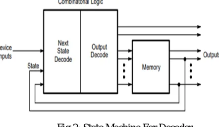
After a number of iterations of bit to check and check to bit cycles the decoder moves to the output stage
Fig 2: State Machine For Decoder.
The MPB decides the flexibility of the decoder. Its purpose is to connect the bit node processor to the check node processor (and vice versa), so that the check node processor receives the incoming messages in a order as depicted in the Tanner graph. The control unit is responsible for implementing the state machine. The configuration for the code is stored in a ROM b lock within the control unit which contains information about the time varying settings for the Benes network and the inter leaver banks in the message permutation unit. It also assigns the appropriate bit and check nodes to the respective processors.
DESIGN APPROACH:
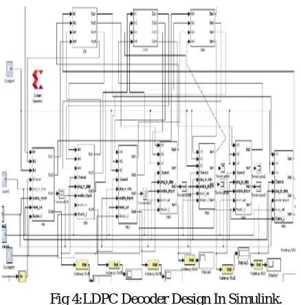
System generator is very flexible in integrating different design approaches namely Simu link models and VHDL codes. Simulink provide a much higher level of abstraction than VHDL. Therefore, our design approach utilizes Simulink library blocks to design various modules of the proposed decoder architecture and the VHDL code for the same is generated automatically using system generator [5]. The auto-generated VHDL code can also be used in Xilinx ISE (Integrated Software Environment) for synthesis and imp le mentation on desired FPGA (Field Programmable Gate Array). Automatic VHDL code generation reduces design efforts hence increases design productivity.
DECODER DESIGN:
Our decoder design architecture mainly consists of two Processors i.e. Check Node Unit Processor and Variable Node Unit Processor. A generic Simulink model was first developed for the variable node and check node.
VARIABLE NODE DESIGN USING SIMULINK:
Fig 3: Variable Node Design In Simulink
It uses blocks from Simulink library (absolute and bitwise XOR Xilinx blocks). The check node finds the minimum of
all the inputs and performs the parity checks. Finally, the fully flexible LDPC decoder design using Variable node and
ISSN(Online): 2319-8753 ISSN (Print): 2347-6710
I
nternational
J
ournal of
I
nnovative
R
esearch in
S
cience,
E
ngineering and
T
echnology
(A High Impact Factor, Monthly, Peer Reviewed Journal) Visit: www.ijirset.com
Vol. 8, Issue 4, April 2019
FPGA IMPLEMENTATIONAND SIMULATION RESULTS:
We implement this LDPC decoder in Xilinx Hardware Description Language andSynthe size it using ISE (Ver.
13.4). The code is downloaded onto the xc6slx16 device of Spartan 6 family using csg324 package. The board was
NEXYS 3 from DIGILENT spartan6. The table below summarizes the design statistic results of FPGA for the desired
LDPC decoder.
V. CONCLUSION
This paper has undergone an extensive review of the existing research works on Flexible LDPC decoder and flexible LDPC decoders. We have designed a fully flexible LDPC decoder by using partially parallel imple mentation and the decoder is found to run at a clock speed of 11.2ns (Maximum frequency of operation being 89.29M Hz). Based on these results, we conclude that the proposed architecture provides better solution for high speed decoding and also takes lesser area. Hence TAR increases which is better than the previous architectures.
REFERENCES
[1] C. Shannon, “A mathematical theory of communication," Bell System Technical Journal, vol. 27, no. 1, pp. 379-423, 1948.
[2]S.-Y. Chung, J. Forney, G.D., T. Richardson, and R. Urbanke, “On the design of low density parity check codes within 0.0045 db of the Shannon limit," Communications Letters, IEEE, vol. 5, no.2, pp. 58-60, Feb 2001.
[3]R. Gallager, “Low-density parity-check codes," Information Theory, IEEE T transactions on, vol. 8, no. 1, pp. 21-28, Jan 1962.
[4]D. J. C. MacKay, “Good error-correcting codes based on very sparse matrices,” IEEE Trans. Inf. Theory, vol. 45, no. 2, pp. 399–431, Mar. 1999. [5]G. Madera, F. Quaglio, and F. Vacca, “Implementation of a flexible LDPC decoder, “Circuits and Systems II: Express Briefs, IEEE Transactions on, vol. 54, no. 6, pp. 542-546, June 2007.
[6]V. G. Chris Winsted, Nhan Nguyen and C. Schlegel, “Low-voltage comes circuits for analog iterative decoders," Circuits and Systems, IEEE Transactions on, vol. 53, Apr. 2006.