Copyright to IJAREEIE www.ijareeie.com 1922
Design of Current-Mode Sinusoidal
Oscillators Using Single FTFN
Mukesh Kumr
1, Dharam Vir
2,Dr. Pradeep Dimri
3Research Scholar, Department of Electronics Engg, YMCA University of Science & Technology, Faridabad, Haryana, India 1
HOS, Department of Electronics Engg, YMCA University of Science & Technology, Faridabad, Haryana, India 2 A.P, Department of Electronics Engg, YMCA University of Science & Technology, Faridabad, Haryana, India 3
Abstract:This paper presents a current-mode quadrature oscillator. We propose an oscillator that can provide two sinusoidal output currents with 90deg phase difference. It also provides high output impedance that enables the circuit to directly drive load without additional current buffer. The condition of oscillation and frequency of oscillation can be controlled independently and electronically by adjusting the bias currents of the CCTAs. The circuit uses three current controlled transconductance amplifiers (CCTAs) and two grounded capacitors. The proposed circuit uses only grounded capacitors without additional external resistors, the proposed circuit is considerably appropriate to further developing into an integrated circuit. The results of PSPICE simulation program are corresponding to the theoretical analysis. The proposed circuits use single four-terminal floating nullor and, at most, eight passive elements. Two of the oscillator circuits are grounded capacitors and enjoy the independent grounded-element control of the frequency of oscillation and the condition of oscillation. Experimental results are included.
Keywords: Current-Mode Circuits, Sinusoidal Oscillators, CCTA, PSPICE
I. INTRODUCTION
An electronic oscillator produces a repetitive, oscillating electronic signal, often a sine wave or a square wave. Oscillators convert direct current (DC) from a power supply to an alternating current signal. They are widely used in many electronic devices. Common examples of signals generated by oscillators include signals broadcast by radio and television transmitters, clock signals that regulate computers and quartz clocks, and the sounds produced by electronic beepers and video games. Oscillators are often characterized by the frequency of their output signal [1]:
An audio oscillator produces frequencies in the audio range, about 16 Hz to 20 kHz.
An RF oscillator produces signals in the radio frequency (RF) range of about 100 kHz to 100 GHz.
A low-frequency oscillator (LFO) is an electronic oscillator that generates a frequency below ≈20 Hz. This term is typically used in the field of audio synthesizers, to distinguish it from an audio frequency oscillator. Oscillators designed to produce a high-power AC output from a DC supply are usually called inverters [2].
A. Four Terminal Floating nullor (FTFN) sinusoidal oscillator
ISSN (Print) : 2320 – 3765 ISSN (Online): 2278 – 8875
I
nternational
J
ournal of
A
dvanced
R
esearch in
E
lectrical,
E
lectronics and
I
nstrumentation
E
ngineering
(An ISO 3297: 2007 Certified Organization) Vol. 4, Issue 4, April 2015
Copyright to IJAREEIE www.ijareeie.com 1923 Bhasker3 proposed a grounded-capacitor SRCO using only one positive FTFN (pFTFN), which uses two grounded capacitors and four resistors. Its drawback is that it cannot use equal valued capacitors. In 2004, Shah et al.8 proposed electronically tunable CM oscillator using FTFN and OTAs which uses one FTFN, two OTA and two capacitors. The drawback of this circuit is that it uses one floating capacitor, which is not good for IC implementation. Again in 2005, Bhaskeret al.9 proposed a new FTFN-based grounded-capacitor SRCO with explicit current mode output and reduced number of resistors using two FTFNs, four resistors and two grounded capacitors. In this paper, a single resistance controlled oscillator (SRCO) is presented which uses one FTFN, one OTA, two resistors and two grounded capacitors. In most of the circuits single types of elements have been used. However the use of two different elements sometimes results in a better circuit realization. In this paper we have used one positive FTFN (pFTFN) and one OTA and all passive components are grounded which is main advantage of our circuit. The frequency of oscillation is controlled using a single grounded resistance that can be replaced by an FET or OTA configured as resistor. The condition of oscillation is adjusted electronically by varying the transconductance of OTA.
II. CIRCUIT DESCRIPTION
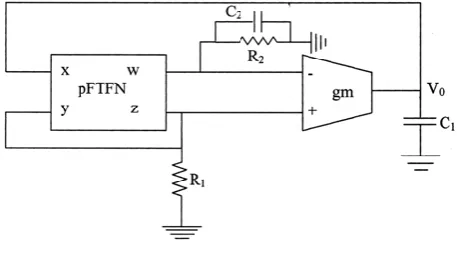
The positive FTFN can be characterized by the port relations with vx =vy, ix =iy = 0 and iw =iz.
Fig. 1 The circuit for the Oscillator The circuit above is the circuit for producing the oscillations required in the circuit.
III.DESIGN ISSUE WITH OSCILLATOR
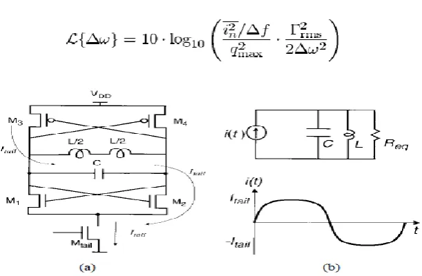
Due to their relatively good phase noise, ease of implementation, differential operation, cross-coupled inductance capacitance (LC) oscillators play an important role in high-frequency circuit design . In thispaper, the time-variant phase-noise model of will be applied toanalyse these oscillators. A simple expression for the tank amplitude is first obtained. The effect of different noise sources in such oscillators is then investigated, and methods for exploiting the cyclo stationary properties of noise are shown. New design implications arising from this approach and experimental results are given. A differential LC oscillator using spiral inductors is demonstrated that dissipates 6 mW of power while running at 1.8 GHz, with a phase noise of 121 dB/Hz at 600-kHz offset.
A. Tank Amplitude
Copyright to IJAREEIE www.ijareeie.com 1924 Fig 2 (a) Current flows when the stage is switched to one side. (b) Differential equivalent circuit
It is the power spectral density of the current where it is the rms value of the impulse noise, sensitivity function associated with that noise source, qmax is the maximum signal charge swing, and delta w is the offset frequency from the carrier.
A simple expression for the tank amplitude can be obtained assuming that the current in the differential stage switches quickly from one side to another. Fig. 2(a) shows the current flowing in the complementary cross-coupled differential LC oscillator [3] when it is completely switched to one side. As the tank voltage changes, the direction of the current flow through the tank reverses. The differential pair thus can be modeled as a current source switching between and in parallel with a resistance±inductance±capacitance(RLC) tank, as shown in Fig. it is the equivalent parallel resistance of the tank.
B. Rectangular Current Waveform
At high frequencies, the current waveform may be approximated more closely by a sinusoid due to finite switching time and limited gain. In such cases, the tank amplitude can be better approximated as
ISSN (Print) : 2320 – 3765 ISSN (Online): 2278 – 8875
I
nternational
J
ournal of
A
dvanced
R
esearch in
E
lectrical,
E
lectronics and
I
nstrumentation
E
ngineering
(An ISO 3297: 2007 Certified Organization) Vol. 4, Issue 4, April 2015
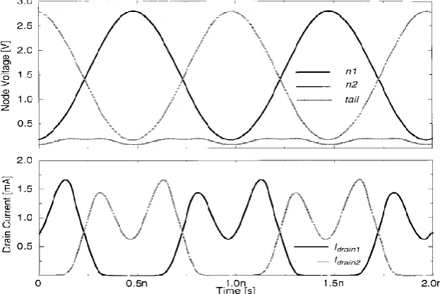
Copyright to IJAREEIE www.ijareeie.com 1925 Fig. 3 Simulated voltages and currents in the current-limited regime
Note that 3.2 loses its validity as the amplitude approaches the supply voltage because both NMOS and PMOS pairs will enter the triode region at the peaks of the voltage. Also the tail NMOS transistor may spend most (or even all) of its time in the linear region. This behavior can be seen in the simulated voltages and currents shown in Fig. 3.3 The tank voltage will be clipped at Vdd by the PMOS transistors and at ground by the NMOS transistors. Therefore, for the oscillator of Fig. 3(a), the tank voltage amplitude does not significantly exceed Vdd Note that since the tail transistor is in the triode region, the tail current does not stay constant. Thus, the drain-source voltage of the differential NMOS transistors can drop significantly, resulting in a large drop in their drain current, as shown in Fig. 3 This region of operation is known as the voltage-limited regime. Fig. 3 shows the simulated tank voltage amplitude as a function of tail current for three different values of VddAs can be seen, the tank amplitude is proportional to the tail current in the current-limited region, while it is limited by Vdd in the voltage-limited regime.
Copyright to IJAREEIE www.ijareeie.com 1926 III.DESIGNOFCURRENTMODESINUSOIDALOSCILLATOR
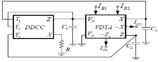
This paper presents a current-mode quadrature oscillator using differential different current conveyor (DDCC) and voltage differencing transconductance amplifier (VDTA) as active elements. The proposed circuit is realized from a non-inverting lossless integrator and an inverting second order low-pass filter. The oscillation condition and oscillation frequency can be electronically/orthogonally controlled via input bias currents. The circuit description is very simple, consisting of merely 1 DDCC, 1VDTA, 1 grounded resistor and 3 grounded capacitors. Using only grounded element, the proposed circuit is then suitable for IC architecture. The proposed oscillator has high output impedance which is easy to cascade or dive the external load without the buffer devices. The PSPICE simulation results are depicted, and the given results agree well with the theoretical anticipation. The power consumption is approximately 1.76mW at ±1.25V supply voltages.
A.Design using DDDC
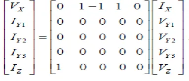
A third order currentmode oscillator, based on DDCC and VDTA. The features of the proposed circuits are that: the oscillation condition can be adjusted independently from the oscillation frequency by electronic method. The circuit construction consists of 1 DDCC, 1 VDTA, 1 grounded resistor and 2 grounded capacitors. The PSPICE simulation results are shown;the electrical behaviours of the ideal DDCC are represented by the following hybrid matrixes which are in correspondence with the theoretical analysis.
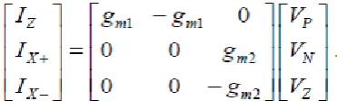
Fig. 4 Matrix representations of the parameters
The symbol and the equivalent circuit of the DDCC are illustrated in Fig. 5(a) and (b), respectively.
B. Design using VDTA
ISSN (Print) : 2320 – 3765 ISSN (Online): 2278 – 8875
I
nternational
J
ournal of
A
dvanced
R
esearch in
E
lectrical,
E
lectronics and
I
nstrumentation
E
ngineering
(An ISO 3297: 2007 Certified Organization) Vol. 4, Issue 4, April 2015
Copyright to IJAREEIE www.ijareeie.com 1927 Fig. 5 DDCC (a) Symbol (b) Equivalent circuit
If the VDTA is realized using CMOS technology, gm1 and gm2 can be respectively written as
Here k is the physical transconductance parameter of the CMOS transistor. IB1 and IB2 are the bias current used to control the gm1 and gm2, respectively.
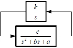
Copyright to IJAREEIE www.ijareeie.com 1928 Fig. 7 Block diagram for design of proposed oscillator
C.General structure of 3rd Oscillator
The oscillator is designed by cascading an inverting second order low-pass filter and the lossless integrators as systematically shown in Fig. 6. From block diagram in Fig. 7, we will receive the characteristic equation as
The condition of oscillation (OC) and frequency of oscillation (FO) can be written as
And
From above Equation, if a = c, the oscillation condition and oscillation frequency can be adjusted independently, which are the oscillation condition can be controlled by b and k, while the oscillation frequency can be tuned by a.
D.Structure of proposed Oscillator
The completed 3rd current-mode quadrature oscillator is shown in Fig. 7. The condition of oscillation and frequency of oscillation can be written as
ISSN (Print) : 2320 – 3765 ISSN (Online): 2278 – 8875
I
nternational
J
ournal of
A
dvanced
R
esearch in
E
lectrical,
E
lectronics and
I
nstrumentation
E
ngineering
(An ISO 3297: 2007 Certified Organization) Vol. 4, Issue 4, April 2015
Copyright to IJAREEIE www.ijareeie.com 1929 Fig. 8 Proposed Current-Mode Oscillator
If m1 B1 g = kI, m2 B2 g = kIand 1 2 3 C = C = C = C, the condition of oscillation and frequency of oscillation can be rewritten as
And
It is obviously found that, the condition of oscillation and frequency of oscillation can be adjusted independently, which are the oscillation of oscillation can be controlled by settingIB2, while the frequency of oscillation can be tuned by setting IB1. From the circuit in Fig. 8, the current transfer function from Io1 to Io2 is
For sinusoidal steady state, becomes
The phase difference φ between Io1 and Io2 is φ = -90° ensuring that the currents Io2 and Io1 are in quadrature.
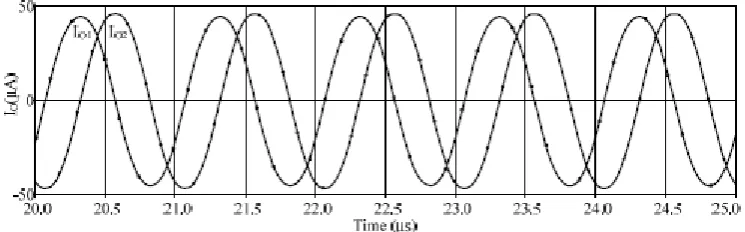
E .Output of proposed Oscillator
Copyright to IJAREEIE www.ijareeie.com 1930 Fig. 9 Internal construction of the CMOS DDCC
Fig. 10 Internal construction of the CMOS VDTA
ISSN (Print) : 2320 – 3765 ISSN (Online): 2278 – 8875
I
nternational
J
ournal of
A
dvanced
R
esearch in
E
lectrical,
E
lectronics and
I
nstrumentation
E
ngineering
(An ISO 3297: 2007 Certified Organization) Vol. 4, Issue 4, April 2015
Copyright to IJAREEIE www.ijareeie.com 1931 F. Practical Design of Proposed Circuit
Fig. 12 Practical Design of Proposed Circuit
III. RESULTS
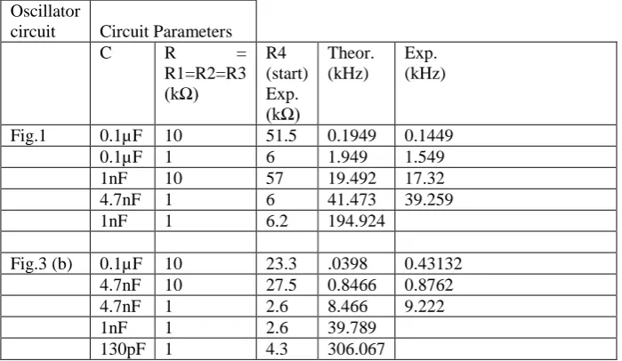
The confirm the theoretical analysis, the proposed SCRO circuit was simulated using one PFTFN and one OTA. The PFTFNwas constructed with two ad844 ic’s OF Analogue devices inc. and for OTA commercially available IC 3080 was used. The supply voltages were taken as +_15V dc. The passive component were selected as C1=0.01uf, C2 as 0.011uf, R2 as 20 Kohm and gm as 0.5 S. The value of C2 should be equal to 0.01uf, however in spice simulation it has been taken slightly higher i.e. equal to 0.011uf to make the s-term negative in equation so as to get sustained oscillations. It is an established practice in literature using the spice simulation method to verify the results.
The result which is obtained with the help of simulation contains different sections, of all the sections only the parameters obtained in the final report are shown.
Table 5.1 Results for the output obtained
Oscillator circuit
Circuit Parameters
C R =
R1=R2=R3 (kΩ) R4 (start) Exp. (kΩ) Theor. (kHz) Exp. (kHz)
Fig.1 0.1µF 10 51.5 0.1949 0.1449 0.1µF 1 6 1.949 1.549 1nF 10 57 19.492 17.32 4.7nF 1 6 41.473 39.259
1nF 1 6.2 194.924
Fig.3 (b) 0.1µF 10 23.3 .0398 0.43132 4.7nF 10 27.5 0.8466 0.8762 4.7nF 1 2.6 8.466 9.222
1nF 1 2.6 39.789
Copyright to IJAREEIE www.ijareeie.com 1932 OUTPUT OF RESULTS
IV.CONCLUSION
In this work an electronically tunable current-mode quadrature sinusoidal oscillator enabling independent current control of oscillation frequency and oscillation condition is realized employing three CDTAs and two grounded capacitors. The proposed circuit is canonical and capable of simultaneously providing two explicit quadrature current outputs. The non-ideal and sensitivity analyses of the circuit have been carried out, and the circuit exhibits a low sensitivity performance.
ISSN (Print) : 2320 – 3765 ISSN (Online): 2278 – 8875
I
nternational
J
ournal of
A
dvanced
R
esearch in
E
lectrical,
E
lectronics and
I
nstrumentation
E
ngineering
(An ISO 3297: 2007 Certified Organization) Vol. 4, Issue 4, April 2015
Copyright to IJAREEIE www.ijareeie.com 1933
REFERENCES
[1] E. H. Nordholt, ―Extending op amp capabilities by using a currentsourcepower supply,‖ IEEE Trans. Circuits Syst., vol. CAS-29, pp.411–414, June 1982.
[2] R. Prokop, V. Musil, ―New modern circuit block CCTA and some its applications,‖ The Fourteenth International Scientific and Applied Science Conference - Electronics ET’2005, Book 5. Sofia: TU Sofia, pp. 93-98, 2005.
[3] J. H. Huijsing and J. De Korte, ―Monolithic nullor—A universal activenetwork element,‖ IEEE J. Solid-State Circuits, vol. 12, pp. 59–64, Feb.1977.
[4] M. Higashimura, ―Realization of current-mode transfer function usingfour-terminal floating nullor,‖ Electron. Lett.,vol. 27, pp. 170–171, Jan.1991.
[5] J. H. Huijsing, ―Operational floating amplifier,‖ Proc. Inst. Elect. Eng.,vol. 137, pt. G, pp. 131–136, Apr. 1990. [6] R. Senani, ―A novel application of four-terminal floating nullors,‖ Proc.IEEE, vol. 75, pp. 1544–1546, Nov. 1987.
[7] A. Uygur and H. Kuntman ―CDTA-Based quadrature oscillator design,‖ in Proc. 14th European Signal processing conference (EUSIPCO
2006), September 4-8, 2006.
[8] M. Higashimura, ―Current-mode allpass filter using FTFN withgrounded capacitor,‖ Electron. Lett., vol. 27, pp. 1182–1183, June 1991. [9] S.-I. Liu, ―Cascadable current-mode filters using single FTFN,‖ Electron.Lett., vol. 31, pp. 1965–1966, Nov. 1995.
[10] S.-I. Liu and J.-L. Lee, ―Insensitive current/voltage-mode filters usingFTFN’s,‖ Electron. Lett., vol. 32, pp. 1079–1080, June 1996.
[11] N. A. Shah, S. Z. Iqbal, and M. Quadri, ―Current-mode Band-pass Filter Using A Single CDTA,‖ J. of Active and Passive Electronic Devices, vol. 4, pp. 1–5, 2009.
[12] M. T. Abuelma’atti, ―Cacadable current-mode filters using singleFTFN,‖ Electron. Lett., vol. 32, pp. 1457–1458, Aug. 1996.
[13] Jaikla, W., Siripruchyanun, M. ―CCCDTAs-based versatile quadrature oscillator and universal biquad filter‖. In Proc.of 2007 ECTI conference, Thailand, p. 1065-1068, 2007.
[14] U. Cam, A. Toker, O. Cicekoglu, and H. Kuntman, ―Current-mode high output-impedance sinusoidal oscillator configuration employing single FTFN,‖ Analog Integrated Circuits and Signal Proc., pp. 231-238, vol. 24, 2000.
[15] M. T. Abuelma’atti and H. A. Al-Zaher, ―Current-mode sinusoidal oscillators Using Single FTFN,‖ IEEE Trans. Circuits and Systems-II: Analog and Digital Signal Proc., vol. 46, pp. 69- 74, 1999.
[16] S. S. Gupta and R. Senani, ―Realisation of current-mode SRCOs using all grounded passive elements,‖ Frequenz, vol. 57, pp. 26-37, 2003. [17] M.T. Abuelma’atti, ―Grounded capacitor current-mode oscillator using single current follower,‖ IEEE Trans. Circuits and Systems-I:
Fundamental Theory and Applications, vol. 39, pp. 1018-1020, 1992.
[18] P. Prommee, K. Dejhan, ―An integrable electronic-controlled quadrature sinusoidal oscillator using CMOS operational transconductance amplifier,‖ International Journal of Electronics, vol. 89, pp. 365-379, 2002.
BIOGRAPHY
Copyright to IJAREEIE www.ijareeie.com 1934 DharamVir received the M.Tech Degree form MDU Rothak (Haryana) and B.E Degree in Electronics and Communication Engg. From JamiaMilliaIslamia (Central University), New Delhi 2008, 2004 respectively. In 1989 he started his carrier as R&D Engineer in the field of computers and networking. Since 1992 he is part of YMCA University of Science & Technology and presently working as Head of Section (Electronics & Inst. Control) in the Department of Electronics Engineering.