Available online:
http://edupediapublications.org/journals/index.php/IJR/
P a g e | 1919Design of Efficient Binary Comparators
in Quantum-Dot Cellular Automata
Mr. S.Madhavi
1, J.
RAMAKRISHNA
21
Associate professor, Department of ECE, Adams engineering College, Khammam Telangana.
2
M-Tech Student, Department of ECE, Adams engineering College, Khammam Telangana.
Abstract—Quantum-dot cellular automata (QCA) is one of the few alternative computing platforms that has the potential
to be a promising technology because of higher speed, smaller size, and lower power consumption in comparison with CMOS technology. This letter proposes an optimized full comparator for implementation in QCA. The proposed design is compared with previous works in terms of complexity, area, and delay. In comparison with the best previous full comparator, our design has 64% and 85% improvement in cell count and area, respectively. Also, it is implemented with only one clock cycle. The obtained results show that our full comparator is more efficient in terms of cell count, complexity, area, and delay compared to the previous designs. Therefore, this structure can be simply used in designing QCA-based circuits.
I. Introduction
In the last few decades, scaling the feature size and increasing the processing power have been successfully achieved by conventional lithography based on VLSI technology. However, it seems that even by decreasing the transistor sizes, some problems such as high power consumption and difficulties in feature size reduction cannot be ignored. Research predicts that CMOS technology may hit physical scaling limits in 2012 and will be superseded by some emerging technologies. Nanotechnology is an alternative to these problems, and the ITRS report summarizes several possible technology solutions. Relying on the unique properties of electronic devices at nanoscale feature size, nanotechnology opens up new horizons for computing systems and devices. Quantum-dot cellular automata (QCA) is an emerging technology that offers a revolutionary approach to computing at nano-level. QCA proposed by Lent and others created general computational functionality at
the nanoscale by controlling the position of a single electron. This technology promises extra low power, high speed, and extremely dense circuits. Using QCA technology for the implementation of logic circuits not only increases the clock frequency of logic circuits and decreases the size of these circuits, but also reduces the power consumption of these circuits. Furthermore, the circuits based on the QCA have the ability of highly parallel processing. One of the basic digital devices, and probably a vital part of many modern computing
platforms, is the comparator. Previously, comparator designs were examined for implementation with QCA technology. In this letter, we propose an optimized full comparator based on QCA implementation working with only 4 clock phases. This design requires a minimum number of cells and area allocations as compared to the previous works.
II. QCA Basis
Available online:
http://edupediapublications.org/journals/index.php/IJR/
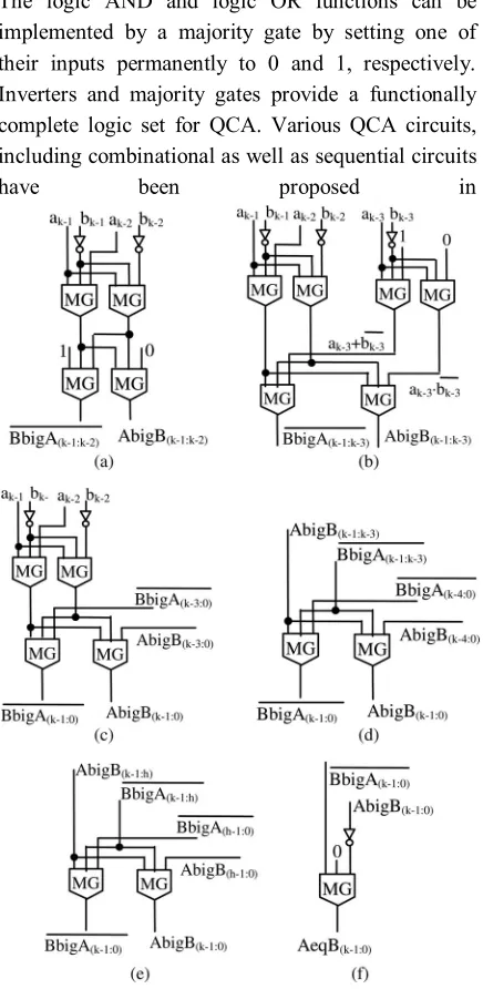
P a g e | 1920 Fig. 1. QCA-based comparators presented inpropagates from input to output because of the electrostatic interactions between the cells. There are two kinds of QCA wires as shown in Fig. 1(b) and Fig. 1(c). One is a binary wire implemented with the cells of 90º orientation, and the other is an inversion chain implemented with the cells of 45º orientation. Each cell in the inversion chain takes on the opposite polarization of its neighbors. Fig. 1(d) shows the QCA multilayer crossing structure. Multilayer crossing is constructed by adding more layers. Any QCA circuit can be efficiently built using only majority gates and inverters.
The simplest structure of the inverter, shown in Fig. 1(e), is usually formed by placing the cells only with their corners touching. In Fig. 1(f), the 45º displacement in the two lines of merging cells produces the complement of the input signal. Figure 1(g) shows the gate symbol of the inverter. The fundamental logic gate for QCA is the 3-input majority gate composed of 5 cells. Figures 1(h) and 1(i) show the QCA layout and its gate symbol, respectively. Assuming that the inputs are a, b, and c, the logic function of 3-input majority gate can be expressed as
f a.b b.c a.c M ( a , b , c). (1)
The logic AND and logic OR functions can be implemented by a majority gate by setting one of their inputs permanently to 0 and 1, respectively. Inverters and majority gates provide a functionally complete logic set for QCA. Various QCA circuits, including combinational as well as sequential circuits
have been proposed in
Available online:
http://edupediapublications.org/journals/index.php/IJR/
P a g e | 1921 C2.Fig. 3. Novel 32-bit CB full comparator.
III. Design Approach
Comparator is one of the important components in logic design. Comparators are used in central processing units (CPUs) and microcontrollers. If we assume that the
inputs are A and B and the outputs are OA=B, OA>B,
and OA<B, the logical functions of the half comparator
can be expressed as
OAB A. B,
OAB A .B, (2)
OAB OAB . OAB .
Also, the equations for a full comparator are given by
OAB A. B.C,
OAB A.B.C, (3)
OAB OAB . OAB ,
where for an n-bit full comparator, the output OA=B of one stage is fed directly to the input C of the next stage. The logic diagram of a full comparator is presented in Fig. 2(a). Equations for a full comparator realized with majority gates and inverters are shown below
OAB M (M (A, B, − 1), −1,C),
OAB M (M (A, B, − 1), −1,C), (4)
OAB M (OAB , OAB , −1).
IV. Results and Discussion
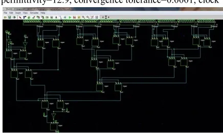
The QCA implementation of the proposed full comparator is simulated by the QCADesigner tool [14]. The following parameters are used for a bistable
approximation [14]: cell size=18 nm×18 nm, number of samples=12,800, radius of effect=65 nm, relative permittivity=12.9, convergence tolerance=0.0001, clock
Figure 4.Schematic diagram of 32-bit comparator.
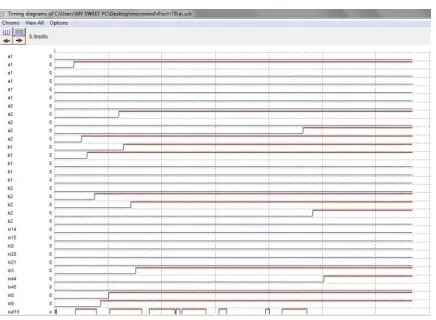
high=9.8e–22J, clock low=3.8e–23J, clock amplitude factor=2, layer separation=11.5 nm, and maximum iterations per sample=100. Also, the diameter of the quantum dot is 5 nm and the cell distance is 2 nm. The input and output waveforms for the proposed full comparator are shown in Fig. 3. Table 1 shows the comparison between the proposed full comparator and the previous ones, where HC, FC, and SC stand for half comparator, full comparator, and serial comparator, respectively. As shown in Table 1, our full comparator has resulted in significant improvements in terms of area, complexity, and delay.
Fig.5. Layout diagram.
Available online:
http://edupediapublications.org/journals/index.php/IJR/
P a g e | 1922 Fig 7.Timig diagram for 32-bit comparator.In comparison to the previous works that have used coplanar crossing, we used a two-layer layout in our design. We have designed the logical structures using a 2-cell inverter instead of a 7-cell inverter. By applying this method, the hardware requirements for a QCA design can be reduced. Also, we have done part of the calculation in layer two to obtain the outputs that make the proposed layout an efficient design with a minimum number of cells, smaller size, and less delay. These methods can be applied to other QCA circuits, such as Full Adder, to reduce the hardware requirements for a QCA design.
V. Conclusion
In this letter, an optimized QCA full comparator was proposed. The proposed comparator is simulated using the QCADesigner tool, and the simulation results show that the logical function of the designed circuit is correct. The optimized QCA full comparator shows improvement in terms of area, cell count, and delay. In comparison with the best previous full comparator, our design has 64% and 85% improvement in the cell count and the area, respectively. Also, our comparator is faster than previous ones. Therefore, the implementation of this design may lead to the efficient use of calculative units in various applications, which may be used as a basic building block of a general purpose nano processor.
REFERENCES
[1] C. S. Lent, P. D. Tougaw, W. Porod, and
G. H. Bernestein, “Quantum
cellular automata,”
Nanotechnology
, vol. 4,
no. 1, pp. 49–57, 1993.
[2] M. T. Niemer and P. M. Kogge,
“Problems in designing with QCAs: Layout
= timing,”
Int. J. Circuit Theory Appl.
, vol.
29, pp. 49–62, 2001.
[3]
G.
H.
Bernstein,A.
Imre,V.Metlushko,A.Orlov, L. Zhou, L.
Ji,G. Csaba,
and W. Porod, “Magnetic QCA systems,”
Microelectron. J.
, vol. 36,
pp. 619–624, 2005.
[4] J.Huang and F. Lombardi,
Design and
Test of DigitalCircuits by Quantum-
Dot Cellular Automata
. Norwood, MA,
USA: Artech House, 2007.
[5] W. Liu, L. Lu, M. O’Neill, and E. E.
Swartzlander Jr., “Design rules for
quantum-dot cellular automata,” in
Proc.
IEEE Int. Symp. Circuits Syst.
(ISCAS)
, Rio De Janeiro, Brazil, May 2011,
pp. 2361–2364.
[6] K. Kim, K. Wu, and R. Karri, “Towards
designing robust QCA architectures
in the presence of sneak noise paths,” in
Proc. IEEE Design,
Automation
Test
Eur.
Conf.
Exhib.
(DATE)
,Munich, Germany,Mar. 2005,
pp. 1214–1219.
[7] K. Navi, M. H. Moaiyeri, R. F. Mirzaee,
O. Hashemipour, and
B. M. Nezhad, “Two new low-power full
adders based on majority-not
gates,”
Microelectron. J.
, vol. 40, pp. 126–
130, 2009.
Available online:
http://edupediapublications.org/journals/index.php/IJR/
P a g e | 1923quantum-dot cellular automata,”
IEEE
Trans. Nanotechnol.
, vol. 6, no. 3,
pp. 374–383, May 2007.
[9] H. Cho and E. E. Swartzlander Jr.,
“Adder and multiplier design in
quantum-dot cellular automata,”
IEEE
Trans. Comput.
, vol. 58, no. 6,
pp. 721–727, Apr. 2009.
[10] V. Pudi and K. Sridharan, “Efficient
design of a hybrid adder in quantumdot
cellular automata,”
IEEE Trans. VLSI Syst.
,
vol. 19, no. 9, pp. 1535–
1548, Jul. 2011.
[11] M. Gladshtein, “Quantum-dot cellular
automata serial decimal adder,”
IEEE Trans. Nanotechnol.
, vol. 10, no. 6,
pp. 1377–1382, Nov. 2011.
[12] V. Pudi and K. Sridharan, “Low
complexity design of ripple carry and
Brent-Kung adders in QCA,”
IEEE Trans.
Nanotechnol.
, vol. 11, no. 1,
pp. 105–119, Jan. 2012.
[13] S. Perri and P. Corsonello, “New
methodology for the design of efficient
binary circuits addition inQCA,”
IEEE
Trans.Nanotechnol.
, vol. 11, no. 6,
pp. 1192–1200, Nov. 2012.
[14] V. Pudi and K. Sridharan, “New
decomposition theorems on majority
logic for low-delay adder designs in
quantum dot cellular automata,”
IEEE Trans. Circuits Syst. II: Exp. Brief
,
vol. 59, no. 10, pp. 678–682,
Oct. 2012.
[15] H. Cho and E. E. Swartzlander Jr.,
“Serial parallel multiplier design in
quantum-dot cellular automata,” in
Proc.
IEEE Symp. Comput. Arithmetic
,2007
Mrs S. Madhavi hailed
from
Khammam(Dist.)
born
on
18th
August 1976.She received
B.Ein
Electronics
and
Communication
Engineering from SRKR
Engineering
College,
Bhimavaram, Andhra University, AP. She
received M.Tech in Digital Systems and
Computer
Electronics
from
JNTU
Anantapur, AP, India. Her research interests
include Analog VLSI Design, Digital VLSI
Design and Low Power Memory Design and
Fault Diagnosis. Presently she is working as
Associate.Prof
in
ADAMS
engineeringCollege, Paloncha, Khammam
(Dist). She is having 15 years experience in
teaching field on Digital and VLSI related
areas.
mailid:
[email protected]
Mr. J.RAMAKRISHNA M.TECH (VLSI system design ) PURSUING In Adam’s Engineering College, Paloncha, Khammam DIST,
TELANGANA, INDIA.