A RIDGE WAVEGUIDE FOR THERMO-OPTIC APPLICATION
A. M. Al-Hetar, A. S. M. Supa’at, and A. B. Mohammad
Photonics Technology Center (PTC) Faculty of Electrical Engineering Universiti Teknologi Malaysia (UTM) 81310 Johor, Malaysia
Abstract—A thermal analysis and structure of a ridge single mode waveguide with a metal heater are presented. The steady-state temperature increases linearly and the thermal response becomes slower at the same power consumption, when the under-etched depth in the lower cladding increases. When the upper cladding thickness decreases, the thermal response becomes faster. This shows that a thinner upper cladding and a deeper etching are preferred to achieve a faster thermal response and lower power consumption, respectively. The numerical simulation also shows that the power consumption of the present ridge waveguide is almost a third of that for conventional one and the response time is half of that of the conventional one.
1. INTRODUCTION
Integrated optical device based on planar lightwave circuits (PLC) technology have attracted much attention due to their excellent performances and compact size. There are many kinds of optical waveguide based on different materials and structures, such as InP, SiO2, etc. [1]. For passive PICs, the SiO2 buried waveguide is one of the most popular choices due to its outstanding advantages such as low cost, small propagation loss, and good matching to a single mode fiber [2, 3]. On the other hand, it is required a relatively large separation (>20µm) between two parallel SiO2 buried waveguide to avoid the evanescent coupling between them. This limits its application for achieving large-scale PICs with high integration densities. In addition to that, the air trench between two parallel buried waveguides
is required to limit a thermal coupling if one of them is heated [4]. For active devices, the devices are operated using such as thermo-optic effect, which is weak in SiO2 based materials and results in high power consumption. On the other hand, polymer materials have a large thermo-optic (TO) coefficient (which is about 10 times greater than that of SiO2).
In this work, we present a polymer ridge waveguide with a metal heater, which has a very simple fabrication process. In this case, only one lithography process is necessary and no heat insulation grooves are needed due to the ridge structure. Compared with the conventional buried waveguide, lower power consumption and faster response can be achieved in the ridge waveguide with a metal heater. In order to give a theoretical evaluation for the present ridge waveguide with a metal heater, thermal modeling according to the heat conduction theory is established. The effects of the structure parameters on the thermal characteristics at the ridge waveguide are studied.
2. STRUCTURE AND THERMAL MODELING
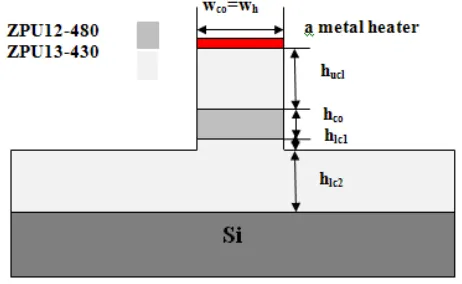
The cross-section of the present ridge waveguide with a metal heater is shown in Fig. 1. When the electrical current flows through the metal heater, the heater with resistance will produce Joule heat, which will go through the upper cladding layer to the waveguide core. The change of refractive index is dependent on the thermal coefficient of materials dn/dT and the change of temperature ∆T [5].
Figure 1. The cross section of the ridge waveguide with a metal heater.
response of the waveguide, the equation to be solved is the heat transfer Fourier’s equation in transient condition with constant thermal conductivity [6, 7].
ρ·cp·
∂T
∂t = K· ∇
2T+Q(x, y, z, t) (1)
T(x, y, z, t)t=0 = T0 (2)
where K is the thermal conductivity (W·m−1◦C−1); ρ is the material density (Kg·m−3); cρ is the specific heat of material (J·Kg−1·◦C−1) and Qis the thermal energy generated inside unit volume during unit time (W·m−3). The corresponding boundary conditions at different interfaces are given as following:
−K∂T
∂s = 0 (3)
−K∂T ∂s =
Q
A (4)
−K1
∂T
∂s = −K2 ∂T
∂s (5)
Equation (3) describes the mechanism of heat transfer which is conduction, ignoring the convection heat transfer [3]. The boundary condition in Eq. (1) states that lateral and top surfaces are adiabatic, while Eq. (2) assigns affixed temperature of the bottom and considers Silicon a perfect heat sink [5]; T0 = 25◦C is the room temperature of the air. Eq. (4) is the heat flux boundary condition at the heater/dielectric interface where Q is the heater power and A is the contact area of heater. In case that the thermal conductivity of upper cladding, core, and lower cladding is different, Eq. (5) will be used to describe the continuity of heat flux at the interfaces.
In this work, we used a simple and accurate Finite Element Method (FEM) to solve the above differential equations and find the response of heating at transient and steady-state.
3. SIMULATION RESULTS
A 4µm×1.5µm core is chosen, the under-etching depth hlc1 = 1µm, and the total thickness of the insulator layer htol = 6µm (i.e., htolc =
thin up-cladding is desired to obtain a fast thermal conduction from the heater to the core. Here we choosehucl= 5µm as a trade-off.
In the following part, the thermal behavior of the ridge waveguide is analyzed which based on the thermal modeling described in the previous section. The temperature of the center point in the core is used to evaluate the thermal characteristics. The polymeric materials used in the modeling and simulation are ZPU series from ChemOptics Co. Ltd. The refractive indexes of the polymers used for the core and cladding are 1.48 and 1.43, respectively. The thermal properties of polymer are as following, the thermal conductivity K = 0.2 (W· m−1·◦C−1), density of polymer ρ = 1.2×10³(Kg·m−3), and specific heat or heat capacitycp = 1.3×10³(J·Kg−1·◦C−1). For the heater, the lengthLh, widthwh, and thicknessth are 100µm, 4µm, and 0.4µm, respectively.
The temperature response was calculated when the heater power
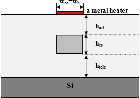
Q is set to 1 mW, 1 mW, 1.5 mW, 2 mW, 2.5 mW, and 3 mW. For comparison, the buried waveguide with a metal heater as shown in Fig. 2 is also analyzed at the same heater power. In the buried waveguide, the thickness of core becomes 1.5µm (square core) and the rest of dimensions equal of that in the ridge waveguide.
Figure 2. The cross section of the buried waveguide with a metal heater.
(a)
(b)
(c)
power from 1 mW to 3 mW. The steady-state core temperature and the heating rise time are shown in Figs. 3(b) and (c), where the line with red dots and blue squares are the ridge and buried waveguides, respectively.
Figure 3 shows that the core temperature of both structures rises linearly with the heater power, while the rise time keeps unchanged. When the power is 1 mW, 1.5 mW, 2 mW, 2.5 mW, and 3 mW, the core temperature for the ridge waveguide reaches about 78◦C, 104◦C, 130◦C, 156◦C, and 182◦C, respectively, while the core temperature for the conventional buried waveguide reaches about 46◦C, 57◦C, 67◦C, 78◦C, and 88◦C, respectively. In the Figs. 3(b) and (c), it is clear that the temperature in the ridge waveguide rises more quickly than that in
(a)
(b)
(a)
(b)
Figure 5. (a) The core temperature response for different values of under-etching thickness, and (b) the steady-state core temperature and rise time for different values of under-etching thickness.
the conventional buried waveguide, and the power consumption of the present ridge waveguide is almost a third of that for the conventional one. On the other hand, the heating rise time on the ridge waveguide is 0.8 ms, which is half of that for the conventional one. Therefore, the present ridge waveguide with a metal heater is much more power-saving and much faster than the conventional buried waveguide.
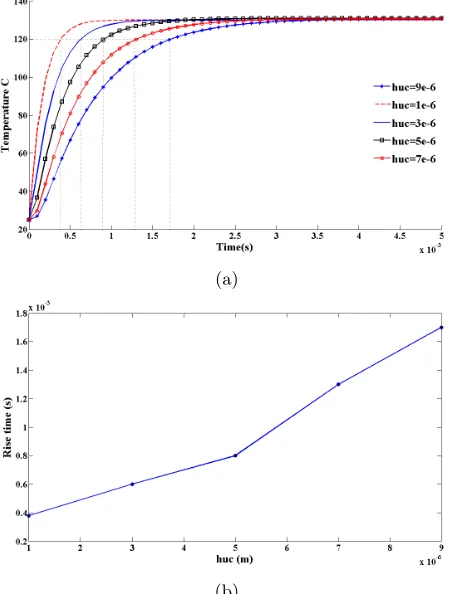
In this part, the thermal characteristics of a ridge waveguide with different geometrical parameters are considered. Fig. 4 shows the core temperature response and the rise time for different values of the up-cladding thickness (hucl= 1µm, 3µm, 5µm, 7µm, and 9µm). Where
up-cladding thickness. However, the heating rise time is quite different. When,huclincreases from 1µm to 9µm, the rise time increases almost linearly from 0.4 ms to 1.7 ms. This indicates that a shorter response time requires a thinner up-cladding layer. However, the up-cladding layer must be thick enough to reduce the absorption loss due to the metal heater. In this design and materials, hucl= 5µm is chosen.
Figure 5 shows the core temperature responses for different values of the under-etching thickness (hlc1), when Q = 2 mW, hucl = 5µm, andhlc1+hlc2= 6µm, and the steady-state core temperature and rise time in Fig. 5(b) when the under-etched depth hlc1 ranges from 1µm to 5µm.
It is clear that the steady-state core temperature increases linearly while the response becomes slower when under-etched depth hlc1 increases from 1µm to 5µm. Therefore, a large depth hlc1 is desired to get lower power consumption. On the other hand, for the case a shallower etching depthhlc1, a faster thermal response is obtained (i.e., shorter rise time). Here,hlc1 = 1µm andhucl= 5µm are chosen as a trade-off to achieve a fast heat response and low power consumption.
4. CONCLUSION
In this work, a ridge waveguide with a metal heater is presented. The fabrication process requires only one lithography process, which is simpler than that for a conventional buried waveguide with a metal heater. The thermal behavior of the present ridge waveguide has been analyzed according to the modeling based on the conduction theory. The numerical simulation results based on FEM have shown that the power consumption of the present ridge waveguide is almost a third of that for the conventional one and the response time is about half of that of the conventional one. In the end of this work, the effects of the structural parameter on the thermal characteristics are analyzed to achieve fast heat response and low power consumption. Therefore, the present ridge waveguide with a metal heater can be used for various thermo-optic devices, such as TO MZI, due to its good thermal performance.
ACKNOWLEDGMENT
REFERENCES
1. Kokubun, Y., Y. Hatakeyama, M. Ogata, and S. S. Zaizen, “Fabri-cation technologies for vertically coupled microring resonator with multilevel crossing busline and ultracompact-ring radius,” IEEE J. Sel. Topics Quantum Electron., Vol. 11, No. 1, 4–10, 2005. 2. Goebuchi, Y., T. Kato, and Y. Kokubun, “Fast and stable
wavelengthselective switch using double-series coupled dielectric microring resonator,”IEEE Photon. Technol. Lett., Vol. 18, No. 1, 538–540, 2006.
3. Al-hetar, A. M., I. Yulianti, A. S. M. Supa’at, and A. B. Moham-mad, “Thermo-optic multimode interference switches with air and silicon trenches,” Optics Communications, Vol. 281, 4653–4657, 2008.
4. Chao, F.-L., “Trench structure improvement of thermo-optic waveguides,” International Journal of Applied Science and Engineering, Vol. 5, No. 1, 1–5, 2007.
5. Dimeer, M. B. J., “Polymeric thermo-optic space switches for optical communication,”Optical Material, Vol. 9, 192–200, 1998. 6. Jaluria, Y. and K. E. Torrance, Computational Heat Transfer,
Second Edition, Taylor & Francis, NY, 2003.
7. Jensen, V. G. and G. V. Jeffreys, Mathematical Methods in Chemical Engineering, 2nd edition, Academic press, NY, 1977. 8. Nishihara, H., M. Haruna, and T. Suhara, Optical Integrated
Circuits, McGraw-Hill, NY, 1989.