© 2014, IJCSMC All Rights Reserved 500 Available Online atwww.ijcsmc.com
International Journal of Computer Science and Mobile Computing
A Monthly Journal of Computer Science and Information Technology
ISSN 2320–088X
IJCSMC, Vol. 3, Issue. 5, May 2014, pg.500 – 505
RESEARCH ARTICLE
Implementation of Reversible Sequential
Circuits Using Conservative Logic Gates
Dhaarinee.S
1, Rajeswaran.N
21PG Scholar, Department of ECE, SNS College of Technology, Coimbatore-35
2
Associate Professor, Department of ECE, SNS College of Technology, Coimbatore-35
[email protected];[email protected]
Abstract- Reversible circuits do not loose any information during computation. Reversible computation can be performed
using reversible gates like fredkin gate, feynmann gate and toffoli gate. It has unique output vector for each input vector and
has one to one mapping between the inputs and outputs. The existing system is designed using fredkin gate and they are
cascaded in series or parallel using the characteristic equation of each reversible gate. In the proposed system sequential
circuits like master slave flip-flop and edge triggered flip-flop are designed using toffoli gate which is universal in nature.
These circuits have less power dissipation and are used in applications like quantum computing, digital signal processing,
cryptography nanotechnology and testing. The circuit can detect stuck at fault using two test vectors 0 and 1.
Keywords - fredkin gate; quantum computing; toffoli gate; stuck at fault; reversible logic
I. INTRODUCTION
Reversible logic appears to be promising due to its wide applications in emerging technologies. Some of the
applications of reversible logic are quantum computing, quantum dot cellular automata, optical computing, Spintronics, DNA
computing, molecular computing and also in power-efficient nano computing. Reversible circuits are those circuits that do not
lose information during computation and reversible computation in a system can be performed only when the system comprises
of reversible gates. These circuits can generate unique output vector from each input vector, and there is a one-to-one mapping
between the input and the output vectors. In an irreversible gate information is physical and some minimum amount of energy is
© 2014, IJCSMC All Rights Reserved 501 A. Basic reversible gates
The basic reversible gates are those that create one to one mapping between inputs and outputs. The number of outputs
are equal to the number of inputs. These gates do not result in power dissipation and are conservative in nature. The basic
reversible gates are the conventional not gate, Feynman gate , Fredkin gate and Toffoli gate.
1)Feynman gate :It is a two input and two output gate implemented using the XOR function.
Fig 1 Feyman Gate
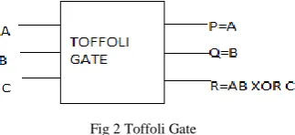
2)Toffoli gate: The Toffoli gate can be implemented by using the following equations.
Fig 2 Toffoli Gate
3) Fredkin gate: The Fredkin gate or controlled-swap gate, swaps the two inputs B and C if A is true.
Fig 3 Fredkin Gate II. SYSTEM MODEL
The design of master slave flip-flop and double edge triggered flip-flop are presented using fredkin gate in the existing
system
.A. Design of master-slave flip-flops using fredkin gate
In this design two latches namely negative enable slave latch and positive enable slave latch are cascaded as shown in
the Fig. 4.The master positive enable latch is designed using the characteristic equation Q+ = DE+ E’Q with clock = 1.The slave
negative enable latch is designed using the characteristic equation Q+ = DE’ + EQ.
© 2014, IJCSMC All Rights Reserved 502
The testable reversible D flip-flops has four control signals mC1, mC2, sC1 and sC2.mC1 and mC2 control the modes
for the master latch, while sC1 and sC2 control the modes for the slave latch. In the normal mode, when the design is working
as a master-slave flip-flop the values of the controls signals will be mC1=0 and mC2=1, sC1=0 and sC2=1.In the test mode, to
make the design testable with all 0s input vectors for any stuck-at-1 fault, the values of the controls signals will be mC1=0 and
mC2=0, sC1=0 and sC2=0. This will make the outputs mT1 and sT1 as 0 that results in breaking the feedback and the design
becomes testable with all 0s input vectors for any stuck-at-1 fault. To make the design testable with all 1s input vectors for any
stuck-at-0 fault, the values of the control signals will be mC1=1 and mC2=1, sC1=1 and sC2=1.This will result in outputs mT1
and st1 to have the value of 1 breaking the feedback and resulting in the design testable with all 1s input vectors for any
stuck-at-0 fault.
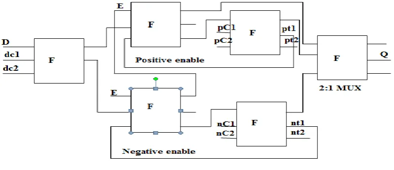
B. Design of double edge triggered flip-flops using fredkin gate
The double edge triggered flop stores input value at both positive and negative edges of the clock. The DET
flip-flop is designed by connecting the two latches, the positive enable and the negative enable in parallel rather than in series. In Fig
.5 the Fredkin gates labeled as 1 and 2 forms the positive enable D latch while the Fredkin gates labeled as 3 and 4 forms the
negative enable D latch.
Fig 5 Fredkin gate based double edge triggered flip-flop
In the negative edge triggered master-slave flip-flop when E=1 the clock is high, the master latch passes the input data
while the slave latch maintains the previous state. When E=0 the clock is low, the master latch is in the storage state while the
slave latch passes the output of the master latch to its output. The Fredkin gate labeled as 5 works as the 2:1 MUX and transfer
the output from one of these testable latches that is in the storage state to the output Q. In the design of testable reversible DET
flip-flop pC1 and pC2 are the controls signals of the testable positive enable D latch, while nC1 and nC2 are the control signals
of the testable negative enable D latch. Depending on the values of the pC1, pC2, nC1 and nC2 the testable DET flip-flops
works either in normal mode or in the testing mode. The normal mode of the DET flip-flop in which the pC1=0, pC2=1, nC1=0
and nC2=1.
In the test mode there are all 1 and all 0 mode. In the all 0s Test Vector as shown in Fig.5 at which the control signals
will have value as pC1=0, pC2=0, nC1=0 and nC2=0. The pC1=0 and pC2=0 help in breaking the feedback of the positive
enable D latch while the nC1=0 and nC2=0 help in breaking the feedback of the negative enable D latch. This makes the design
© 2014, IJCSMC All Rights Reserved 503
pC2=1, nC1=1 and nC2=1.The pC1=1 and pC2=1 help in breaking the feedback of the positive enable D latch, while the nC1=1
and nC2=1 help in breaking the feedback of the negative enable D latch. This makes the design testable by all 1s test vector for
any stuck-at-0 fault.
III.PROPOSED SYSTEM
The design of master slave flip-flop and double edge triggered flip-flop are presented using toffoli gate.
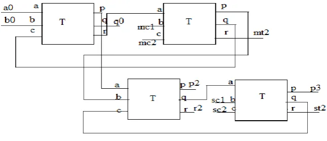
A. Design of testable master -slave flip-flops using toffoli gate
In this design two latches namely negative enable slave latch and positive enable slave latch are cascaded as shown in
the Fig.6.The master positive enable latch is designed using the characteristic equation Q+ = DE+E’Q with clock = 1.The slave
negative enable latch is designed using the characteristic equation Q+ = DE’ + EQ. The testable reversible D flip-flops has four
control signals mC1, mC2, sC1 and sC2.mC1 and mC2 control the modes for the master latch, while sC1 and sC2 control the
modes for the slave latch. In the normal mode, when the design is working as a master-slave flip-flop the values of the controls
signals will be mC1=0 and mC2=1, sC1=0 and sC2=1.
Fig 6 Toffoli gate based testable reversible master-slave D flip-flop
In the test mode, to make the design testable with all 0s input vectors for any stuck-at-1 fault, the values of the controls
signals will be mC1=0 and mC2=0, sC1=0 and sC2=0. This will make the outputs mT1 and sT1 as 0 that results in breaking the
feedback and the design becomes testable with all 0s input vectors for any stuck-at-1 fault. To make the design testable with all
1s input vectors for any stuck-at-0 fault, the values of the control signals will be mC1=1 and mC2=1, sC1=1 and sC2=1.This
will result in outputs mT1 and st1 to have the value of 1 breaking the feedback and resulting in the design testable with all 1s
input vectors for any stuck-at-0 fault.
B. Design of testable reversible double edge triggered flip-flops using toffoli gate
The DET flip-flop is designed by connecting the two latches, the positive enable and the negative enable in parallel
rather than in series as shown in Fig.7.Depending on the values of the pC1, pC2, nC1 and nC2 the testable DET flip-flops works
either in normal mode or in the testing mode. The normal mode of the DET flip-flop in which the pC1=0, pC2=1, nC1=0 and
nC2=1.The pC1=0, pC2=1 helps in copying the output of the positive enable D latch thus avoiding the fan out while the nC1=0
and nC2=1 helps in copying the output of the negative enable D latch thus avoiding the fan out. In the test mode there are all 1
© 2014, IJCSMC All Rights Reserved 504 Fig 7 Toffoli gate based Double Edge Triggered flip-flop in test mode
In the all 1s Test Vector at which control signals will have value as pC1=1, pC2=1, nC1=1 and nC2=1.This makes the
design testable by all 1s test vector for any stuck-at-0 fault. In the all 0s Test Vector at which the control signals will have value
as pC1=0, pC2=0, nC1=0 and nC2=0. This makes the design testable by all 0s test vector for any stuck-at-1 fault.
IV. SIMULATION RESULTS
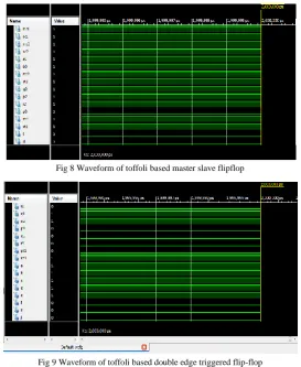
The simulation results for toffoli based master slave flip-flop that can detect stuck at 0 fault by setting all inputs to 1.
Fig 8 Waveform of toffoli based master slave flipflop
Fig 9 Waveform of toffoli based double edge triggered flip-flop
The simulation results for toffoli based double edge triggered flip-flop that can detect stuck at 0 fault by setting all
© 2014, IJCSMC All Rights Reserved 505 V. CONCLUSION
The reversible sequential circuits like master slave flip-flop and double edge triggered flip flop are designed using
fredkin gate and toffoli gate. These circuits have less power dissipation and are used in applications like quantum computing,
digital signal processing, cryptography nanotechnology and testing. The proposed reversible sequential designs are simulated
verilog HDL and the waveforms are presented. This work can also be extended to the design of counter and registers.
REFERENCES
[1] H.Thapliyal, N.Ranganathan and S.Kotiyal,”Design of testable reversible sequential circuits,” IEEE Trans.VLSI vol 21, no. 7,July 2013.
[2] H. Thapliyal and N. Ranganathan, “Design of reversible sequential circuits optimizing quantum cost, delay and garbage outputs,” ACM J.Emerg. Technol. Comput. Syst., vol. 6, no. 4, pp. 14:1–14:35, Dec. 2010.
[3] E. Fredkin and T. Toffoli, “Conservative logic,” Int. J. Theor. Phys.,vol. 21, nos. 3–4, pp. 219–253, 1982
[4] S. Mahammad and K. Veezhinathan, “Constructing online testable circuits using reversible logic,” IEEE Trans. Instrum. Meas., vol. 59,no. 1, pp. 101–109, Jan. 2010.