A 14-bit Hybrid Incremental Sigma-Delta/Cyclic
ADC for X-ray Linear Array Sensor
Yuze Niu 1,2, Yacong Zhang 1,2,*, Zhuo Zhang 1,2, Miaomiao Fan 1, Wengao Lu 1,2 and Zhongjian Chen 1,2 1 Key Laboratory of Microelectronic Devices and Circuits, Department of Microelectronics, Peking University, Beijing 100871, China; [email protected] (Y.N.); [email protected] (Z.Z.); [email protected] (M.F.);
[email protected] (W.L.); [email protected] (Z.C.)
2 Peking University Information Technology Institute (Tianjin Binhai), Tianjin 300452, China * Correspondence: [email protected]
Abstract—This paper presents a two-stage ADC based on pseudo-differential operational transconductance amplifier (OTA), which is designed for the readout circuit of X-ray linear array sensor. This hybrid ADC employs an incremental sigma-delta ADC and a cyclic ADC, achieving a good trade-off between accuracy and conversion speed. The two stages share the same hardware to reduce power consumption and die area. A common-mood feedback module is used to suppress the influence of charge injection, and the effectiveness is demonstrated by detailed theoretical analysis. A test chip of 14-bit ADC is fabricated in 0.35μm CMOS technology. The measured root mean square (RMS) value of DNL is 0.254 LSB, and the maximum value of INL is -0.776/+1.56 LSB. The measured effective number of bits (ENOB) is 13.43 bits.
Keywords—hybrid ADC; sigma-delta ADC; cyclic ADC; pseudo-differential OTA; X-ray sensor I. INTRODUCTION
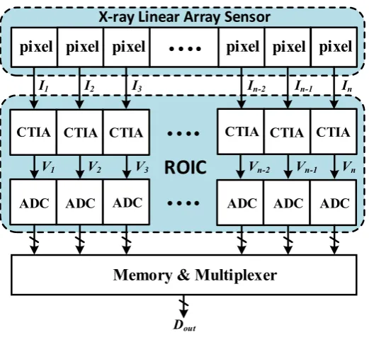
X-ray imaging system is widely used in many fields such as medical, industrial, and safety monitoring areas [1]. Readout Integrated Circuit (ROIC) of the X-ray sensor has a significant effect on signal-to-noise ratio of the system [2]. Since digital signal has strong resistance to interference, ROIC integrated with Analog-to-Digital Converter (ADC) is drawing more and more attention. There are many channels in the ROIC of X-ray linear array sensor, and it is a good choice to integrate an ADC in each channel to alleviate speed requirements for ADC. The architecture of the ROIC is shown in Fig. 1. The front-end circuit of the ROIC is called Capacitive Trans-Impedance Amplifier (CTIA), which is used to convert tiny current signal generated by the X-ray linear array sensor to analog voltage signal. The ADC in each channel of the ROIC should feature small die area, low power consumption, high resolution and moderate speed to realize good performance.
pixel pixel
pixel
….
pixel
pixel
pixel
CTIA
ADC ADC ADC ADC ADC ADC
Memory & Multiplexer
ROIC
I1 I2 I3 In-2 In-1 In
V1 V2 V3 Vn-2 Vn-1 Vn
CTIA CTIA
….
CTIA CTIA CTIA….
Dout
X-ray Linear Array Sensor
Fig. 1. ROIC of the X-ray linear array sensor
Several kinds of structure have the potential to be used in the required ADC. First-order sigma-delta (Σ-Δ) ADC and single-slope ADC can achieve the required conversion accuracy easily, but it needs 2N clock cycles for N-bit resolution which makes the
conversion speed too slow to meet the requirement [3][4]. Although high order Σ-Δ ADC can improve conversion speed to a certain extent, the complexity of the filter is increased accordingly, which leading to important die area and power consumption [5]. Cyclic ADC and Successive approximation register (SAR) ADC need only N clock cycles for N bits conversion, but Cyclic ADC leads to limited accuracy and high accuracy SAR ADC occupies large die area [6][7]. Hybrid incremental Σ-Δ/cyclic ADC is presented to overcome the disadvantages [8]. Incremental Σ-Δ ADC acts as the first stage to achieve high resolution and cyclic ADC is the second stage to shorten conversion time.
In this paper, a new incremental Σ-Δ/cyclic ADC structure based on pseudo-differential OTA is presented. The two stages share the same hardware, and each ADC adopts the redundant signed digit (RSD) principle for a large tolerance of comparator offset. The pseudo-differential structure is used to decrease power consumption, and increase the voltage swing range. The CMFB circuit can suppress the effect of charge injection, and guarantee high conversion resolution. This hybrid ADC compromises speed and accuracy with small area and power consumption, which is suitable to be integrated in channel.
This paper is organized as follows. Section II describes the architecture and principle of the presented ADC. Section III shows the design consideration of circuit. Section IV provides the experimental results of a fabricated prototype. Finally, Section V concludes this paper.
II. ARCHITECTURE AND PRINCIPLE A. Architecture of Hybrid ADC
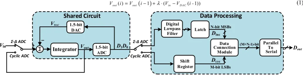
Fig. 2 shows the architecture of the presented two-stage hybrid ADC. The incremental Σ-Δ ADC, as the first stage, produces a serial digital bit stream and the residue voltage Vres. The bit stream is translated into N-bit MSBs by a digital lowpass filter. The
residue voltage is passed on to the second stage ADC (i.e. cyclic ADC) to obtain M-bit LSBs. The LSBs and MSBs are connected by the data connection module which costs 1-bit resolution to output the final (M+N-1)-bit digital signal. Σ-Δ ADC and cyclic ADC use the same integrator, 1.5-bit ADC and 1.5-bit DAC to perform conversion. Both stages adopt RSD algorithm to avoid the influence of comparator inaccuracy [9].
For the incremental Σ-Δ ADC, it takes 2N clock cycles for N-bit resolution. For each cycle, the input voltage
in
V is fed to the integrator in phase, and the feedback voltage VDAC( 1)i− is integrated in anti-phase at the same time. The output of integrator is
described as (1).
λ
is the gain of integrator in the incremental Σ-Δ ADC, andi
represents the number of clock cycles.( )
( ) 1 ( ( 1))
out out in DAC
V i =V i− + ⋅λ V −V i - (1)
Data Processing
Integrator 1.5-bitADC _
+ Vin
1.5-bit DAC
Data Connection Digital
Lowpass Filter
Σ-Δ ADC Σ-Δ ADC
Cyclic ADC Cyclic ADC
M-bit LSBs
Dinc
Dcyc N-bit MSBs
VDAC
Vout
Σ Module
Shared Circuit
Shift Register
Latch
Parallel To
Serial Dout
(M+N-1)-bit
D1D0
Fig. 2. Architecture of two-stage hybrid ADC
After 2N clock cycles, the Σ-Δ ADC exports the bit stream (2N bits) which can be transferred to N-bit digital data. The output voltage of integrator (2 )N
out
V is the residue voltage Vres.
Cyclic ADC has high conversion speed for it needs only M clock cycles for M-bit resolution. In the first cycle, the residue voltage
res
V (i.e. (2 )N out
V ) is quantized by the 1.5-bit ADC. During the rest cycles, the output voltage Vout(i−1) is fed to the integrator in phase and the feedback voltage VDAC( 1)i− is integrated in anti-phase to get Vout( )i , as shown in (2). The gain of integrator is changed
to 1 in the cyclic ADC. Vout( )i is evaluated by the 1.5-bit ADC to get other digital data.
( ) ( 1) ( ( 1) ( 1))
out out out DAC
V i =V i− + V i− −V i - (2)
B. Principle of Data Processing
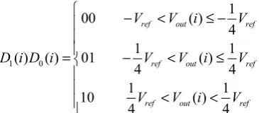
1 0
1
00 ( )
4
1 1
( ) ( ) 01 ( )
4 4
1 1
10 ( )
4 4
ref out ref
ref out ref
ref out ref
V V i V
D i D i V V i V
V V i V
− < ≤ −
= − < ≤
< <
(3)
The voltage VDAC( )i is exported from the 1.5-bit DAC which is controlled by D i D i1( ) 0( ), as shown in (4).
1 0
1 0
1 0 ( ) ( ) 00
( ) 0 ( ) ( ) = 01
( ) ( ) = 10
ref
DAC
ref
V D i D i
V i D i D i
V D i D i
− = = (4)
After 2N clock cycles, use N00, N01 and N10 to represent the number of
1( ) 0( )
D i D i which is 00, 01 and 10, respectively. The total sum of N00, N01 and N10 is 2N. We can get the residue voltage
res
V , as shown in (5).
10 00
10 01
[2 ( ) ]
1
[2 ( ) ( ) 2 ]
2
N
res in ref
N
in ref ref
V V N N V
V V N N V
λ
λ
= ⋅ ⋅ − − ⋅
= ⋅ ⋅ + − + ⋅ (5)
10 01
1 2
N + N is the N-bit output data of Σ-Δ ADC, regarded as Din c. Suppose Dc yc is the M-bit output data of cyclic ADC. Ignoring the quantization error of the cyclic ADC, we have
2 2
cyc
res ref M ref
D
V = V ⋅ −V (6)
According to (5) and (6), we can obtain
1
1
( 2 ) 2
2 2
M M
cyc inc
in M N ref ref
D D
V λ V V
−
+
− + ⋅
= ⋅ − (7)
In our design, the value of
λ
is 0.5. Equation (7) can be simplified as1 1
1 2
[( 2 ) 2 ]
2
ref
M M
in cyc inc M N ref
V
V D − − D V
+ −
= − + ⋅ ⋅ − (8)
We can see from (8) that the LSB of the two-stage hybrid ADC is 2 1 2
ref M N
V
+ − and M+N-1 bits resolution can be realized.
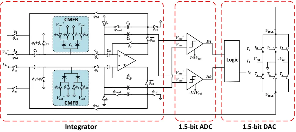
III. CIRCUIT DESIGN A. Implementation
The implementation of this hybrid incremental Σ-Δ/cyclic ADC is shown in Fig. 3. The integrator is of switched-capacitor type and it is symmetrical between the upper part and the lower part. The capacitor CH is used to eliminate the input offset voltage of
ϕ1d
D1
+
-+
ϕ1+ϕ3
ϕ2d
ϕ2
ϕ1+ϕ3
ϕ2
ϕ1d
ϕ3d
ϕ3d
ϕr
ϕr
ϕrd
ϕr
ϕrd
ϕrd
ϕrd
ϕ2d
S4
S2
S1
S3
Vin+
Vin
-ϕmod
ϕmod
C1 CH
C3
C2
D0
-1/4Vref
1/4Vref
Vout+
Vout+
Vout
-Vout
-Logic Vref
VDAC+
VDAC
-Integrator
1.5-bit ADC
1.5-bit DAC
-Vref
` C `
4
ϕ1 ϕ1 ϕ2d
Vout+ Vout
-ϕr
ϕ2d
` `
ϕ1 ϕ1 ϕ2d
Vout+ Vout
-ϕ2d CMFB
CMFB
T0
T1
T2
T0 T1
T2 T1
T2
T0
Fig. 3. Implementation of the hybrid incremental Σ-Δ/cyclic ADC
ϕ
rϕ
mode……
Reset
Mode Sigma-deltaIncremental Mode
Cyclic Mode
ϕ
1ϕ
2ϕ
3…… ……
……
2 cycles 256 cycles 7 cycles
Fig. 4. Time sequence of control signals
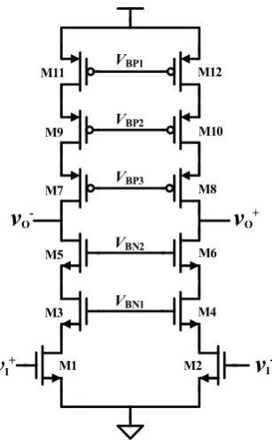
B. Pseudo-Differential OTA
VBN1 VBN2 VBP1
VBP2
VBP3
M1 M2
M3 M4
M5 M6
M7 M8
M9 M10
M11 M12
v
I+v
I-v
O-v
O+Fig. 5. Pseudo-differential OTA
C. CMFB Module
For high accuracy switched-capacitor circuit, the influence of charge injection cannot be ignored. Although charge injection can be suppressed by optimizing the aspect ratio of switch transistors and dummy transistors partly, there is still some charge (ΔQ), which can’t be eliminated in each clock cycle.It will cause serious drift of integrator’s common-mode output voltage with the accumulation of injection charge in 263 clock cycles.
Though pseudo-differential OTA itself needs no CMFB circuit, we add CMFB module to the integrator to suppress the influence of charge injection [11], as shown in Fig. 3. The capacitor CM is discharged to common-mood ground VC M at φ1 and forms a common-mode voltage detector at φ2. The difference between the common-mode voltage and VC M is fed to the integrator, realizing
a CMFB loop whose gain is defined as the ratio of CM / (C2+C3) in sigma-delta mood or CM/C2 in cyclic mood.
Suppose Vout( )n
+ and
( )
out
V− n is the output voltage of integrator at n-th clock cycle, ( )
cm
V n is the common-mode error of output voltage at n-th clock cycle, and VDAC( )n
+ and
( )
DAC
V− n is the output voltage of 1.5-bit DAC at n-th clock cycle.
During the incremental sigma-delta mode, the injection charge ΔQ causes integrator’s output voltage shift
Δ
v
in every clock cycle, andΔ
v
is equal to ΔQ/ (C2 +C3). We have (9) and (10) shown as follow.2 3
( 1)
( 1) ( ) ( ( )) cm M
out out in DAC
V n C
V n V n V V n v
C C
λ
+ + = + + ⋅ +− + − + ⋅ + Δ
+ (9)
2 3
( 1)
( 1) ( ) ( ( )) cm M
out out in DAC
V n C
V n V n V V n v
C C
λ
− + = − + ⋅ −− − − + ⋅ + Δ
+ (10) Adding (9) and (10), we can acquire (11).
2 3
( 1)
( 1) ( ) cm M
cm cm
V n C
V n V n v
C C
+ ⋅
+ = − + Δ
+ (11) Equation (11) can be obtained by iteration method.
2 3 2 3 2 3
2 3 2 3
( ) ( )n (0) (1 ( ) )n
cm cm
M M M
C C C C C C
V n V v
C C C C C C C
+ + +
= ⋅ + ⋅ − Δ
+ + + + (12)
2 3
(256)
cm
M M
C C Q
V v
C C
+ Δ
≈ ⋅ Δ = (13)
There are 7 clock cycles in cyclic mode, and the variation Δy caused by charge injection is ΔQ C/ 2 in each clock cycle. We have
(14) and (15) shown as follow.
2
( 1)
( 1) ( ) ( ( ) ( )) cm M
out out out DAC
V n C
V n V n V n V n y
C
+ + = + + + − + − + ⋅ + Δ (14)
2
( 1)
( 1) ( ) ( ( ) ( )) cm M
out out out DAC
V n C
V n V n V n V n y
C
− + = − + − − − − + ⋅ + Δ (15)
Adding (14) and (15), we can acquire (16) and (17).
2
( 1)
( 1) 2 ( ) cm M
cm cm
V n C
V n V n
C y
+ ⋅
+ = − + Δ (16)
2 2
2 2
2 2
( 1) ( )
2
cm cm
M M
C C y
V n V n
C C C C
Δ
+ = ⋅ + ⋅
+ + (17) Suppose Vcm(final) is the final common-mode error of output voltage.
7 7
2 2 2
2 2 2
7 7
2 2
2 2 2
2 2
(final) ( ) (256) (( ) 1)
2 2
( ) (( ) 1)
cm cm
M M M
M M M M
C C C
V V y
C C C C C C
C Q C Q
C C C C C C C
= ⋅ + − ⋅ ⋅ Δ + + − Δ Δ ≈ ⋅ + − ⋅ + + − (18)
The value of CM should be much smaller than C2 for the limitation of system bandwidth, so (18) can be simplified as (19).
7 2
2 2
2 1 1
(final) ( ) ( )
cm
M M M
C
V Q
C C C C C
≈ ⋅ + ⋅Δ
+ − (19)
Take a derivative with respect to (19), we learn Vcm(final) is decreased with the increase of CM in the interval of
2
1 2
[0, ]
3 C
+ . Considering the limitation of system bandwidth, we adopt
2/ 6 M
C =C , which limits the value of Vcm(final) to
(
2)
313⋅ ΔQ C/ . By contrast, the value of Vcm(final) will be greater than 16384⋅ Δ
(
Q C/ 2)
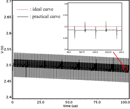
without the CMFB module. It is can also beverified by simulation. We take the common-mood ground VC M (i.e. 2.5 V) as each single-ended input signal, and the output level
of integrator is the common-mode output voltage. Without the CMFB module, the final common-mode output voltage of integrator drifts obviously after 256 cycles, as shown in Fig. 6. By contrast, the final common-mode output error Vcm(final) is well suppressed by the CMFB module, as shown in Fig. 7. The hybrid ADC will be out of work in the cyclic mode without the CMFB module.
: ideal curve : practical curve
: ideal curve : practical curve
Fig. 7. Simulation result with CMFB module
IV. EXPERIMENTAL RESULTS
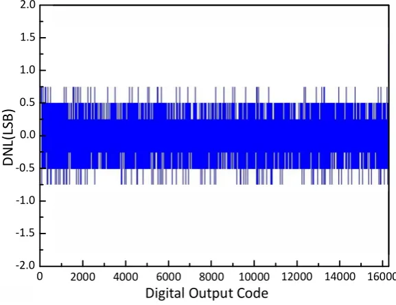
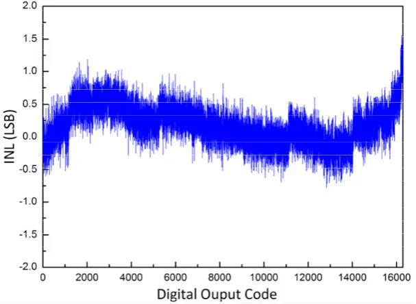
A test chip of the hybrid ADC is fabricated in 0.35μm 2P4M CMOS technology. The digital circuit used to generate control signals can be shared by all channels. The area of the analog circuit is 0.094 mm2. As power supply of the front-end circuit in ROIC is 5V, the analog circuit in this ADC is supplied with 5V and the digital part is supplied with 3.3V. The single-ended input voltage range is 1.2V~3.8V. The ADC works at a clock frequency of 2.5MHz.
The static and dynamic performance is measured by Ultra Flex1600 with 16-bit DAC for input voltage generation. A quasi-DC voltage ramp is used as input for static measurement. The plot of DNL is shown in Fig. 8 with the root mean square (RMS) value of 0.254 LSB. The plot of INL is shown in Fig. 9 with the maximum value of -0.776/+1.56 LSB. An 800Hz sinusoidal signal is used as the input signal to perform the dynamic test. The amplitude of sinusoidal signal is 1.3V~3.7V, which is close to the full scale. Fig. 10 shows the power spectral density of the output data. The spectrum shows the pseudo-differential structure with CMFB module suppresses the even harmonic effectively. The measured ENOB achieves 13.43-bit, which is close to the theoretical resolution of 14-bit. The test results of the chip are listed in Table I.
0.0
-0.5
-1.0
-1.5
-2.0 0.5 1.0 1.5 2.0
DN
L(L
SB)
0 2000 4000 6000 8000 10000 12000 14000 16000
Digital Output Code
Fig. 9. Plot of INL
Frequency [Hz]
Po
w
e
r Sp
ect
ra
l D
e
n
si
ty
[d
B]
Fig. 10.Power spectral density of output data
TABLE I. TEST RESULTS
performance Test results
DNL (RMS) 0.254 LSB
INL (MAX) -0.776/+1.56 LSB
SFDR 94.55dB
THD 93.86dB
ENOB 13.43-bit
V. CONCLUSION
REFERENCES
[1] W. Rieutort-Louis, T. Moy, Z. Wang, et al. “A large-area image sensing and detection system based on embedded thin-film classifiers,” Solid-State Circuits, IEEE Journal of, 2015, vol.pp(99), pp:1-10.
[2] Y. Yao, H. Bornefalk, S.S. Hsieh, M. Danielsson, J.N. Norbert, “Utilization of in-depth photon counting detectors towards x-ray spectral imaging: The benefits from the depth information,” Biomedical Imaging (ISBI), 2014 IEEE 11th International Symposium on. IEEE, 2014, pp.1156-1159.
[3] Chu C, Bruckner T, Kauffman J G, et al. Analysis and design of high speed/high linearity continuous time delta-sigma modulator[C]//Circuits and Systems (ISCAS), 2013 IEEE International Symposium on. IEEE, 2013: 1268-1271.
[4] S. Yeh, C. Hsieh, “Novel Single-Slope ADC Design for Full Well Capacity Expansion of CMOS Image Sensor,” IEEE Sensors Journal, 2013, vol.13(3), pp:1012-1017.
[5] Chae Y, Cheon J, Lim S, et al. A 2.1 M pixels, 120 frame/s CMOS image sensor with column-parallel ADC architecture[J]. Solid-State Circuits, IEEE Journal of, 2011, 46(1): 236-247.
[6] S. Lim, J. Cheon, Y. Chae, et al. “A 240-frames/s 2.1-Mpixel CMOS image sensor with column-shared cyclic ADCs,” Solid-State Circuits, IEEE Journal of, 2011, vol.46(9), pp:2073-2083.
[7] Gao L, Ding R, Zhou J, et al. A low-power SAR ADC for IRFPA ROIC[C]//Photonics Asia. International Society for Optics and Photonics, 2012: 856210-856210-8.
[8] L. Rossi, S. Tanner, P.A. Farine, “Performance analysis of a hybrid incremental and cyclic A/D conversion principle,” Circuits and Systems I: Regular Papers, IEEE Transactions on, 2009, vol.56(7), pp:1383-1390.
[9] G.N. Angotzi, M. Barbaro, P.G.N. Jespers, “Modeling, evaluation, and comparison of CRZ and RSD redundant architectures for two-step A/D converters,” Circuits and Systems I: Regular Papers, IEEE Transactions on, 2008, vol.55(9), pp:2445-2458.
[10] A.N. Mohieldin, E. Sánchez-Sinencio, J. Silva-Martínez, “A fully balanced pseudo-differential OTA with mode feedforward and inherent common-mode feedback detector,” Solid-State Circuits, IEEE Journal of, 2003, vol.38(4), pp:663-668.
[11] Y. Chae, G. Han, “Low voltage, low power, inverter-based switched-capacitor delta-sigma modulator,” Solid-State Circuits, IEEE Journal of, 2009, vol.44(2), pp:458-472.