1
International Journal in Physical and Applied Sciences http://ijmr.net.in, Email: [email protected]Effect of Cobalt doping on the structural and optical properties of TiO
2thin films prepared by sol-gel technique.
Davinder Singha , Alka Goyal b , Neenu Sainic
*
a
Pt.JLN Govt. College Faridabad, 121002, India.
b
D.A.V. College for Girls, Yamuna Nagar 135001, India
c
Pt.JLN Govt. College Faridabad, 121002, India.
Abstract
In this study, Pure and Co doped titanium dioxide (TiO2) thin films on glass substrate were prepared by using sol-gel dip coating process. The effects of Co doping on the structural and optical properties of TiO2 thin films were investigated. The as-prepared films were annealed at temperature 500C for 1h and characterized by X-ray diffraction (XRD), atomic force microscopy (AFM) and UV-Visible spectroscopic studies. The XRD patterns and AFM images revealed a polycrystalline structure for all samples. Optical band gap, refractive index, optical conductivity and extinction coefficients of these films were determined using transmittance spectra. Band gap energy of the Co doped anatase TiO2 films is found to decrease with increasing Coconcentration. The refractive index was found to increase from 2.12 to 2.33 with increase in Co concentration from 0 to 1.0-mol %.
Keywords: Co-doped TiO2; Sol Gel; Thin Films; Optical band gap;
1.
Introduction
2
International Journal in Physical and Applied Sciences http://ijmr.net.in, Email: [email protected]2. Experimental
2.1. Preparation of TiO2 precursor sol
A 0.5M TiO2 solution was prepared by the partial hydrolysis and poly-condensation of titanium tetra-butoxide with water using isopropyl alcohol (IPA) as a solvent and HNO3 as a catalyst reported earlier [8 S. D sharma , 2006]. All the chemicals used were of AnalaR grade and were used as procured i.e. without further purification. The solution was kept overnight before film deposition.
2.2. Preparation of pure TiO2 and Co/TiO2 thin films
For the film deposition, the substrates were ultra cleaned thoroughly and dried before deposition. Then the substrate was dipped in the precursor solution bath and pulled out with a constant speed of 24 cm/min to obtain the films of uniform thickness. A very thin film of TiO2 that formed on the substrate was first dried in air at room temperature, followed by drying at 100C for 30 min in an electric oven. The films formed were further heated at 500 C for 1 h in an electric furnace. For the preparation of the cobalt doped titania films, the procedure was performed as described above; besides that, the appropriate amount of cobalt acetylacetonate [Co (acac) 2] from 0.1 to 1.5 mol % was dissolved in the TiO2 precursor sol.
2.3. Characterization techniques
AFM and XRD studies were performed to get the structure and final phase formation.
XRD spectra of the samples have been recorded in the 2
ranges 20
to 80
for crystal
phase identification with a SIEMENS D-500 diffractometer using monochromatized
CuK
radiation (
= 1.541Å). The nanoparticle size and surface morphology were studied
using a Nanoscope IIIa Atomic Force Microscope (AFM). Transmission and absorption
spectra were recorded from 300 nm – 800 nm with a SHIMADZU UV-3101 PC UV-VIS
spectrophotometer at normal incidence
.
3. Results and discussion
3.1. XRDXRD patterns of pure, 0.5 and 1.5-mol% cobalt doped TiO2 thin films calcined at 500C are shown in the Fig. 1. Only anatase phase was identified for pure and doped TiO2 films. The average grain size of the particles is calculated from peak broadening by Scherer equation.
Cos
0.94
L
[9 B.D. Cullity,1978]3
International Journal in Physical and Applied Sciences http://ijmr.net.in, Email: [email protected] Fig. 1 XRD spectra of (a) undoped TiO2 and (b) 1.5 mol% Co doped TiO2 thin films3.2. AFM Observation.
4
International Journal in Physical and Applied Sciences http://ijmr.net.in, Email: [email protected]100 nm
50 nm
0 nm
100 nm
50 nm
0 nm
99.95 nm 49.97 nm 0 nm
100 µm
50 µm
0 µm
100 µm
50 µm
0 µm
200 nm 100 nm 0 nm
100 µm
50 µm
0 µm
100 µm
50 µm
0 µm
100 nm 50 nm 0 nm
(b)
(a)
(c)
5
International Journal in Physical and Applied Sciences http://ijmr.net.in, Email: [email protected] 3.2 Photoluminescence of Co doped TiO2 films.400 450 500 550 600 650
0 5000 10000 15000 20000 25000 30000 35000 40000 45000 50000 55000 60000 65000 70000 75000
In
te
n
si
ty
Energy (eV)
Pure TiO
2 film
0.5 mol% Co/TiO2 film 1.5 mol% Co/TiO2 film
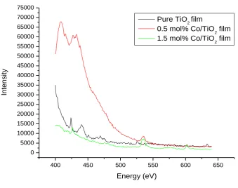
Fig. 3. Photoluminescence of pure, 0.5 and 1.5 mol% Co doped TiO2
Fig 3. Shows the PL of Co doped TiO2 films excited at 335 nm in the region from 400 nm to 650 nm. As it is clear from the figure that there is blue shift due to increase in Co concentration. The PL intensity decreases with increase in dopant concentration up to 1.0 mol%. There are four peaks corresponding to transitions from 4D 7/2→
4 F 3/2,
4 D 7/2→
4 F 5/2,
4 D 7/2→
4
F 7/2 and 4
D 7/2→ 4
F 9/2.
3.3. Transmittance
6
International Journal in Physical and Applied Sciences http://ijmr.net.in, Email: [email protected]300 400 500 600 700 800
0.0 0.2 0.4 0.6 0.8 1.0
T%
Wavelength (nm) Pure TiO2 film
0.5 mol% Co/TiO2 film
1.5 mol% Co/TiO2 film
Fig. 4. Transmittance spectra of Pure and Co doped TiO2 films.
The fast decrease in the transmittance below 400 nm is due to absorption of light caused by excitation of electrons from valence band to conduction band of TiO2 [12 M. M. Rahman,1999]. Band edge absorption shifts towards the longer wavelength side, which shows the red shift and indicating the decrease in band gap.
3.4. Optical band gap
Determination of band gap energy (Eg) is often necessary to develop the electronic band structure of thin materials. In high absorption region (>104/cm) absorption coefficient is related to the incident photons energy h by this relation, which is known as Tauc's equation [13 X. K. Zhao].
h
E
E
B
p g
Where B is a constant and p is an index that characterizes the optical absorption process and is theoretically equal to1/2, 2, 3/2 or 3 for direct allowed, indirect allowed, direct forbidden and indirect forbidden transitions, respectively. Best fit in optical absorption data obtained from many oxide films as achieved when p=2, [14. I. B. Lucy, 1995]
The absorption coefficient () of undoped and Co doped samples was calculated from the transmittance by using the following formula
T Log d
1 1
[15 D. Mardare, 2000].Where d is the thickness of the film and T is the transmittance.
7
International Journal in Physical and Applied Sciences http://ijmr.net.in, Email: [email protected] 0.5, and 1.5 Mol % Co doped TiO2 samples respectively. The decrease in the band gaps of Co doped TiO2 may be due to the introduction of electronic states by impurity Co 3d electrons.2.0 2.1 2.2 2.3 2.4 2.5 2.6 2.7 2.8 2.9 3.0 3.1 3.2 3.3 3.4 3.5 3.6 3.7 3.8 3.9 4.0 0
2000 4000 6000 8000 10000 12000
(
h
)
1
/2
Energy (eV) Pure TiO
2 film
0.5 mol% Co/TiO
2 film
1.5 mol% Co/TiO
2 film
Fig. 5. Optical band gaps of Pure and Co doped TiO2 films.
3.5. Refractive index
Refractive index, n () of the pure TiO2 and Co doped TiO2 films corresponding to wavelength at first order transmittance minima position has been determinedfromabsolute Tmin value provided no and n2 are known by using the following formula [16 Manoj Sreemany,2004]
min min 2
0
1
1
T
T
n
n
n
n =1 (refractive index of air) and n2=1.515 (refractive index of soda glass).
8
International Journal in Physical and Applied Sciences http://ijmr.net.in, Email: [email protected]
1
2
2
1
2 2 2 2 b b f f b fn
n
n
n
P
[20 C.R. Ottermann, 1996]
Where nf and nb are the refractive indices of the film and the bulk material of TiO2. The
Ρf and Ρb are the density of the film and bulk material respectively.
0.0 0.2 0.4 0.6 0.8 1.0 1.2 1.4 1.6
0.0 0.2 0.4 0.6 0.8 Pa ck in g d e n si ty
Conc. of Co
B
Fig. 6. Packing density of Co/TiO2 films
The packing density of the films was calculated from refractive index values.
Porosity was calculated by using the following formula
1
1
1
2 0 2n
n
Porosity
[21 B. E. Yoldas, 1985]Where n0 is the refractive index of the pore free antase (n0=2.52) [22W. D.Kingery, 1976] and n is the refractive index of the porous thin film. Porosity of these films lies in the range from to 34.68 %. to 17.22 for n=2.12 and n=2.33. The decrease in porosity by cobalt doping indicates the densification of TiO2 thin films. The same is supported by AFM analysis.
3.6. Extinction Coefficient
Fig. 7. Shows the variation of extinction coefficient k () with wavelength of undoped and Co doped TiO2 thin films in the range of wavelength 300 to 800 nm. Extinction coefficient increases with increase amount of Cobalt in pure TiO2. It is calculated by using the formula
4k 400 500 600 700 800
0.00 0.05 0.10 0.15 0.20 0.25 0.30 0.35 0.40 0.45 Ext inct ion co eff icien t Wavelength (nm) Pure TiO2 film 0.5 mol% Co/TiO2 film 1.5 mol% Co/TiO2 film
d e m o d e m o d e m o d e m o
d e m o d e m o d e m o d e m o
d e m o d e m o d e m o d e m o
d e m o d e m o d e m o d e m o
d e m o d e m o d e m o d e m o
d e m o d e m o d e m o d e m o
d e m o d e m o d e m o d e m o
d e m o d e m o d e m o d e m o
d e m o d e m o d e m o d e m o
9
International Journal in Physical and Applied Sciences http://ijmr.net.in, Email: [email protected] The AFM results show that the surface of sample 1.5 mol% Co doped TiO2 is rougher than the other Co doped samples. So if the light scattering is due to the surface roughness, then 1.5 mol % Co doped TiO2 film should have higher extinction coefficient. Similar effect of surface roughness on the extinction coefficient is reported [23 Li-Jian Meng, 2006].3.7. Optical conductivity
From the absorption coefficient we have calculated the optical conductivity opt as
4 nc
opt [24. J. I. Pankove, 1975]
Where is the absorption coefficient, n is refractive index and c is the velocity of light. Fig. 8. shows the variation of optical conductivity as function of photon energy h. For positive or negative inhomogeneous films the maximum transmittance will increase or decrease a little, which will sssssssssssssscause errors in the refractive index and optical conductivity. Optical conductivity of pure and cobalt doped TiO2 thin films is in the range of 10
14
to 1015 sec-1.
1.5 2.0 2.5 3.0 3.5 4.0
-1.00E+014 0.00E+000 1.00E+014 2.00E+014 3.00E+014 4.00E+014 5.00E+014 6.00E+014 7.00E+014 8.00E+014 9.00E+014
O
pt
ical
C
on
du
ct
iv
ity
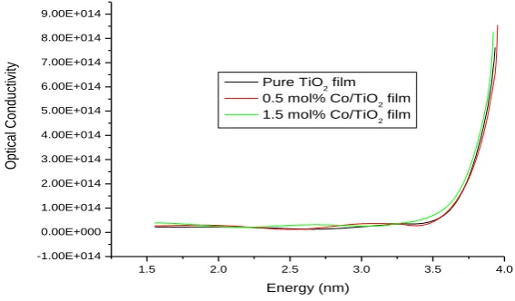
Energy (nm) Pure TiO2 film 0.5 mol% Co/TiO2 film 1.5 mol% Co/TiO2 film
Fig. 8. Variation of Optical Conductivity Vs Photon Energy.
The increase in optical conductivity at high photon energies is due to high absorbance of the TiO2 thin films and may also be due to electron excited by photon energy. [25 F. Yakuphanoglu, 2005]
4. Conclusions
10
International Journal in Physical and Applied Sciences http://ijmr.net.in, Email: [email protected]5.Acknowledgements
Authors are highly thankful to director National Physical Laboratory New Delhi for providing laboratory facilities We are also thankful to Dr. Nefa Singh, Dr. K.K. saini for their help in this work.
References
1. D. Mergela, U.D. Buschendrorfa, S. Eggerta, R. Grammesb, B. Samsetc, Thin Solid Films, 371, (2000), 218.
2. S. A. Chamber, S. Thevuthasan, R. F. C. Farrow, R. F. Marks, J. U. Thiele, L.Folks 3. N. J. Seong, S. G. Yoon, C.R. Cho, Appl. Phys. Lett. 81, (2002), 4209.
4. N. H. Hong, J. Sakai, W. Prellier, A. Hassini, Appl. Phys. Lett. 83, (2003), 3129. 5. E. Haro-Poniatowski, S. V. Munos, a. Murillo, Mater. Res. Bulletin, 31, (1994), 329. 6. J. R. Simpson, H. D. Drew, S. R. Shinde, R. J. Choudhary, S. B. Ogale, T.
Venkatesan, Phys. Rev. B 69, (2004), 193205.
7. P. Chrysicopoulou, D. Davazoglou, Chr. Trapalis, G. Kordas, Thin Solid, 323,
8. S. D. Sharama, Davinder Singh, K. K Saini, C. Kant, V. Sharama, S. C. Jain, C.P. Applied Catalysis A; Gen., 314, (2006), 40.
9. B.D. Cullity, Elements of X-ray Diffraction, Addison-Wesley, Notre Dame, 1978.
10. Y. Leprince Wang, K.Yu Zhang, Surface and Coating Technology 140, (2001) 155.
11. Radha devi chekuri, Shiva Rao Trikkovalluri, South African journal of chemical Engineering, 24(2017)183/195
12. M. M. Rahman, K. M. Krishan, T. Soga, T. Jimbo, M. Umeno Journal of Phys and Chem of Solids 60, (1999), 201.
13. X. K. Zhao, J. H. Fendler, Phys. Chem. 95, (1991), 3716.
14. I. B. Lucy, J. Benynon, D. N. Waters, Mater Sci. Letters, 14, (1995), 515.
15. D. Mardare, M.Tasca, M. Delibas, G. I. Rusu, Applied Surface Science156, (2000), 200. 16. Manoj Sreemany, Suchitra Sen, materials Chemistry and Physics 83, (2004}, 69.
17. L. Hu, T. Yoko, H. Kozuka, S. Sakka, Thin Solid films, 219, (1992), 18. 18. C. Kittle, Solid State physics, John Willey& Sons, New York, 1971.
19. W. Heitman, Thin Solid Films, 5, (1970), 61.
20. C.R. Ottermann, K. Bange, Thin Solid Films 286, (1996), 32. 21. B. E. Yoldas, P. W. Partlow, Thin Solid Films, 129, (1985), 1.
22. W. D. Kingery, H. K. Bowen, D. R. Uhlmann, Introduction to Ceramics, Wiley, NY, 1976.
23.
Li-Jian Meng, V. Teixeira, H.N. Cui, Frank Placido, Z. Xu, M.P. dos
24.
Santos,Applied Surface Science 252, (2006), 7970.
25.
J. I. Pankove, Optical processes in semiconductor, Dove Publications Iac, New
York, 1975, p 91.