Available Online at www.ijcsmc.com
International Journal of Computer Science and Mobile Computing
A Monthly Journal of Computer Science and Information Technology
ISSN 2320–088X
IJCSMC, Vol. 4, Issue. 7, July 2015, pg.388 – 395
RESEARCH ARTICLE
An Improved Implementation of 4-bit
Multiplier Using Reversible Gates
Karanjot Kaur
M.Tech Student (ECE), Rayat & Bahra Institute of Engg. and Technology, Kharar, Punjab, India
Abstract— Reversible circuits, their optimization and synthesis is a major emerging field in research now-a-days. Various researchers have contributed much in this area so far. Reversible logic has received great attention in the recent years due to their ability to reduce the power dissipation which is the main requirement in low power VLSI design. Quantum computers are constructed using reversible logic circuits. It has wide applications in low power CMOS and Optical information processing, DNA computing, quantum computation and nanotechnology. In this paper, a 4-bit reversible multiplier is proposed with lower quantum cost w.r.t existing reversible multiplier circuits. Reversible circuits have a great advantage over irreversible ones that very less energy is dissipated and there is one-to-one mapping between the inputs and outputs. It is hoped that this provides a little milestone in this field of research.
Keywords— Reversible Logic, Quantum Cost, Constant inputs, Garbage Outputs, Reversible Multiplier, Nanotechnology
I. INTRODUCTION
Conventional combinational logic circuits dissipate heat for every bit of information that is lost during their operation. Due to this fact the information once lost cannot be recovered in any way. But the same circuit, if it is constructed using the reversible logic gates will allow the recovery of the information. In 1960s R. Landauer demonstrated that even with high technology circuits and systems constructed using irreversible hardware, results in energy dissipation due to information loss [1].He showed that the loss of one bit of information dissipates KTln2 joules of energy where K is the Boltzman‟s constant and T is the absolute temperature at which the operation is performed [1]. Later Bennett, in 1973, showed that this KTln2 joule of energy dissipation in a circuit can be avoided if it is constructed using reversible logic circuits [2]. The gate/circuit that does not loose information is termed as reversible logic or the reversibility. A reversible circuit has the facility to generate a unique output vector from each input vector and vice versa.
Reversible Logic or Reversibility is defined as that gate or circuit that does not loose information. A Reversible
circuit has the facility to generate a unique Output vector from each input vector and vice versa.
Input Vector: Iv= Iij, Ii+1j,Ii+2j,……Ik-1j,Ikj
Output Vector: Ov=Oij, Oi+1j, Oi+2j…..Ok-1j,Okj
For each Particular vector j
Reversible are circuits in which the number of inputs is equal to the number of outputs and there is one to one
mapping between vectors of inputs and outputs. A Gate with „k‟ inputs and „k‟ Outputs is called k*k gate
.
i
1o
1i
2o
2i
3o
3i
k-1o
k-1i
ko
kFig. 1 Reversible Circuit Block Diagram
From the point of view of reversible circuit design, there are many parameters for determining the complexity and
performance of circuits.
The number of Reversible gates (N): The number of reversible gates used in circuit.
The number of constant inputs (CI): This refers to the number of inputs that are to be maintained
constant at either 0 or 1 in order to synthesize the given logical function.
The number of garbage outputs (GO): This refers to the number of unused outputs present in a reversible
logic circuit. One cannot avoid the garbage outputs as these are very essential to achieve reversibility.
Quantum cost (QC): This refers to the cost of the circuit in terms of the cost of a primitive gate. It is
calculated knowing the number of primitive reversible logic gates (1*1 or 2*2) required to realize the
circuit.
Gate levels (GL): This refers to the number of levels in the circuit which are required to realize the given
logic Functions.
The main rules for efficient reversible Logic Synthesis are as follows:-
Use as many outputs of every gate as possible and thus minimize the garbage outputs.
Do not create more constant inputs to gates that are absolutely necessary.
Avoid leading output signals of gates to more than one input i.e. Fanout is banished.
Don‟t use feedback loop as it is strictly prohibited.
Use as less number of Reversible Gates as possible to achieve the goal.
II. OVERVIEW OF BASIC REVERSIBLE GATES
The simplest reversible gate is NOT Gate and is a 1*1 gate. Controlled Not (CNOT) gate is an example for a
2*2 gate. There are many 3*3 reversible Gates such as Fredkin (F), Toffoli(TG) and Peres(PG) gate. The
Quantum cost of a 1*1 gate is zero and Quantum cost of a 2*2 gate is one. Any reversible gate is realised by
using 1*1 NOT gates and 2*2 reversible gates such as V, V+ (V is Square Root of NOT Gate and V+ is its
hermitian) . Feymann Gate is also known as CNOT Gate. The V and V+ quantum gates have the properties
given in following equations:-
V*V=NOT
V* V+= V+* V=I
V+* V+=NOT
A. NOT Gate
The Logic NOT Gate is used as a reversible gate as it has one input and an corresponding output. It is a single
input device which has an output level that is normally at logic level “1” and goes “LOW” to a logic level “0” when its single input is at logic level “1”, in other words it “inverts” (complements) its input signal. The output
from a NOT gate only returns “HIGH” again when its input is at logic level “0” giving us the Boolean
expression of: A = A‟.
A
A‟
Fig 2. 1*1 Reversible NOT gate
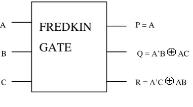
B. FREDKIN GATE
Just as there can be universal gates for classical irreversible computing, such as the NAND gate (which has two
inputs and one output), so too can there be universal gates for classical reversible computing. However, the
smallest gates that are both reversible and universal require three inputs and three outputs. Two well-known
examples are the FREDKIN (controlled-SWAP) gate and the TOFFOLI (controlled CNOT) gate
.
A P = A
B Q = A‟B AC
C R = A‟C AB
Fig 3. 3*3 Fredkin gate
C. Feyman Gate
The basic 2*2 Feyman gate (FG) is shown in Figure4 [3]. It has two input bits A & B and corresponding two
output bits as P & Q. From its logic computation table given as table, it can be observed that the Feyman gate is
reversible. In addition to its reversibility, it does not exhibit parity preserving logic which is widely adapted for
fault detection in communication systems.
A
P = A
B
Q = A
B
Fig 4. 2*2 Feynman gate
D.TOFFOLI GATE
The basic 3*3 Toffoli gate (TG) is shown in Figure5 [4]. It has three input bits A, B & C and corresponding
three output bits as P, Q & R. From its logic computation table given in table IV, it can be observed that the
Toffoli gate is reversible. In addition to its reversibility, it does not exhibit parity preserving logic.
FREDKIN
GATE
FG
Reversible
A
P = A
B
Q = B
C
R = AB C
Fig 5. 3*3 Toffoli Gate
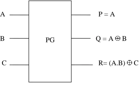
E. PERES GATE
The basic 3*3 Peres gate (PG) is shown in Figure6 [5]. It has three input bits A, B & C and corresponding three
output bits as P, Q & R. From its logic computation table it can be observed that the Peres gate is reversible.
A
P = A
B
Q = A B
C
R= (A.B) C
Fig 6. 3*3 Peres Gate
III. PREVIOUS WORK
So far, large work has been done in order to implement reversible circuits. Multiplier is such a part of the circuit that fastens or slows down the processing power of a circuit. However, if we implement the multiplier circuit using reversible gates a lot of energy consumption will be reduced and efficiency of the circuit will be increased manifold. This section details about the implementation of reversible multiplier using reversible gates such as Toffoli gate which is effective in terms of number of reversible gates, number of garbage outputs, number of constant inputs, quantum cost and hardware complexity.
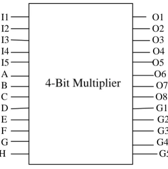
IMPLEMENTATION OF REVERSIBLE 4 BIT MULTIPLIER
The Proposed 4*4 Reversible Multiplier circuit has been designed and implemented using Toffoli gates only. This proposed Design is using only Toffoli gates because it is the universal gate of reversible logic which means any gate can be derived from Toffoli gate. This makes the design implementation easy and convenient to use.
In the 4 bit multiplier, 13 inputs and 13 outputs are used in which we have five constant inputs - I1, I2, I3, I4 ,I5 eight inputs- A, B, C, D, E, F, G, H, , eight outputs – O1, O2, O3, O4, O5, O6, O7, O8 and five garbage outputs – G1, G2, G3, G4,G5 as shown in Fig 5.
I1 O1 I2 O2 I3 O3 I4 O4 I5 O5 A O6 B O7 C O8 D G1 E G2 F G3 G G4 H G5
Fig 5. Reversible 4 bit Multiplier
IV. RESULTSANDDISCUSSION
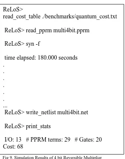
The implementation of design is done on Ubuntu 14.04 (LTS) / Relos tool which simulates and synthesizes the reversible logic circuit based on positive-polarity Reed-Muller expressions [9]. Simulation results of reversible 4 BIT Multiplier are shown as follows in Fig. 6.
Fig 7. PPRM Specification for 4-bit Reversible Multiplier
4-Bit Multiplier
# pprm for multi4bit
.model multi4bit
.inputs i1 i2 i3 i4 i5 a b c d e f g h
.z 1 1 1 1 1 0 0 0 0 0 0 0 0
.p 0000000000001 0000000000001
.p 0000000000010 0001000000010
.p 0000000000011 0001000000000
.p 0000000000100 0010000000100
.p 0000000000101 0010000000000
.p 0000000001000 0100000001000
.p 0000000001001 0100000000000
.p 0000000010000 1000000010000
.p 0000000010001 1000000000000
.p 0000000100000 0001000100000
.p 0000000100001 0001000000000
.p 0000000100010 0001000000000
.p 0000001000000 0010001000000
.p 0000001000001 0010000000000
.p 0000001000100 0010000000000
.p 0000010000000 0100010000000
.p 0000010000001 0100000000000
.p 0000010001000 0100000000000
.p 0000100000000 1000100000000
.p 0000100000001 1000000000000
.p 0000100010000 1000000000000
.end
Once the Positive Polarity Reed Muller (PPRM) Specifications are achieved and a best Solution is obtained, the next step is to create a Netlist.. A Netlist consists of a list of the terminals ("pins") of the electronic components in a circuit and a list of the electrical conductors that interconnect the terminals. The Netlist of the proposed Design is specified as follows in fig 8.
Fig 8. Netlist created by Relos
The Final step is to calculate the Quantum Cost, No. of gates used, Garbage Outputs and Constant inputs which
can be generated by using the commands as write_netlist, read_cost_table, print_stats.
# Netlist generated by command
'write_netlist' in ReLoS
.model multi4bit
Fig 6. Simulation Results of 4-bit Reversible Multiplier
Fig 9. Simulation Results of 4 bit Reversible Multiplier
Table I shows the reversible 4 Bit Multiplier comparison of proposed design with the previously designed Multiplier using different implementing methods and synthesis tools. Comparison is made in terms of number of real and constant inputs, number of gates used, and number of operations performed and the quantum cost of the circuit. In the designed Multiplier, number of real and constant inputs is lesser as compared to the previous 4 bit Multiplier.
Table I
Comparison of Existing and Proposed Multiplier Designs
Constant Inputs Garbage Outputs Gate Count Quantum Cost
Proposed 5 5 20 68
[8] 46 46 45 237
[6]Design1(HNG,PG,TG) 28 28 28 137
[6]Design 2(PG,TG) 28 28 36 153
[7] 40 40 32 140
[10] 28 52 28 Not Defined
[11] Not Defined 56 28 Not Defined
[12] 20 28 20 104
It is clearly evident from the above table that the proposed design is better and efficient in terms of Constant
Inputs, Garbage Outputs, Gate Count and most importantly Quantum cost.
V. CONCLUSION
Reversible 4 Bit Multiplier is successfully designed using Tofolli gates having lesser cost as compared to previous ones. The hardware complexity and power saving are decreased thereby reducing cost.
ReLoS>
read_cost_table ./benchmarks/quantum_cost.txt
ReLoS> read_pprm multi4bit.pprm
ReLoS> syn -f
time elapsed: 180.000 seconds
.
.
.
.
.
.
...
ReLoS> write_netlist multi4bit.net
ReLoS> print_stats
REFERENCES
[1] Landauer,R, “Irreversibility and Heat Generation in the Computational Process” IBM J. of research and Development Vol.5, pp. 183-191, 1961.
[2] Bennett, C.H, “Logical Reversibilty of Computation” IBM J. of research and Development Vol 17 pp. 525-532,1973.
[3] Feymann.R(1985) “Quantum Mechanical Computers” Optical News,Vol.11,pp.11-20.
[4] Toffoli,T.(1980) , “Reversible Computing” Technical Memo MIT/LCS/TM-151,MIT Laboratory for
Computer Sciecnce(February).
[5] Peres,A.(1985), “Reversible Logic and Quantum Computers”, Physical Reviews.A,32:1985,pp.3266-3276.
[6] Majid Haghparast (2009), “ An Optimized Reversible Multiplier Circuit,” Journal of circuit System and
Computers, Vol. 18,pp. 1-13.
[7] H.G Rangaraju, AAkash Babu Suresh and K.N Muralidhara(2013), “Design of Efficient Reversible Multiplier”, Springer Publications, Vol.3 pp. 571-579.
[8] Hatkar A.P, Hatkar A.A and Narkhede N.P (2014), “ASIC Design of Reversible Multiplier Circuit”, IEEE Transaction, Vol. 29, pp. 47-52.
[9]Gupta, P.; Agrawal, A. and Jha, N. K. (2006), “An Algorithm for Synthesis of Reversible Logic Circuits,” IEEE Trans. CAD, vol. 25, 11, pp. 2317–2330.
[10] Majid Haghparast, Somayyeh Jafarali Jassbi, Keivan Navi and Omid Hashemipour (2008), “Design of a Novel Reversible Multiplier Circuit Using HNG Gate in Nanotechnology”, World Applied Sciences Journal, Vol 3, pp.974-978.
[11] Masoumeh Shams, Majid Haghparast and Keivan Navi(2008), “Novel Reversible Circuit in Nanotechnology” World Applied Sciences Journal, Vol 3, pp. 806-810.