Available online: https://edupediapublications.org/journals/index.php/IJR/ P a g e | 895
Design and analysis of UART based on BIST
S SANTHI PRIYA
[1], G RAVIKISHORE
[2][1]
Assistant Professor, Department of ECE, Vidya Jyothi Institute of Technology, Hyderabad,
Telangana
[1]
Associate Professor, Department of ECE, Vidya Jyothi Institute of Technology, Hyderabad
Abstract- BIST is an outline strategy that enables a
framework to test naturally itself with somewhat bigger framework estimate. In this paper, the reenactment result execution accomplished by BIST empowered UART engineering through VHDL writing computer programs is sufficient to repay the additional equipment required in BIST design. This system create irregular test design naturally, so it can give less test time contrasted with a remotely
connected test example and accomplishes
considerably more profitability toward the end.
I. INTRODUCTION
BIST is a plan procedure that enables a framework to test consequently itself with somewhat bigger framework estimate [1]. In this paper, the reenactment result execution accomplished by BIST empowered UART engineering through VHDL writing computer programs is sufficient to repay the additional equipment required in BIST design. This procedure create irregular test design consequently, so it can give less test time contrasted with a remotely
connected test example and accomplishes
substantially more efficiency toward the end .
The preparing ventures of VLSI chips are to a great degree complex, and expensive instigating merchants to weight on more testability as a necessity instrument to guarantee the unwavering quality and the usefulness of each of their planned circuits [2]. BIST procedure has moved toward becoming as a shelter to them, which tests a framework consequently. All inclusive Asynchronous Receive/Transmit (UART) has the destinations of right off the bat to fulfill indicated testability necessities, and also to produce the most minimal cost with the most noteworthy execution usage [3]. UART has been an imperative
information/yield apparatus for a considerable length of time is still generally utilized. The extra BIST circuit that expands the equipment overhead builds configuration time and size of the chip, which may debase the execution. This paper concentrates on the outline of a UART chip with inserted BIST engineering utilizing straightforward LFSR with the assistance of VHDL dialect. The paper depicts the issues of (VLSI) testing took after by the conduct of UART that incorporates both transmitter and collector
area utilizing VHISC Hardware Description
Language (VHDL) [4].
II. BIST SCHEMATIC
Available online: https://edupediapublications.org/journals/index.php/IJR/ P a g e | 896 on PO and contrasts it and the normal yield. BIST
Controller Unit (BCU): It controls the test execution; it deals with the TPG, TRA and reconfigures the CUT and the multiplexer.
Also, with the rise of center based SOC outlines, BIST speaks to a standout amongst the most good testing technique since it permits to safeguard the licensed innovation of the plan. In most complex SOC
outlines portrayed by exceptionally poor
controllability and discernibleness, BIST is even likely the main handy answer for effective testing. The modern needs started scholarly research. Henceforth, procedures to adapt to the power and vitality issues amid BIST have showed up as of late. These methodologies focusing on combinational circuits can be named takes after:
1) Distributed BIST Control Schemes. The objective in these methodologies is to decide the BIST squares of a perplexing outline to be enacted in parallel at each phase of the test session with a specific end goal to decrease the quantity of simultaneously tried modules. The normal power is diminished and therefore, the temperature related issues maintained a strategic distance from by the expansion of the test time term.
III. BIST
Moreover, it has been shown in [5] that the exchanging action in a period interim (i.e. the normal power) dispersed in a CUT amid BIST is corresponding to the change thickness at the circuit inputs. Consequently, a few low power test design generators have been proposed to diminish the movement at circuit inputs. Among these systems, the DS-LFSR proposed in [5] comprises in utilizing two LFSRs, a moderate LFSR and a typical speed LFSR, as TPG. Data sources driven by the moderate LFSR are those which may cause more advances in the circuit. In spite of the fact that this strategy lessens the normal power utilization while keeping up a decent blame scope level, the pinnacle control utilization can't be decreased by and by (a full piece changing may happen at circuit inputs each d clock cycles where d = typical clock speed/moderate clock speed).
This point speaks to an extreme confinement of the strategy as the pinnacle control utilization is a basic parameter that decides the electrical furthest reaches of the circuit and the bundling necessities. An ordinary BIST engineering comprises of Test Pattern Generator (TPG) typically executed as a LFSR, Test Response Analyzer (TRA), Multiple Input Signature Register (MISR), CUT and BIST control unit as appeared in figure 1.
Fig.1: BIST Schematic
Available online: https://edupediapublications.org/journals/index.php/IJR/ P a g e | 897 Fig 2: LFSR TPG
Keeping in mind the end goal to better portray the working of the low power TPG, the planning outline of the test grouping created by the illustration TPG appeared in Figure 2. Accept that the seed <001> has been decided for both LFSRs, to such an extent that the main vector connected to the CUT at time T is <100001>. Just LFSR-1 is dynamic amid the primary clock cycle (LFSR-2 is in remain by mode). This is delineated in the two last segments of Table 1 in which a 8 dim cell speaks to the dynamic LFSR in the relating clock cycle. Amid the following clock cycle, LFSR-2 is dynamic (LFSR-1 is in remain by mode) and vector <110000> is connected to the CUT. UART:
The Universal Asynchronous Receiver/Transmitter (UART) controller is the key part of the serial interchanges subsystem of a PC. The UART takes bytes of information and transmits the individual bits in a successive manner. At the goal, a moment UART re-collects the bits into finish bytes. Serial transmission is usually utilized with modems and for
non-organized correspondence between PCs,
terminals and different gadgets. There are two essential types of serial transmission: Synchronous and Asynchronous. Contingent upon the modes that are bolstered by the equipment, the name of the correspondence sub-framework will for the most part incorporate.
Fig 3: UART architecture block diagram
IV.UART TRANSMITTER
The UART segment gives synchronous
correspondence regularly alluded to as RS232 or RS485. The UART can be designed for full duplex, half duplex, RX just, or TX just operation. The accompanying areas give a diagram of how to utilize the UART segment.
The default design for the UART is as a 8-bit UART with no stream control and no equality, running at a baud rate of 57.6 Kbps
UART Mode: Full UART (RX+TX): This mode executes a full-duplex UART comprising of an offbeat Receiver and Transmitter. A solitary check is required in this mode to characterize the baud rate for both the collector and transmitter.
UART Mode: Half Duplex: This mode executes a full UART, yet utilizes half the same number of assets as the full UART setup. In this design, the UART can be arranged to switch between RX mode and TX mode, yet can't perform RX and TX operations all the while. The RX or TX setup can be stacked by calling the UART_LoadRxConfig() or UART_LoadTxConfig() work.
Available online: https://edupediapublications.org/journals/index.php/IJR/ P a g e | 898 Fig 4: UART Transmitter module architecture
In Half Duplex mode, the Address2 parameter does not work for equipment address coordinate status (UART_RX_STS_ADDR_MATCH), however it can in any case be utilized by programming.
Half Duplex mode illustration:
This illustration expects the segment has been set in an outline with the name UART_1.
Configure UART to Mode: Half Duplex, Bits every second: 115200, Data bits: 8, Parity Type: None, Rx Buffer Size: 4, Tx Buffer Size:4.
UART transmitter module comprises of a transmitter support enroll and transmitter control rationale.
Fig 5: Internal schematic of UART Transmitter The PISO square appeared in Fig.4, takes 2 input signals: PISO _sel and Reg_load. The first one is utilized to determine a third capacity of the piece i.e. hold the information bits when the yield enroll is not
prepared this is done just by deactivating the clock inside the square.
UART Mode: TX Only This mode executes just the transmitter segment of the UART. A solitary check is required in this mode to characterize the baud rate for the transmitter.
UART Flow Control: None, Hardware Stream control on the UART gives isolate RX and TX status sign lines to the current transport. At the point when equipment stream control is empowered, a 'Demand to Send' (RTS) line and an 'Unmistakable to Send' (CTS) line is accessible between this UART and another UART. The CTS line is a contribution to the UART that is set by the other UART in the framework when it is OK to send information on the transport.
Fig 6: Port mapping of UART Transmitter block
Available online: https://edupediapublications.org/journals/index.php/IJR/ P a g e | 899
V. UART RECEIVER
The followings are the brief description of each block Input Register: I/P register is a serial input and serial output register which consists of 8 D-flip flops to store and shift 8 bit input data. The input data of the register is the serially transmitted data from the transmitter.
Fig 8: UART Receiver
Receiver Control Logic: This block decides when data is to be taken inside the receiver and when data is to be sent to peripheral device.
Fig 9: Tree diagram of UART Receiver The figure is portraying the reenactment consequence of Receiver segment. Presently, the initial eight bits inside the left most doughnuts are seen at the yield of collector after 16 clock cycle delay. After that the following info bits can be seen at the yield of the beneficiary at an interim of 8 clock beats if, appropriate signs are there.
Presently the second side bolt pointing towards the seventeenth info bit "0" went to the contribution of the beneficiary when the recipient is full, so the bit
can't be taken inside the collector and the seventeenth piece sent by the transmitter can't be seen at the yield of the collector.
VI.LFSR
In this figure10, a LFSR of polynomial X8 +X6 +X5 +1 is made. A PISO with one 3 bit down counter and one 1 CLk defer part is associated. O/P from all DFF goes to the PISO , PISO has another two I/P sel and Reg_load and one PS O/P which serially encouraged to the receiver.3 bit down counter with 1 CLK delay is associated with the Reg_load of PISO. Presently when sel is zero O/P from DFF is encouraged to the recipient serially with each tally of the down (counter CLK is the trigger flag from comparator). Presently when counter esteem goes to zero i.e 8 bit information has been send to the beneficiary then PISO will send each of the 8 bit information parallel to the transmitter in one clock period.
Fig 10: LFSR
We can watch that when the trigger flag goes high then just another esteem is created in the LFSR. This LFSR will create (28 - 1) diverse pseudorandom esteems, and just some of them have been appeared in the reenactment result. The parallel yield "pp" is bolstered to the transmitter and the serial yield is nourished to the collector area of the UART.
Available online: https://edupediapublications.org/journals/index.php/IJR/ P a g e | 900 relating locations of the ROM by the comparator
which checks whether the CUT is working appropriately or not.
As the collector gives 8-bit parallel yield, a SIPO is not required for this situation. The yield from the recipient "rop" is straightforwardly contrasted and romd. The shaded districts in the figure too demonstrates the examination time. In all the shaded areas, aside from the last one romd and rop are same thus the rslt is 1 in each one of those cases.
VII. RESULTS
Fig 11: BISTUART
Fig.12: BISTUART
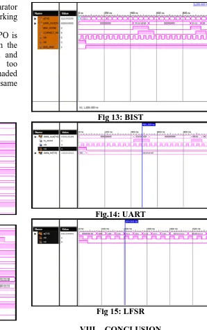
Fig 13: BIST
Fig.14: UART
Fig 15: LFSR
VIII. CONCLUSION
Available online: https://edupediapublications.org/journals/index.php/IJR/ P a g e | 901 relating information put away in the ROM. A change
can be made in the field of usage of the Test Response Analyser (TRA). As opposed to utilizing ROM as TRA, Multiple Input Shift Register (MISR) can be utilized for a similar reason. All the
reenactment result introduced in our paper
demonstrates that the BIST empowered UART is functioning admirably.
REFERENCES
1. M.S. Harvey,Generic UART Manual,Silicon
Valley,December 1999
2. P. J. Anderson, “The designer‟s guide to VHDL”
, Morgan Kaufman, 2nd edition, 2002.
3. K. Zarrineh, and S. J. Upadhyaya, “On
programmable memory built-in self-test
architectures”, Design, Automation and Test in Europe
4. Conference and Exhibition 1999. Proceedings,
1999, pp. 708 -713.
5. Dr. T.V.S.P. Gupta, Y. Kumari, M.Asok
Kumar”UART realization with BIST architecture
using VHDL” International Journal of