University of South Carolina
Scholar Commons
Theses and Dissertations
2016
Wireless Channel Modeling For Networks On
Chips
William Rayess
University of South Carolina
Follow this and additional works at:https://scholarcommons.sc.edu/etd Part of theElectrical and Electronics Commons
This Open Access Dissertation is brought to you by Scholar Commons. It has been accepted for inclusion in Theses and Dissertations by an authorized administrator of Scholar Commons. For more information, please [email protected].
Recommended Citation
Rayess, W.(2016).Wireless Channel Modeling For Networks On Chips.(Doctoral dissertation). Retrieved from
WIRELESS CHANNEL MODELING FOR NETWORKS ON CHIPS
by
William Rayess
Bachelor of Engineering Notre Dame University, 2008
Master of Communications Technology and Policy Ohio University, 2009
Submitted in Partial Fulfillment of the Requirements
For the Degree of Doctor of Philosophy in
Electrical Engineering
College of Engineering and Computing
University of South Carolina
2016
Accepted by:
David Matolak, Major Professor
Mohammod Ali, Committee Member
Paul Huray, Committee Member
Srihari Nelakuditi, Committee Member
ii
DEDICATION
Every challenging work needs dedicated self-efforts as well as guidance of people
whom we hold very closely to our hearts. I dedicate this dissertation to my father, my
mother, my brother, and my sister and her husband along with their lovely family of three
beautiful girls. Their constant words of encouragement that still ring in my ears helped
iv
ACKNOWLEDGEMENTS
I would like to express my deepest gratitude for my advisor Dr. David Matolak
for his full support, expert guidance, understanding, and encouragement throughout my
studies and research here at the University of South Carolina and also at Ohio University
where he had faith in my potential and admitted me to start my doctorate. This
dissertation would not have been possible without his patience, expertise, and
unwavering positive attitude even in the most challenging times. This experience has not
only been enriching on the academic level by getting exposed to ground-breaking
research but it has also molded my personality in a very positive manner rendering me a
more patient and resolute individual.
I would like to thank my committee members Dr. Mohamod Ali, Dr. Paul Huray,
and Dr. Srihari Nelakuditi, for their insightful comments, valuable input, and excellent
suggestions. I really appreciate the generosity of Dr. Paul Huray for allowing me to use
the Ansys cluster that allowed solving some of my demanding simulations. I also would
like to thank the WiNoC team at Ohio University comprised of Dr. Avinash Kodi, Dr.
Savas Kaya, and their Ph.D. students, who earned their Ph.D.’s, Dr. Dominic Di Tomaso
and Dr. Soumyasanta Laha. Collaborating with all of them has been a very enriching
experience especially learning about the other facets of the WiNoC project.
Many thanks go to my colleagues Dr. Ruoyu Sun, Hossein Ali Jamal, and Jinwen
collaboration on different projects helped broaden my knowledge in different areas and I
vi
ABSTRACT
The advent of integrated circuit (chip) multiprocessors (CMPs) combined with the
continuous reduction in device physical size (technology scaling) to the sub-nanometer
regime will result in an exponential increase in the number of processing cores that can
be integrated within a single chip. Today’s CMPs already support tens to low hundreds of
cores and both industry and academic roadmaps project that future chips will have
thousands of cores. Therefore, while there are open questions on how to harness the
computing power offered by CMPs, the design of power-efficient and compact on-chip
interconnection networks that connects cores, caches and memory controllershas become
imperative for sustaining the performance of CMPs.
As the limited scalability of bus-based networks degrades performance by
reducing data rates and increasing latency, the Network-on-Chip (NoC) design paradigm
has gained momentum, where a network of routers and links connects all the cores.
However, power consumption of NoCs is a significant challenge that should be addressed
to capitalize on the scaling advantages of multicores.
Also, improvements in metal wire characteristics will no longer satisfy the power
and performance requirements of on-chip communication. One approach to continue the
performance improvements is to integrate new emerging technologies into the electronic
design flow such as wireless/RF technologies, since they provide unique advantages that
make them desirable in a NoC environment. First, wireless technologies are ubiquitous
knowledge for the design and implementation of wireless chipsets using RF-CMOS
technology. Second, wireless communication, unlike wired transmission, can be
omnidirectional, which can facilitate one-hop unicast, multicast, and broadcast
communication that can result in a reduction in power consumption while allowing for
faster communication. Third, wireless communication can increase the communication
data rate by the combination of Frequency Division Multiplexing (FDM) and Time
Division Multiplexing (TDM) (and in the future, potentially spatial division multiplexing
(SDM)). Therefore, Wireless NoC (WiNoC) interconnects have recently emerged as a
viable solution to mitigate power concerns in the short to medium term while still
providing competitive performance metrics, i.e., low power consumption, tens of Gbps
data rates, and minimal circuit area (or volume) within the chip. Worth noting is that
wireless links are not envisioned as replacing all wired links, but rather as augmenting the
wired interconnection network.
In this dissertation, we employ simulations in HFSS from Ansys® to present
accurate wireless channel models for a realistic WiNoC environment. We investigate the
performance of these models with different types of narrowband and wideband antennas.
This entails estimation of the scattering parameters for the channels between multiple
antenna elements in the WiNoC, from which we derive channel transfer functions and
channel impulse responses. Using these results, we can estimate the throughput of the
various WiNoC links, and this allows us to design effective multiple access (MA)
schemes via FDM and TDM. For these MA schemes, we provide estimates of maximal
throughput. To further the feasibility study, we investigate the performance of a simple
viii
channels, which can facilitate one-hop unicast, multicast, and broadcast communication
that can result in a reduction in power consumption while allowing for faster
communication.
Our investigation of the performance of On-Off Keying modulation (OOK) also
includes an analytical expression for bit error ratio (BER) that can be evaluated
numerically. This enables us to provide the equalization requirements needed to achieve
our target BERs. Finally, we provide recommendations for WiNoC design and future
TABLE OF CONTENTS
DEDICATION ... iii
ACKNOWLEDGEMENTS ... iv
ABSTRACT ... vi
LIST OF TABLES ... xii
LIST OF FIGURES ... xiv
LIST OF ABBREVIATIONS ...xx
CHAPTER 1INTRODUCTION ...1
1.1OVERVIEW ON WIRED NETWORKS ON CHIPS ...1
1.2EXISTING ON-CHIP INTERCONNECT SOLUTIONS ...1
1.3SCALABILITY ...3
1.4WIRED NETWORK LIMITATIONS AND WINOCBENEFITS ...4
1.5SPECTRAL BANDS FOR WINOC’S ...7
1.6DISSERTATION OBJECTIVES ...9
1.7DISSERTATION CONTRIBUTIONS ...11
CHAPTER 2LITERATURE REVIEW ...14
2.1INTRA-CHIP ANTENNAS ...14
2.2INTER-CHIP ANTENNAS ...18
2.3CARBON NANOTUBES AND METAMATERIAL ANTENNAS ...20
x
CHAPTER 3SIMULATION DESCRIPTION ...27
3.1INTRODUCTION ...27
3.2FINITE ELEMENT METHOD ...28
3.3OTHER NUMERICAL METHODS IN HFSS ...34
3.4EXAMPLE RESULTS FROM HFSS ...37
CHAPTER 4MONOPOLE AND DIPOLE MODEL RESULTS ...39
4.1INTRODUCTION ...39
4.2MONOPOLE ANTENNA MODEL AND RESULTS ...39
4.3EXAMPLE LINK BUDGET ...44
4.4PRINTED DIPOLE MODEL AND RESULTS ...46
4.5COMBINED MONOPOLE/DIPOLE NETWORK RESULTS ...50
4.6DIPOLES WITHOUT GROUND PLANE MODEL RESULTS ...53
4.7MULTIPLE ACCESS ...56
CHAPTER 5WIDEBAND ANTENNAS ...63
5.1INTRODUCTION ...63
5.2HELICAL ANTENNA MODEL ...63
5.3DISCONE MODEL ...68
5.4BOWTIES MODEL ...73
5.5LOG-SPIRAL MODEL ...79
5.6WIDEBAND MULTIPLE ACCESS SCHEMES ...84
CHAPTER 6OOKBIT ERROR RATIO AS A FUNCTION OF CHANNEL IMPULSE RESPONSE ...96
6.1ANALYSIS ...96
6.3EQUALIZATION EFFECT ...107
CHAPTER 7CONCLUSIONS AND FUTURE WORK ...111
7.1DISSERTATION CONCLUSIONS ...111
7.2FUTURE WORK ...115
REFERENCES ...118
APPENDIX A–Verifying the Free Space Propagation Model in HFSS ...130
APPENDIX B–Verifying the Two- Ray Propagation Model in HFSS ...134
APPENDIX C–Effect of Insertion Loss slope variation on RMS Delay Spread ...142
xii
LIST OF TABLES
Table 1.1 WiNoC technology challenges in three potential frequency bands ...9
Table 2.1 Summary of WiNoC antenna characteristics from the literature ...25
Table 3.1 Comparison of Different Numerical Methods ...36
Table 3.2 Monopole dimensions ...37
Table 4.1 Maximum bandwidth channel allocation for monopole model ...59
Table 4.2 Maximum bandwidth channel allocation for printed dipole model ...62
Table 5.1 Maximum bandwidth channel allocation for helix model ...86
Table 5.2 Maximum bandwidth channel allocation for discone model ...88
Table 5.3 Maximum bandwidth channel allocation for bowtie model ...91
Table 5.4 Maximum bandwidth channel allocation for log-spiral model ...94
Table A.1 Difference between Analytical and Simulation Results for different distances at 600 GHz ...132
Table A.2 Difference between Analytical and Simulation Results for different distances at 60 GHz ...133
Table C.1 RMS-DS values for insertion loss curve of Figure C.1 ...143
Table C.2 Delay Spread for different Insertion Loss Phase and Amplitude Slopes ...145
Table D.1 Model dimensions at different center frequencies ...149
Table D.2 Maximum Bandwidth Channel Allocation for Model at f0= 75 GHz ...151
Table D.3 Maximum Bandwidth Channel Allocation for Model at f0= 150 GHz ...153
xiv
LIST OF FIGURES
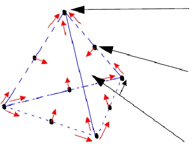
Figure 1.1 Mesh, Concentrated Mesh and Flattened Butterfly topologies ...2
Figure 1.2 Relative compute and interconnect energy scaling with technology ...7
Figure 3.1 Finite Element Mesh Example ...29
Figure 3.2 Representation of a Field Quantity in HFSS ...30
Figure 3.3 Adaptive Solution Process in HFSS ...34
Figure 3.4 HFSS interface with inset showing a “zoom in” of the monopole ...37
Figure 3.5 Return loss of HFSS example design monopole ...38
Figure 3.6 Azimuth (left) and Elevation(right) plane radiation pattern ...38
Figure 4.1 Monopole model. Bottom left: cross-section; upper left: top view showing monopoles near corners of chip; and, upper right: close-up top view of quarter wave monopole...40
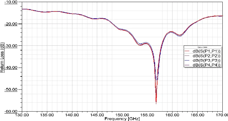
Figure 4.2 Return loss for the monopole design in dB (S(Pi,Pi) is 20log10(Sii), i=1,2, 3, 4 ...41
Figure 4.3 Insertion Loss for the monopole design in dB (S(Pi,Pj) is 20log10(Sij), i=2, 3, j=1 ...42
Figure 4.4 Unequalized power delay profiles of monopole channels in specific frequency band 150-160 GHz ...43
Figure 4.5 Monopole elevation radiation pattern at polar coordinate ...43
Figure 4.6 Monopole azimuth radiation pattern at polar coordinate ...44
Figure 4.7 Printed dipole model design showing cross section ...47
Figure 4.9 Insertion loss for printed dipole design in dB(S(Pi,Pj) is 20log10(Sij), i=2, 3,
j=1 ...48
Figure 4.10 Unequalized power delay profiles of printed dipole channels in a specific frequency band ...49
Figure 4.11 Printed dipole with ground plane elevation radiation pattern at polar coordinate ...49
Figure 4.12 Printed dipole with ground plane azimuth radiation pattern at polar coordinate ...50
Figure 4.13 Simulation model. Bottom left: cross-section; upper left: top view showing monopoles near corners of chip; and, upper right: close-up top view of quarter wave monopole...51
Figure 4.14 Insertion losses for various antenna pairs in the design of Figure 4.13 ...52
Figure 4.15 Unequalized power delay profiles of monopoles channels in different frequency bands ...53
Figure 4.16 Return loss for printed dipole design without a ground plane in dB (S(Porti,Porti) is 20log10(Sii), i=1, 2, 3, 4 ...54
Figure 4.17 Insertion loss for printed dipole design without a ground plane in dB (S(Porti,Portj) is 20log10(Sij), i=2, 3, j=1 ...55
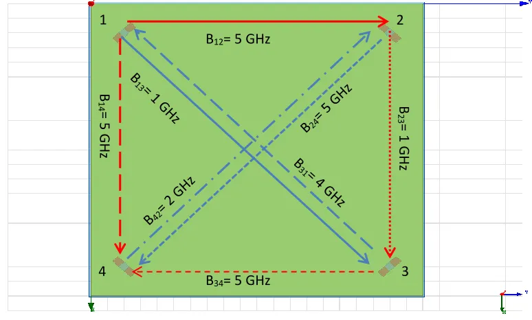
Figure 4.18 Insertion loss for monopole model with channel bandwidth ...57
Figure 4.19 Channel bandwidth for monopole design ...57
Figure 4.20 Channel assignment for monopole model ...58
Figure 4.21 Insertion loss for printed dipole model with channel bandwidths ...60
Figure 4.22 Channel bandwidths for printed dipole design ...61
Figure 4.23 Channel assignment for the printed dipole model ...61
xvi
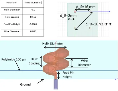
Figure 5.3 Insertion loss for helical antenna design in dB (St(Port_i,Port_j)) is
20log10(Sij), i=2, 3, j=1 ...66
Figure 5.4 Unequalized power delay profiles of helix channels in specific frequency band 150-160 GHz. ...67 Figure 5.5 Helix elevation radiation pattern at polar coordinate ...67
Figure 5.6 Helix azimuth radiation pattern at polar coordinate ...68
Figure 5.7 Discone model. Bottom: cross-section with inset table showing dimensions of the discone parameters; upper right: parameters of the discone; and, upper left: top view showing discones near corners of chip. ...69
Figure 5.8 Return loss for discone antenna design in dB (S (Porti,Porti)) is 20log10(Sii),
i=1, 2, 3, 4 ...70
Figure 5.9 Insertion loss for discone antenna design in dB (S (Porti,Portj)) is 20log10(Sij),
i=2, 3, j=1. ...71
Figure 5.10 Unequalized power delay profiles of discone channels in a specific frequency band. ...72
Figure 5.11 Discone elevation radiation pattern at polar coordinate ...72
Figure 5.12 Discone azimuth radiation pattern at polar coordinate ...73
Figure 5.13 Bowtie model. Bottom left: cross-section; bottowm right: table showing dimensions of the bowtie parameters; upper right: parameters of the bowtie; and, upper left: top view showing bowtie near corners of chip. ...74
Figure 5.14 Return loss for bowtie design in dB(S (Porti,Porti)) is 20log10(Sii), i=1, 2, 3,
4...75
Figure 5.15 Insertion loss for bowtie antenna design in dB (S (Porti,Portj)) is 20log10(Sij),
i=2, 3, j=1 ...76
Figure 5.16 Unequalized power delay profiles of bowtie channels in specific frequency band 140-150 GHz ...77
Figure 5.17 Bowtie elevation radiation pattern at polar coordinate ...78
Figure 5.19 Log-spiral model. Bottom left: cross-section; bottom right: table showing dimensions of the log-spiral parameters; upper right: parameters of the log spiral; and, upper left: top view showing bowtie near corners of chip ...79
Figure 5.20 Return loss for log-spiral design in dB(S (Porti,Porti)) is 20log10(Sii), i=1, 2,
3, 4...80
Figure 5.21 Insertion loss for log-spiral antenna design in dB (S (Porti,Portj)) is
20log10(Sij), i=2, 3, j=1 ...81
Figure 5.22 Unequalized power delay profiles of log-spiral channels in specific frequency band 150-160 GHz ...82
Figure 5.23 Log-spiral elevation radiation pattern at polar coordinate ...83
Figure 5.24 Log-spiral azimuth radiation pattern at polar coordinate ...83
Figure 5.25 Insertion loss for helix model with channel bandwidths per each 5 GHz channel ...84
Figure 5.26 Channel bandwidths for helix design ...85
Figure 5.27 Channel assignment for helix model ...86
Figure 5.28 Insertion loss for discone model with channel bandwidths for each of the 5 GHz channels ...87
Figure 5.29 Channel bandwidth for discone design...87
Figure 5.30 Channel assignment for discone model ...88
Figure 5.31 Insertion loss for bowtie model with channel bandwidth s for each of the 5 GHz channels ...89
Figure 5.32 Channel bandwidth for bowtie design ...90
Figure 5.33 Channel assignment for bowtie model ...90
Figure 5.34 Insertion loss for log-spiral model with channel bandwidths for each of the 5 GHz channels ...92
Figure 5.35 Channel bandwidth for log-spiral design ...93
xviii
Figure 6.2 Simulated and analytical probability of bit error vs. Eb/N0 for a 10 GHz “low
dispersion” discone diagonal channel ...102
Figure 6.3 Simulated and analytical probability of bit error vs. Eb/N0 for a 10 GHz
“highly dispersive” discone side channel ...103
Figure 6.4 Simulated and analytical probability of bit error vs. Eb/N0 for a 10 GHz “low
dispersion” log-spiral side-to-side channel ...104
Figure 6.5 Simulated and analytical probability of bit error for a 10 GHz “high dispersion” log-spiral diagonal channel ...105
Figure 6.6 Simulated and analytical probability of bit error vs. Eb/N0 for a 10 GHz “low
dispersion” monopole diagonal channel ...106
Figure 6.7 Simulated and analytical probability of bit error vs. Eb/N0 for a 10 GHz “high
dispersion” monopole side channel ...106
Figure 6.8 Simulated and analytical probability of bit error vs. Eb/N0 for a 10 GHz “high
dispersion” monopole side channel with equalization ...109
Figure 6.9 Simulated and analytical probability of bit error vs. Eb/N0 for a 10 GHz “high
dispersion” discone side channel with equalization ...110
Figure 6.10 Simulated and analytical probability of bit error vs. Eb/N0 for a 10 GHz
“high dispersion” log-spiral side channel with equalization ...110
Figure A.1 Path loss vs. distance, both simulated (dashed) and theoretical (solid) for 600 GHz frequency, two half-wavelength dipoles ...131
Figure A.2 Path loss vs. distance, both simulated (dashed) and theoretical (solid) for 60 GHz frequency, two half-wavelength dipoles ...132
Figure A.3Dipole radiation pattern in dBi ...133
Figure B.1 Two-ray ground reflection model ...134
Figure B.2 Path loss vs. distance, both simulated (solid) and theoretical (dashed) for 600 GHz frequency, two half-wavelength dipoles above an infinite PEC ground plane ...137
Figure B.3 Radiation pattern (elevation, dBi) for 600 GHz, two half-wavelength dipoles elevated 10 mm above an infinite PEC ground plane ...137
Figure B.5 Impulse response of a channel between two half-wavelength dipoles operating at 600 GHz at a height of 40 mm above an infininte PEC ground plane and a separation
of 75 mm ...140
Figure B.6 Impulse response of two half-wavelength dipoles operating at 600 GHz at height of 15 mm above an infininte PEC ground plane and at separation 150 mm ...141
Figure C.1 Insertion loss example ...142
Figure C.2 Phase of Insertion Loss ...145
Figure D.1 Monopole model simulated at 38 GHz ...147
Figure D.2 Insertion Loss at f0=38 GHz in dB (S(Pi,Pj) is 20log10(Sij), i=2, 3, j=1 ...148
Figure D.3 Channel bandwidth for the design at f0=38 GHz ...150
Figure D.4 Insertion Loss at f0=38 GHz in dB (S(Pi,Pj) is 20log10(Sij), i=2, 3, j=1 ...151
Figure D.5 Channel bandwidth for the design at f0=75 GHz ...152
Figure D.6 Insertion Loss for the monopole design in dB (S(Pi,Pj) is 20log10(Sij), i=2, 3, j=1 ...153
Figure D.7 Channel bandwidth for the design at f0=150 GHz ...154
Figure D.8 Insertion Loss at f0=300 GHz in dB (S(Pi,Pj) is 20log10(Sij), i=2, 3, j=1 ...155
Figure D.9 Channel bandwidth for the design at f0=300 GHz ...156
Figure D.10 Insertion Loss at f0=600 GHz in dB (S(Pi,Pj) is 20log10(Sij), i=2, 3, j=1 ....157
xx
LIST OF ABBREVIATIONS
AWGN ... Additive White Gaussian Noise
BER ... Bit Error Rate
BW ... Bandwidth
CIR ... Channel Impulse Response
C-MESH ... Concentrated Mesh
CMOS ... Complementary Metal Oxide Semiconductor
CMP ... Chip MultiProcessor
CNT... Carbon Nanotube
DFE ... Decision Feedback Equalizer
DFVS ...Dynamic Frequency and Voltage Scaling
EM... Electromagnetic
EMC ... Electromagnetic Coupling
EMI ... Electromagnetic Interference
ERC ...Error Correction Code
FDM ... Frequency Division Multiplexing
FEM ... Finite Element Method
FIFO ...First In First Out
HFSS ... High Frequency Structure Simulator
IE ... Integral Equation
ISI ... Inter Symbol Interference
MA ... Multiple Access
MaxSCBW ... Maximum Single Channel Bandwidth
MEMS ... Microelectromechanical Systems
MoM ... Method of Moments
MOSFET ... Metal Oxide Semiconductor Field Effect Transistor
MPC ... Multipath Component
MWCNT ... Multi-walled Carbon Nanotube
NOC ... Network on Chip
NSF ... National Science Foundation
OOK ... On Off Keying
PDP ... Power Delay Profile
RC ... Resistive-Capacitive
RCS ... Radar Cross Section
RF ... Radio Frequency
RF-CMOS ... Radio Frequency Complementary Metal Oxide Semiconductor
RFID ... Radio Frequency Identification
RMS-DS ... Root-Mean-Square Delay Spread
S2S ... Side to Side
SDM ... Spatial Division Multiplexing
SNR ... Signal to Noise Ratio
TDM ... Time Division Multiplexing
1
Chapter 1
Introduction
1.1 Overview on Wired Networks on Chips
The emergence of chip multiprocessors (CMPs) coupled with aggressive technology
scaling in the sub nanometer regime will result in a dramatic increase in the number of
cores, the processing units that read and execute instructions that can be integrated on a
single chip [1-3]. Some of today’s CMPs that employ tens to low hundreds of cores
include Intel’s 80-core TeraFlops processor [4], NVIDIA’s 512-core Fermi [5], Tilera’s
72-core CMP [6], and the 256-core programmable many-core Kalray [7]. In addition,
both academic and industry projections talk about future chips having thousands of cores
[1, 2, 7]. Therefore, the design of power-efficient1 and compact on-chip interconnection
networks plays a crucial role to harness the computing power offered by CMPs [8]. These
interconnection networks substantially affect the overall system performance.
1.2 Existing On-Chip Interconnect Solutions
The most prevalent approach to interconnecting multi-core CMPs is through
wired structures. Two dimensional meshes and rings are two common topologies that are
used, and they are suitable for planar silicon dies due to their low dimensionality (2D vs.
3D). The benefits of two dimensional meshes (Figure 1(a)) are the short wire lengths and
the low router complexity. This low complexity comes from the fact that a data packet
arriving at an intermediate router is forwarded to the next router until it reaches its
destination, typically according to a simple routing algorithm. However, the 2D mesh
network diameter, defined as the longest of the shortest path lengths from any node to
any other node, is proportional to the mesh size. For an NN mesh, the network diameter
is 2 (N1/2 - 1). Thus, meshes suffer from long network diameter, and this induces high
network latencies.
The concentrated mesh, shown in Figure 1.1 (b), reduces the total number of
network nodes by grouping multiple cores to share a network interface. For example, a
4-way concentration would lead to reducing the number of effective nodes by a factor of
4. Compared to the two dimensional mesh, the concentrated mesh has a smaller network
diameter and better resource sharing but still suffers from poor scalability. Due to
physical limitations that limit the degree of concentration, a concentrated mesh with for
example, 1024 cores with 4-way concentration would have a network diameter of 30
hops and consequently still high and undesirable network latency. A “hop” is defined as a
transition point that packets traverse on the path between source and destination.
(a) Mesh (b) Concentrated Mesh
3
Recent efforts [9] proposed at “flattening” what is known as a conventional butterfly
topology onto a two dimensional substrate. A butterfly topology consists of (k+1)2k nodes
arranged in k+1 ranks (rows), each containing n=2k nodes where k is the order of the
network. The resulting topology, referred to as a flattened butterfly (see Figure 1 (c)),
along with the concentration technique used in the concentrated mesh, reduces the
network diameter to only two hops. This can be achieved by using dedicated links to
connect the concentrated nodes in all dimensions. However, in this flattened butterfly
topology, the number of channels in each dimension increases quadratically with the
number of nodes present, leading to very complex wiring layouts. Moreover, long wires
connecting distant routers are undesirable since on-chip Resistive-Capacitive (RC) wires
require frequent repeaters to propagate signals over long distances in order to avoid
considerable signal level attenuation.
1.3 Scalability
Since it is only a matter of time until CMPs feature hundreds or thousands of
cores, it is important to consider how the aforementioned interconnect solutions will scale
when applied to CMPs with thousands of cores. In this context, minimizing the hop count
is essential since intermediate routers are a significant source of delay. In addition, long
wires are undesirable since on-chip RC wires require repeaters every few millimeters to
maintain a detectablesignal level over long wire spans. Thus, it is critical to see how the
above interconnect solutions fair when accommodating CMPs with several hundreds or
thousands of cores.
Even though simple ring arrangements are very cost effective, they are the least
number of cores. Most of the energy expenditure in Network on Chips ( NOC ) is due to
overcoming attenuation in channels, router FIFOs( first-in first-out ) buffers and router
crossbar (switch) fabrics. Meshes perform better as the hop count scales with the square
root of the mesh size. However, becausea very significant amount of latency and energy
is due to the intermediate router at each hop, it is clear that a more scalable solution is
needed. As for the concentrated mesh (C-mesh) topology, it represents a significant
improvement over the basic mesh by reducing the total effective node count and network
diameter; it also diminishes the area footprint of this topology by reducing the effective
node count by a concentration factor, k, and leads to better resource sharing. However,
the concentration factor is restricted due to physical limitations such as router cross bar
complexity and the size and energy required to support large numbers of input and output
ports and so a large network C-mesh does not scale very well, and would still exhibit
unacceptable network latency. On the other hand, even though low-diameter topologies
such as the flattened butterfly reduce the network diameter to two, the high number of
dedicated point to point links and long wires connecting distant routers cause complicated
wiring problems and high attenuations (yielding an energy penalty). This makes the
flattened butterfly topology also not very scalable since the link count increases
quadratically in each dimension with the number of cores. Hence, the flattened butterfly
topology is also not a very desirable topology for a thousand core network.
1.4 Wired Network Limitations and WiNoC Benefits
According to the International Roadmap for Semiconductors (ITRS),
5
offered by those metallic buses in addition to the RC delay caused by disproportionate
scaling of transistors [9]. Both limitations have led to the emergence of
Network-on-Chips architectures that employ shorter wires that improve throughput and reduce latency
[10-15]. However, power dissipation due to routers and links in addition to losses
incurred with lower technology node size can still cause bottlenecks for NoCs. In the
64-core Tilera mentioned earlier, it has been shown that NoCs consume 36 percent of total
chip power while routers alone consume 40 percent of the individual tile power coming
from core, cache, and router power. (A tile is an entity that combines a processor and its
associated cache in addition to a switch.) Even though the router in Intel’s Teraflops
processor employs several power efficient techniques, it still consumes 28 percent of tile
power, considerably higher than the targeted 10 percent of tile power [16]. Thus, as seen
in Figure 1.2, power dissipation is the biggest hurdle for the NoC paradigm, as agreed by
industry and academia [17, 18]. We can see from Figure 1.2 that at 45 nm, the
communication and computation energy are almost equal. At a technology size of 7 nm,
the computation energy decreases by a factor of 6 from that of the 45 nm technology, but
the interconnection energy only decreases by a factor of 1.6. Also at 7 nm, the
interconnection power is around 4 times that of the computation power. This means that
future chip designers have to make optimizing the power-performance efficiency of
communications a priority. To reduce power consumption, several concepts, such as
dynamic frequency and voltage scaling (DFVS) techniques [19, 20], topology
optimizations [21-23], router and crossbar optimizations [24-26], and encoding and
signaling techniques [27], have been proposed. However, these techniques come at a
optimization). Hence, the issues of power consumption, performance and area overhead
have to be addressed together in order to improve future CMP system performance.
In an effort to reduce power consumption in NoCs, new methods of integrating
emerging technologies have been proposed for the interconnection design of NoCs, such
as silicon nanophotonics [28-32], 3D integration [10, 33-35], and wireless/RF
technologies [36] . Although silicon nanophotonics and 3D interconnects have power and
performance advantages, they still face considerable technological (fabrication) barriers,
require innovative material advances and significant paradigm shifts in design. On the
other hand, relatively mature wireless technologies can provide unique advantages that
make them very desirable in a NoC environment. The first advantage that wireless
technologies bring is the wide range of options they provide in various communications
applications.
A large amount of information exists for the design and implementation of
wireless chipsets, utilizing RF-CMOS technology. Second, wireless communication
offers different degrees of flexibility in the spatial, temporal and frequency domains;
unlike wired transmission, wireless communication can be omnidirectional, which can
enable one-hop unicast, multicast and broadcast communication that can reduce power
utilization while yielding faster communication. Third, wireless interconnects can
increase the communication data rate by a combination of Frequency Division
Multiplexing (FDM), Time Division Multiplexing (TDM), and Spatial Division
Multiplexing (SDM). Subsequently,Wireless NoC (WiNoC) interconnects have as of late
7
ultrashort (1-10 mm) wireless separations with different multiplexing alternatives is not
trivial, given the high capacity required of wired interconnects (very high data rates, e.g.,
10 Gbps), the diverse inter-core traffic patterns involved, the number and dimensions of
antennas needed, and the often severe channel dispersion in the WiNoC environment.
Therefore, the focus of this dissertation is the wireless communication aspect of this
multi-faceted problem; the other two major research areas involved in this WiNoC
project are efficient transceiver circuits and devices, and computer architecture and
networking design. These areas have been investigated by our colleagues in this project.
Figure 1.2. Relative compute and interconnect energy scaling with technology [37].
1.5 Spectral Bands for WiNoC’s
In order for wireless links to truly enhance NoC performance, they must provide
high throughputs (e.g., tens of gigabits per second), utilize power- and area-efficient
transceivers, and employ efficient multiple access (MA) across the shared spatial
channel. Providing tens of gigabits per second among multiple cores is a challenging task
especially when frequency spectrum is limited. This limited spectrum is due to the fact
regulatory limitations. Although link distances are very short, wireless transceivers must
have minimal power consumption, and in the low mmwave frequency range, antennas
will be inefficient due to their small electrical size (required to physically fit on the chip).
The high data rate requirement also challenges circuit design, as most digital circuits
cannot currently operate at these rates, and required serial-parallel conversions may
introduce additional and unacceptable power consumption and complexity, so very
simple modulation/demodulation schemes may be required. Since spectrum is limited
(primarily by devices), time and frequency division must be used to allow sharing of the
wireless medium. Spatial-division multiplexing (SDM) can provide valuable spatial reuse
of time-frequency resources, but this is very challenging at millimeter wave frequencies
because of the small and simple antennas that must be employed.
Thus, trades among various options in the three design areas must be made, and
for this it is of interest to look at frequency bands higher than the millimeter wave bands.
Increasing the carrier frequencies would provide more bandwidth but also introduces
other challenges. In Table 1.1 [38] we provide a summary of these considerations in three
broad frequency bands. We considered the frequency bands in three broad categories:
circuits/devices, antennas/propagation, and system/architecture. The “best” band is not
obvious, although selecting the frequency band of 150–500 GHz may satisfy the largest
number of design criteria in the near term. It is clear that although a very challenging
task, to design and implement a complete solution for WiNoCs, all three design areas
9
Table 1.1. WiNoC technology challenges in three potential frequency bands [38].
Technology/Design Area
Frequency Band
50-150 GHz 150-500 GHz 500 GHz-3 THz
Circuits, Devices Status: currently feasible Technology: RF-CMOS, substrate SOI Status: encouraging Technology: SiGe-BiCMOS, substrate SOI Status: immature Technology: III-V/Si hybrid, substrate alumina Antennas, Propagation Status: very challenging Issues: electrically-small (inefficient) antennas, near field coupling Status: challenging Issues: nearing conventional antennas, far-field conditions Status: reasonable
Issues: at highest
f’s, propagation
analysis conventional, antennas immature
System, Architecture Issues: throughputs too low, SDM very difficult Area: Low-Q inductors, large antenna size Power: Manageable Issues: sufficient throughput, SDM challenging
Area: Very lossy substrates, ultra-low Q Power: challenging Issues: ample throughput, SDM possible
Area: limited by waveguides & sources
Power: Very challenging
1.6 Dissertation Objectives
In this section, a list of the dissertation objectives is presented.
1. [Chapter 2]: Perform a literature review of state of the art characterization of the
and antenna modeling and look at their performance in terms of bandwidth,
impedance matching, gain, and efficiency. Finally, we point out the gaps that we
fill in the dissertation.
2. [Chapter 3]: We present a description of the numerical methods that HFSS®, the
3-Dimensional software we use for our simulations and designs, uses and discuss
the advantages and disadvantages of each method. Finally, we show example
results for a monopole antenna including its return loss and radiation pattern.
3. [Chapter 4]: We present the first two types of simple antennas we simulated in
HFSS inside the WiNoC environment—quarter wavelength monopoles and
printed dipoles. We present results on the antenna themselves, such as return loss
and radiation pattern, in addition results for the wireless channels the
communication signals must traverse, in terms of insertion losses and dispersion
measures, which are critical to quantify for the design of efficient and reliable
wireless communication links. We also present results for the throughput of
frequency division multiple access schemes based upon the wireless channel (and
antenna) characteristics.
4. [Chapter 5]: We investigate and present results of inherently wideband antennas
inside the WiNoC environment. Similar to the treatment in chapter 4, we show
results on the antennas themselves and the wireless channels between them, in
addition to the throughput of frequency division multiple access schemes based
upon the wireless channel characteristics.
5. [Chapter 6]: We investigate, through an analysis, the performance of a basic
11
and find an analytical expression for BER that can be evaluated numerically. We
also present the performance improvements attainable with equalization of highly
dispersive channels that exhibit bit error rate floors.
6. [Chapter 7]: Summarize the dissertation and indicate future work.
1.7 Dissertation Contributions
The project “Power-Efficient Reconfigurable Wireless Network-on-Chips (NoC)
Interconnects for Future Many-core Architectures” was funded by the National Science
Foundation (NSF) - ECCS Division, and began in September 2011. The research group
consists of a collaborative effort between two Ohio University faculty members and their
students and my advisor Dr. David Matolak and myself. The group has three journal
publications and seven conference publications; I am an author on the three journal
papers and four of the six conference publications. The notations J and C used in the
following list denote journal paper and conference paper, respectively. Ultimately, our
contribution in this dissertation is the illustration of practical WiNoC channel, antenna,
and communication link performance characteristics, along with observations and results
useful for future research in this area.
[J1] D. DiTomaso, A. Kodi, D. W. Matolak, S. Kaya, S. Laha, and W. Rayess,
“A-WiNoC: Adaptive Wireless Network-on-Chips (NoCs) Architecture for Future
Multicores,” IEEE Transactions on Parallel and Distributed Systems, vol. 26, no. 12, pp.
3289 – 3302, December 2015.
[J2] S. Laha, S. Kaya, D. W. Matolak, W. Rayess, D. DiTomaso, and A. Kodi, “A New
Interconnects,” IEEE Transactions on Computer-Aided Design of Integrated Circuits and
Systems, vol. 34, no. 2, pp. 186-198, February 2015.
[J3] D. Matolak, A. Kodi, S. Kaya, D. DiTomaso, S. Laha, and W. Rayess, “Wireless
Networks-on-Chips: Architecture, Wireless Channel, and Devices,” IEEE Wireless
Communications Magazine, Special Issue on Wireless Communications at the Nanoscale,
October 2012.
[C1] M.A.I, Sikder, A. Kodi, D. DiTomaso, S. Kaya, W. Rayess, D. Matolak., "Exploring
Wireless Technology for Off-Chip Memory Access”, IEEE 24th Annual Symposium on
High-Performance Interconnects (HOTI, Aug. 2016
[C2] A. Kodi, A. Sikder, D. DiTomaso, D. W. Matolak, S. Kaya, S. Laha and W.
Rayess, “Kilocore Wireless Network-on-Chips (NoCs) Architecture,” 2nd ACM
International Conference on Nanoscale Computing and Communication (NanoCom),
Boston, Massachusetts, 21-22 September 2015.
[C3] S. Kaya, S. Saha, D. DiTomaso, A. Kodi, D. W. Matolak, and W. Rayess, “On
Ultra-short Wireless Interconnects for NoCs and SoCs: Bridging the ‘THz Gap’,” 56th
IEEE International Midwest Symposium on Circuits & Systems (MWSCAS), Columbus,
Ohio, 4-7 August 2013.
[C4] D. DiTomaso, A. Kodi, D. Matolak, S. Kaya, S. Laha, and W. Rayess,
“Energy-efficient Adaptive Wireless NoCs Architecture,” 7th International Symposium on
13
Other Project Conference Papers (on which I am not a co-author)
[C4] S. Laha, S. Kaya, A. Kodi, D. DiTomaso, and D. Matolak, “A 60 GHz tunable LNA
in 32 nm Double Gate MOSFET for a Wireless NoC Architecture,” IEEE Wireless and
Microwave Technology Conference, 7-9 April 2013.
[C5] D. DiTomaso, S. Laha, A. Kodi, S. Kaya, and D. Matolak, “Evaluation and
Performance Analysis of Energy Efficient Wireless NoC Architecture,” 55th
International Midwest Symposium on Circuits and Systems, Boise, Idaho, 5-8 August
2012.
[C6] D. DiTomaso, S. Laha, S. Kaya, D. Matolak, and A. Kodi, “Energy-Efficient
Modulation for a Wireless Network-on-Chip Architecture,” 10th IEEE International
NEWCAS Conference, Montreal, Canada, 17-20 June 2012.
I also have a publication under review in the Wireless Personal Communications Journal:
W. Rayess, D. W. Matolak, S. Kaya, A. Kodi, “Antennas and Channel Characteristics for
Chapter 2
Literature Review
We have divided this review into three categories: intra-chip antennas, inter-chip
antennas, and papers that deal with carbon nanotubes and metamaterials. The first
category is directly applicable to WiNoCs; the second may be suitable if the structures
can be modified (reduced in size); and the third category represents more novel or
speculative designs. Table 2.1 contains a summary of the results from the literature
review.
2.1 Intra-Chip Antennas
As a result of rapidly expanding applications for sensor networks, Radio
Frequency Identification (RFID) tags and system-on-chip integration, intra-chip antennas
have recently drawn attention. In [39], the authors analyzed several antenna structures
and produced simulation results for transmission gain at microwave frequencies.
Although these frequencies are too low for most WiNoC applications, we provide results
for completeness. The transmission gain is the decibel sum of transmit and receive
antenna gains plus the path gain; when measured it is essentially the scattering parameter
S21, which quantifies gain from port one to port two. As expected, meander, zigzag, and
folded structures showed higher gains than linear dipoles (all structures are planar,
15
gains and channel attenuations from these transmission gain values, since this requires an
assumption for the path gain (or loss). Thus our antenna gain estimates cited
throughoutare of limited accuracy, since we employ only the very simplest of path loss
models, but the relative gain values among the different antenna types is accurate. The
transmission gain for the linear dipole pair in [39] was between approximately -70 to -50
dB for the frequency range 1-8 GHz with maximum gain occurring near 6 GHz. The
meander dipole had a gain between 10-15 dB larger, with the peak value occurring at
around 5.8 GHz, and the folded dipole had a gain between 0 and 25 dB larger than the
dipole, with its peak value occurring near 6.5 GHz. If we employ the free space loss
model, the transmission gains cited would yield maximum antenna gains of
approximately -16.9, -13.9, and -24.3 dB for the meander, folded dipole, and linear
dipole, respectively. The size of these antennas ranged from 8-9 mm and the link distance
was 4.7 mm, hence far-field conditions are not attained for our (absolute) antenna gain
estimates. The simulations in [39] were done using Sonnet® Suites™.
In [40], the authors investigated the effect on the transmission properties of an
on-chip dipole antenna when a diamond layer was inserted between a silicon substrate and
its heat sink. The size of the antenna simulated in HFSS was 2 mm. The range of
simulation frequencies was 5-40 GHz. The transmission gain of the on-chip dipole
antennas was estimated for different link distances. It was concluded that a higher gain
could be achieved with a diamond layer (0.35 mm thick) atop the substrate than without
the layer. Transmission gain was largest from 15-40 GHz with the 0.35 mm thick
diamond layer; link distance was less than 3 mm. The corresponding antenna gain,
be -7.9 dB. With a higher resistivity substrate (100 Ω-cm), the corresponding antenna
gain would be -2.9 dB. A complication here again is that the link distance of 1 mm is not
in the far field at 26 GHz—nonetheless, the relative antenna gain between the cases is
accurate. Additional impedance matching networks are needed in the configuration in
[40] since throughout the simulation, the resistances were above 50 ohms. In addition,
adding a diamond layer would increase the overall chip implementation cost and
complexity.
The authors in reference [41] investigated meander antennas with different
pitches, lengths, widths, and numbers of turns. These antennas are printed conductors that
resemble “square wave” shapes fabricated on a P-type SiO2 substrate. HFSS was used to
conduct simulations. The authors found that increasing the pitch length and number of
turns while decreasing the antenna width did increase the radiation efficiency. Table 2.1
has additional specifications.
In a very early paper in the field, the authors of [42] investigated short linear,
meander, and zigzag dipole antennas experimentally. These antennas were formed on a
silicon wafer. Table 2.1 summarizes results. In [43], two kinds of antennas were realized,
the inverted-F and dipole. Their characteristics were also investigated via simulations
(HFSS) and are shown in Table 2.1.
In [44], the author investigated the effect of using a metamaterial crystal substrate
within the dielectric layer on which a rectangular microstrip patch antenna was mounted.
This reference employs simulations (CST Microwave Studio) to determine antenna
17
references [45]-[47] report on designs in the high mm-wave and sub-THz frequency
ranges.
The authors of [48] compared the performance of a dipole antenna pair with a
phased array pair for on-chip communication. The array consisted of four orthogonal
quarter wave monopole linear arms that are fed differentially. Their simulations were
done using CST Microwave Studio, with results again in Table 2.1.
Reference [49] described a WiNoC in which printed zig-zag antennas are used.
The authors discussed at length the required connectivity and routing, but also described
the main antenna features. Antenna gains were approximately -18.5 dB with a center
frequency near 63 GHz.
Reference [50] presented four designs for on chip antennas operating at 90 GHz
and 140 GHz, and compared their performance; see Table 2.1. The antennas were a
bowtie-shaped slot antenna, a cavity-backed slot antenna, an extremely flat waveguide
slot antenna, and an E-shaped patch antenna.
The authors of [51] designed, fabricated and measured the performance of a dual
band Buckled Cantilever Plate triangular fractal antenna on flexible polyamide at 60 GHz
and 77 GHz. The movable plate enables horizontal and vertical polarization on the same
chip. An increase of 6 dB in gain was observed in the vertical position compared to the
2.2 Inter-Chip Antennas
Due to the availability of unlicensed bands in the 60-90 GHz range for several
upcoming applications such as vehicular radars and in-room multimedia links, as well as
commercially available RF-CMOS processes in the mm-wave regime, inter-chip antennas
are also relevant for the WiNoC problem. For instance, reference [52] reported on results
using an ultra wide band triple “twiggy” antenna that was developed using 65 nm
complimentary metal-oxide semiconductor (CMOS) technology. No explicit antenna
parameters were provided.
In [53] the authors proposed the design of a two-antenna array at 60 GHz for
chip-to-chip communication, with simulations done using HFSS. Despite the fact that the
array antenna offers an increase in gain of 5 dB in the horizontal direction over a single
antenna, a crucial characteristic not reported in [53] is the physical size of these antennas.
A similar design in [54] consists of a four-element array that achieves 8 dB increase in
gain over the single antenna in the diagonal direction with a 30 GHz bandwidth at 60
GHz.
In [55], a dielectric waveguide with a high dielectric constant was used under a
silicon chip to improve the efficiency and transmission gain of the on-chip antenna.
Efficiency and gains were investigated as functions of the silicon resistivity and
thickness. The gain increased with a thinner silicon substrate. Efficiency and transmission
gain improvements of 50% and 25 dB, respectively, were seen at a transmission distance
of 20 mm with the thinner substrate. Thus the paper notes an important fabrication point
19
semiconductor field-effect transistor (MOSFET) gate stacks may also be used as the top
insulator/passivation layers before the antennas are fabricated.
Reference [56] presents results for different patch antennas that were designed
with various gap configurations; simulated values of return loss were provided. Two of
the five types of patch antennas with different gap configurations were fabricated, and the
experimental results showed a difference of 1.5 GHz in the resonant frequency between
measurements and simulations. A worst case transmission gain of -47 dB for a
chip-to-chip link of distance 35 mm yields an estimate of approximately -3.75 dB for the antenna
gain (again assuming free space).
The authors of [57] designed a wireless inter-chip link using bond-wire antennas.
The chip was fabricated using 180 nm SiGe technology. Data rates of 2 to 6 Gbps were
achieved over distances from 0.5 to 4 cm, at a center frequency of 43 GHz. Antenna
gains were measured to be approximately -1.4 dB.
In [58], the authors reviewed the use of on-chip antennas for over the air
communication and presented ways to increase communication range. To achieve this,
the authors suggest using 6 mm monopole antennas operating at 5.8 GHz instead of 3 mm
dipole antennas operating at 24 GHz in addition to thinning the silicon substrate below
the antennas from 670 µm to 100 µm. Note that decreasing the operating frequency
increases range naturally, but also generally has the undesirable effect of reducing
bandwidth. The antenna gains are highly dependent on their height from the ground
plane; for example, gains drop by 20 dB when the height decreases from 52 cm to 5 mm.
whereas in the thinner substrate case, the on-chip 24 GHz dipole and 5.8 GHz monopole
gains are -7 dB and -11 dB, respectively. Interested readers who would like more insight
on this topic are referred to [59].
2.3 Carbon Nanotubes and Metamaterial Antennas
Reference [60] is a nice overview paper on the properties of carbon nanotubes. It
shows that nanotubes have very unique electrical, mechanical, thermal, and optical
properties, which make them very good candidates for on chip antennas. Fabricating
them in a scalable manner and integrating them with CMOS circuits is though currently
expensive and challenging, hence we present these results as a potential future option for
WiNoC antenna design.
The authors of [61] have some interesting results, with good radiation patterns for
plasmonic antennas. One issue is that these plasmonic antennas must be illuminated by a
laser beam to resonate. This consumes substantial power, and this is problematic in
WiNoC systems that aim to be as power efficient as possible.
In [62] the authors show some promising results for multi-walled carbon
nanotubes (MWCNTs). Again, required excitation through a laser would consume a
considerable amount of energy, disadvantageous in a NoC environment. Also, the high
temperatures used to grow the MWCNT’s could make it very challenging to integrate
these structures with CMOS devices.
Reference [63] explored antennas for a relatively low frequency range (up to 10
21
may be questionable especially when the process of fabricating these antennas involves
temperatures as high as 720 degrees Celsius.
Another interesting paper on Carbon Nanotubes (CNTs) is [64], in which the
authors describe the use of CNT “forests” for antennas. A very nice analysis is performed
for OOK performance, but for the applications described, the center frequency is
extremely low (~15 MHz), which limits data rates to below 1 Mbps.
2.4 Additional Remarks
From Table 2.1 we can draw several conclusions regarding WiNoC antenna design:
1. research to date has been focused on microwave and low-millimeter wave frequencies,
which is likely not high enough to support future WiNoC data rates.
2. most antenna gains found in the literature, except for [44], [49], [53],and [53] are less
than 0 dB, which means that the antenna adds losses to the transmission.
3. printed antenna structures are most common, with non-monotonic effects vs. frequency
for substrate thickness.
4. impedance matching of the antenna to the transceiver/transmission line is often
required, although exceptions exist, e.g., in [59] a co-design approach canceled the need
for a matching network by optimizing the antenna and IC for conjugate matching.
However, when present, matching networks still occupy valuable WiNoC transceiver
5. antenna efficiencies may be very low (part of this may be attributable to impedance
mismatching), which means that additional transmission power is required compared to
the impedance-matched case.
6. reported results for transmission gain obscure the specification of antenna gain itself,
making antennas used within such transmission gain results not “portable” to other
physical settings.
7. reported bandwidths are in many cases larger than our minimum estimated bandwidth
of 10 GHz, which is promising.
Given the novelty of the WiNoC environment, for WiNoC antennas, we may need to
deviate from conventional antenna theory meant for 3D far-field communication since
the actual WiNoC antenna requirements differ substantially from those used in
conventional designs. It is our belief that the challenges in WiNoC antennas also provide
unique opportunities to design novel on-chip antennas using perhaps revolutionary
innovations in nanotechnology and nanomaterials. Some of these solutions are very likely
to broaden the concept of on-chip antennas significantly, and some rely on novel
materials (e.g., [39]), unique insights on nanotechnology, and micro integration. What
follows is a non-exhaustive list of ideas that we have found in the literature for novel
compact antenna designs. Such ideas would be very valuable in the future design and
23
Inductive Coupling: commonly used for power transmission over short
distances, laterally and vertically coupled inductances may be used to
communicate between the closest transceivers [65].
Metamaterials: as also suggested by [39], metamaterials designed for mm wave
performance can be used to isolate and focus radiation, especially in the higher
bands of interest. They may also be used to reduce the antenna size, especially in
the higher end of the frequency range considered, i.e., the THz regime.
Pulse-Driven Antennas: although only demonstrated for HF transmission [66]
thus far, the idea of actual pulses driving antennas without impedance matching is
a very promising and intriguing possibility for WiNoCs, as it can further reduce
area/power requirements and minimize circuitry required for modulation.
Plasmonic (Yagi-Uda) Antennas: plasmonics, another by-product of
nanophotonics and nanomaterials, provide extremely novel radiation mechanisms
to enable electromagnetic radiation using plasmon coupled waves on metal
nanostructures. A recent paper on this idea [67] claims that the concept can be
extended to THz radiation, and this would be a very promising way to build
compact antennas with moderate gain.
Bonding-wire Antennas: another unique possibility for WiNoCs is the use of
existing bond wires at the perimeter of the chip as antennas for on-chip
communication (e.g., [57]). While this would require unique optimizations to the
geometry of the wires and an infrastructure to (de)-couple radiation, it is possible
MEMS/3D Structures: over the last 20 years, the Microelectromechanical
Systems (MEMS) community has amassed many CMOS compatible fabrication
options to build folding/assembling 3D (strictly speaking 2.5D) metal structures
that can reach 100’s of microns in length [68]. It may be possible to borrow ideas
to build folded or vertical antenna structures that can liberate area constraints
substantially.
2D reflectors/directors: on-chip antennas can benefit from planar and/or
vertically stacked reflector/director metal structures (once again built using
largely MEMS technology) to improve the antenna directivity and efficiency.
Actually, this would be easier to implement for planar structures than fully 3D
cases in conventional large antennas.
While some of these ideas and concepts may be difficult and challenging to
implement in a WiNoC environment, an innovative combination of these ideas will
be needed to bring the sought after performance promised by WiNoCs. Promising and
rapid advancements in technology would be very helpful in bringing these methods
and ideas into fruition and facilitating the actual manufacturing of the WiNoC
components and landscape. Moreover, these innovative concepts would allow to
extract the performance gains that WiNoCs present in future multi core chips and
25
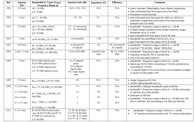
Table 2.1. Summary of WiNoC antenna characteristics from the literature
Ref Antenna Size
Bandwidth B, Center Freq fc
Frequency Range f
Antenna Gain (dB) Impedance () Efficiency Comments
[39] 8.9 mm f= 1.8 GHz fc= 4 GHz
-16.9, -13.9, -24.3 N/A N/A Gains: meander, folded dipole, linear dipole, respectively
Gains estimated from free-space (not in far field)
Simulation results (Sonnet) [40] 2 mm f= 5 – 40 GHz
fc= 25 GHz
-7.9, -2.9 ~75 N/A Gain estimated from free-space for 10-cm, 100-cm substrates, respectively, each w/0.35 mm diamond layer beneath (not in far field)
[41] 2.9 mm f=1-12.4 GHz (VNA) f=1-20 GHz (HFSS) fc= 10 GHz
-27- -21 (measured) -14 - -22 (simulated)
N/A 3-6 % bandwidth ~ frequency range in which S11 < -10 dB
multiple designs yielded several smaller frequency ranges, bandwidth up to 11.4 GHz
gain estimated from free-space (not in far field [42] 2 mm f=6-18 GHz, fc= 12 GHz -19 (meander) ~150 N/A bandwidth not quantified in terms of S11 or S21
gain estimated from free-space (not in far field) [43] 0.45 mm B
1=14 GHz, fc= 60 GHz
B2=7 GHz, fc= 60 GHz
-8 (inverted F) -14 (dipole)
50 9% (inverted-F) 2% (dipole)
bandwidth ~ frequency range in which S11 < -10 dB
inverted-F ~51-65 GHz; dipole ~58-65 GHz [44] 1 mm × 1 mm B=120 GHz, fc= 800 GHz 8.25 at 852 GHz matched with
feed
88.3 % at 852 GHz
bandwidth ~ frequency range in which S11 < -10 dB
resonates at 693.45, 797.4, and 852 GHz
size is 2D since patch antenna [48] 4 mm B=8.5 GHz (dipole pair)
B=25 GHz (phased array) fc= 16 GHz (dipole pair) fc= 22 GHz (phased array)
-11.51 (phased array) -21.6 (aligned
dipole pair) -32.2 (opp. dipole
pair)
N/A N/A bandwidth ~ frequency range in which S11 <-10 dB
dipole pair 14.5-23 GHz, resonating at ~16 GHz, phased array resonating at ~22 GHz
2 dipole length 4 mm; array of four /4 monopoles arranged in square of side length 2 mm
[49] 0.3 mm B
3dB=16 GHz, fc= 62.5 GHz 3.9 N/A N/A Center frequency 62.5 GHz 16 GHz 3dB bandwidth from S21
[50] 1.4 x 0.9 mm
1.2 x 0.6 mm
0.6 x 2 mm
0.7 x 0.7 mm
B3dB=72-120 GHz, fc= 90 GHz
B= 5 GHz, B3dB=20 GHz, fc= 140 GHz
B3dB= 3 GHz, fc=140 GHz
B=10 GHz, fc= 140 GHz
-1.5 -1.4 -1 -2 N/A 50 50 50 N/A N/A N/A N/A
bandwidth is 3dB gain bandwidth; peak at 90 GHz
bandwidth ~ frequency range in which S11 <-10 dB, resonating
at 140 GHz; B3dB=136-156 GHz
peak gain at 140 GHz
bandwidth ~ frequency range in which S11 <-10 dB, from 138
GHz to 148 GHz, and resonating at 141 GHz and 146 GHz
[51] 2 x 2.3 mm B=50-85 GHz for horizontal case, B=60-65 GHz and B =75-85 GHz for vertical case fc= 60 GHz
-3( “H” & 60 GHz) 3.5 (“V” & 60 GHz) -2.1 (“H” & 77 GHz) 4.8 (“V” & 77 GHz)
N/A N/A bandwidth ~ frequency range in which S11 <-10 dB
2.5 Gaps in the WiNoC Literature
Most of the papers in the literature focus on antennas, as mentioned earlier in the
remarks, operating in the microwave and low-millimeter wave range. In order to deliver
the high throughput and data rates required by WiNoC’s, antennas should be operating at
much higher frequencies in order to benefit from the higher bandwidth available in that
part of the spectrum. It is understandable that the technology to fabricate such structures
is still immature and if even possible, it would be very expensive. Also, the fabrication of
RF components, such as oscillators and amplifiers, operating at such high frequencies,
remains very challenging.
As for WiNoC wireless channel modeling, the vast majority of papers found in
the literature use very simplistic models—mostly the free space model. This is a gross
simplification since the WiNoC landscape is complex, with different layers of substrates
and metals that the electromagnetic waves, travelling between transmitting and receiving
antennas, interact with. Therefore, more precise models are imperative in order to better
27
Chapter 3
Simulation Description
3.1 Introduction
Computer techniques have revolutionized the way electromagnetic (EM)
problems are analyzed. Radio Frequency (RF) and microwave engineers rely heavily on
computer simulations to analyze and help evaluate new designs or design specifications.
Although most EM problems consist of solving a set of partial differential equations
subject to specific boundary conditions, very few practical problems can be solved
without the aid of a computer or cluster of machines.
Computer methods for analyzing problems in electromagnetics generally are
divided into two categories --analytical techniques or numerical techniques. Analytical
techniques make simplifying assumptions about the geometry of a problem in order to
apply a closed-form or tabulated solution. Numerical techniques attempt to solve
fundamental field equations directly, subject to the boundary conditions set by the
geometry.
Numerical techniques generally require more computation than analytical
techniques, but they are very powerful EM analysis tools. Without making assumptions
about which field interactions are most significant, numerical techniques analyze the
entire geometry provided as input. They calculate the solution to a problem based on a