65
Design and Implementation of FAM based Optimized
Modified Booth Recoder
Y.Ramesh
1, E.Adinarayana
2M.Tech Scholar, Dept. of ECE, Sri Mittapalli College Of Engineering, Guntur1 Associate Professor Dept. of ECE, Sri Mittapalli College Of Engineering, Guntur2
Email: Email: [email protected], [email protected]
Abstract- Complex arithmetic operations are widely used in Digital Signal Processing (DSP) applications. In this work, we focus on optimizing the design of the fused Add-Multiply (FAM) operator for increasing performance. We investigate techniques to implement the direct recoding of the sum of two numbers in its Modified Booth (MB) form. We introduce a structured and efficient recoding technique and explore three different schemes by incorporating them in FAM designs. Comparing them with the FAM designs which use existing recoding schemes, the proposed technique yields considerable reductions in terms of critical delay, hardware complexity and power consumption of the FAM unit. This paper aims at additional reduction of latency and area of the Wallace tree multiplier. This is accomplished by the use of Booth algorithm and compressor adders. The coding is done in Verilog HDL and synthesized for Xilinx Virtex 6 FPGA device.
Keywords:Add-Multiply operation, arithmetic circuits, Modified Booth recoding, VLSI design, Arithmetic, Booth Encoder, Compressors, Radix-8, and Wallace-Tree.
1. INTRODUCTION
A multitude of various multiplier architectures have been published in the literature, during the past few decades. The multiplier is one of the key hardware blocks in most of the digital and high performance systems such as digital signal processors and microprocessors. With the recent advances in technology, many researchers have worked on the design of increasingly more efficient multipliers. They aim at offering higher speed and lower power consumption even while occupying reduced silicon area. This makes them compatible for various complex and portable VLSI circuit implementations [2].However, the fact remains that the area and speed are two conflicting performance constraints. Hence, innovating increased speed always results in larger area. The proposed architecture enhances the speed performance of the widely acknowledged Wallace tree multiplier when implemented on a FPGA. The structural optimization is performed on the conventional Wallace multiplier, in such a way that the latency of the total circuit reduces considerably. The conventional Wallace tree multiplier architecture comprises of an AND array for computing the partial products, a carry save adder for adding the partial products so obtained and a carry propagate adder in the final stage of addition. In the proposed architecture, partial product generation and reduction is accomplished by the use of Booth recoding algorithm, 3:2, 4:2,and 5:2 compressor
66 Targeting an optimized design of AM operators,
fusion techniques [10]–[13], [23] are employed based on the direct recoding of the sum of two numbers (equivalently a number in carry-save representation [14]) in its Modified Booth (MB) form [15]. Thus, the propagate (or carry-look-ahead) adder [16] of the conventional AM design is eliminated resulting in considerable gains of performance. Lyu and Matula [10] presented a signed bit MB recoder which transforms redundant binary inputs to their MB recoding form. A special expansion of the preprocessing step of the recoder is needed in order to handle operands in carry-save representation. In [12], the author proposes a two-stage recoder which converts a number in carry-save form to its MB representation. The first stage transforms the carry-save form of the input number into signed-digit form which is then recoded in the second stage so that it matches the form that the MB digits request. Recently, the technique of [12] has been used for the design of high performance flexible coprocessor architectures targeting the computationally intensive DSP applications [17]. Zimmermann and Tran [13] present an optimized design of [10] which results in improvements in both area and critical path. In [23], the authors propose the recoding of a redundant input from its carry-save form to the corresponding borrow-save form keeping the critical path of the multiplication operation fixed. Although the direct recoding of the sum of two numbers in its MB form leads to a more efficient implementation of the fused Add-Multiply (FAM) unit compared to the conventional one, existing recoding schemes are based on complex manipulations in bit-level, which are implemented by dedicated circuits in gate-level. This work focuses on the efficient design of FAM operators, targeting the optimization of the recoding scheme for direct shaping of the MB form of the sum of two numbers (Sum to MB – S-MB). More specifically, we propose a new recoding technique which decreases the critical path delay and reduces area and power consumption. The proposed S-MB algorithm is structured, simple and can be easily modified in order to be applied either in signed (in 2’s complement representation) or unsigned numbers, which comprise of odd or even number of bits. We explore three alternative schemes of the proposed S-MB approach using conventional and signed-bit Full Adders (FAs) and Half Adders (HAs) as building blocks.
used to provide accurate measurements of area utilization, critical path delay and power dissipation regarding various bit-widths of the input numbers. We show that the adoption of the proposed recoding technique delivers optimized solutions for the FAM design enabling the targeted operator to be timing functional (no timing violations) for a larger range of frequencies. Also, under the same timing constraints, the proposed designs deliver improvements in both area occupation and power consumption, thus outperforming the existing S-MB recoding solutions.
2. EXISTING STRUCTURE
67
Fig. 1 Existing architecture
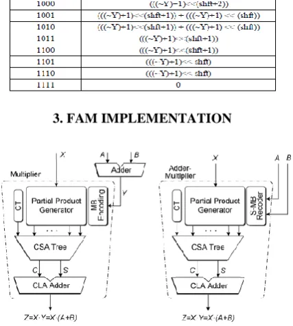
3. FAM IMPLEMENTATION
Fig.2 AM operator based on the (a) conventional design and (b) fused design with direct recoding of the sum of A and B in its MB representation. The multiplier is a basic parallel multiplier based on the MB algorithm. The terms CT, CSA Tree and CLA Adder are referred to the Correction Term, the Carry-Save Adder Tree and the final Carry-Look-Ahead Adder of the multiplier.
[image:3.595.76.267.99.289.2]Fig. 3 (a) Boolean equations and (b) gate-level schematic for the implementation of the MB encoding signals
Fig. 4 Generation of the ith bit Pji of the partial product PPj for the conventional MB multiplier
In the FAM design presented in Fig. 2(b), the multiplier is a parallel one based on the MB algorithm. Let us consider the product X.Y. Both X and Y consist of n=2k bits and are in 2’s complement form.
The generation of the i-th bit Pj,i of the partial product PPj is based on the next logical expression while Fig. 4 illustrates its implementation at gate level [20], [24]:
After the partial products are generated, they are added, properly weighted, through a Wallace Carry-Save Adder (CSA) tree [21] along with the Correction Term (CT) which is given by the following equations:
4. SUM TO MODIFIED BOOTH RECODING TECHNIQUE (S-MB)
[image:3.595.319.520.117.276.2] [image:3.595.72.286.384.622.2]68 two least significant of them has positive weight.
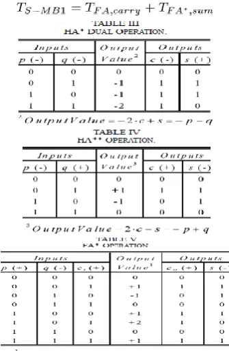
[image:4.595.73.276.102.501.2]Consequently, in order to transform the two aforementioned pairs of bits in MB form we need to use signed-bit arithmetic. For this purpose, we develop a set of bit-level signed Half Adders (HA) and Full Adders (FA) considering their inputs and outputs to be signed.
[image:4.595.320.520.104.297.2]Fig. 5 Boolean equations and schematics for signed (a) HA* and (b) HA**
Fig. 6 Boolean equations and schematics for signed (a) FA* and (b) FA**
4.2 Proposed S-MB Recoding Technique
We use both conventional and signed HAs and FAs in order to design and explore three new alternative schemes of the S-MB recoding technique. Each of the three schemes can be easily applied in either signed (2’s complement representation) or unsigned numbers which consist of odd or even number of bits.
1) S-MB1 Recoding Scheme: The first scheme of the proposed recoding technique is referred as S-MB1 and is illustrated in detail in Fig. 6 for both even (Fig. 6(a)) and odd (Fig. 6(b)) bit-width of input numbers. As can be seen in Fig. 6, the sum of and is given by the next relation:
Fig. 7 S-MB1 recoding scheme for (a) even and (b) odd number of bits
[image:4.595.335.503.466.723.2]69 2) S-MB2 Recoding Scheme: The second
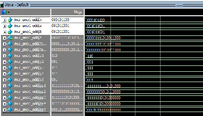
approach of the proposed recoding technique, S-MB2, is described in Fig. 7 for even (Fig. 8(a)) and odd (Fig. 8(b)) bit-width of input numbers. We consider the initial values C0,1=0 and C0,2=0.
The critical path delay of S-MB2 recoding scheme is calculated as follows:
Fig. 8 S-MB2 recoding scheme for (a) even and (b) odd number of bits
3) S-MB3 Recoding Scheme: The third scheme implementing the proposed recoding technique is S-MB3. It is illustrated in detail in Fig. 9 for even (Fig. 9(a)) and odd (Fig. 9(b)) bit-width of input numbers.
Fig. 9 S-MB3 recoding scheme for (a) even and (b) odd number of bits
The critical path delay of S-MB3 recoding scheme is calculated as follows:
4) Unsigned Input Numbers: In case that the input numbers A and B are unsigned, their most significant bits are positively signed. Figs. 10–12 present the modifications that we have to make in all S-MB schemes for both cases of even (the two most significant digits change) and odd (only the most significant digit change) bit-width of and , regarding the signs of the most significant bits of A and B. The basic recoding block in all schemes remains unchanged.
[image:5.595.89.279.99.257.2] [image:5.595.320.542.100.301.2] [image:5.595.74.280.295.516.2]70
Fig. 12 Implementation of the MSD of the S-MB3 recoding scheme in case of unsigned input numbers for (a) even and (b) odd bit-width
The Multiplier-Accumulator (MAC) operation is the key operation not only in DSP applications but also in multimedia information processing and various other applications. As mentioned above, MAC unit consist of multiplier, adder and register/accumulator. In this paper, we used 8 bit modified booth S-MB multiplier. The MAC inputs are obtained from the memory location and given to the multiplier block. This will be useful in 8 bit digital signal processor. The input which is being fed from the memory location is 8 bit. When the input is given to the multiplier it starts computing value for the given 8 bit input and hence the output will be 8 bits. The multiplier output is given as the input to carry save adder which performs addition.
5. SIMULATION RESULTS
[image:6.595.328.511.100.211.2]In Figs. 13 and 14 we present a comparison among all FAM designs, in terms of area and power consumption respectively, for even bit-width. For each case that we explored, we focus on the lowest clock period where all FAM designs are synthesized.
Fig. 13 Area comparison for even bit-width with all values normalized to the corresponding ones of [12]
[image:6.595.74.283.133.232.2]Fig. 14 Power comparison for even bit-width with all values normalized to the corresponding ones of [12]
[image:6.595.314.521.246.701.2]Fig. 15 S-MB1 even multiplication waveform
Fig. 16 S-MB1 odd multiplication waveform
[image:6.595.320.520.263.385.2] [image:6.595.318.524.420.538.2] [image:6.595.84.269.546.654.2] [image:6.595.321.519.575.697.2]71
[image:7.595.75.280.100.222.2]Fig. 18 S-MB2 odd multiplication waveform
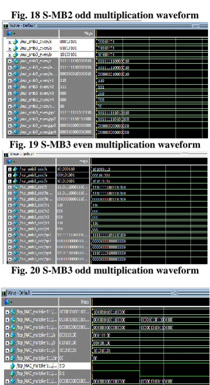
Fig. 19 S-MB3 even multiplication waveform
Fig. 20 S-MB3 odd multiplication waveform
Fig. 21 Mac output waveform
5. CONCLUSION
This paper focuses on optimizing the design of the Fused-Add Multiply (FAM) operator. We propose a structured technique for the direct recoding of the sum of two numbers to its MB form. We explore three alternative designs of the proposed S-MB recoder and compare them to the existing ones [12], [13] and [23]. The proposed recoding schemes, when they are incorporated in FAM designs, yield considerable performance
improvements in comparison with the most efficient recoding schemes found in literature. Hence a design of high performance 16 bit Multiplier-and-Accumulator (MAC) is implemented in this paper.
REFERENCES
[1] A. Amaricai, M. Vladutiu, and O. Boncalo, “Design issues and implementations for floating-point divide-add fused,” IEEE Trans. Circuits Syst. II– Exp. Briefs, vol. 57, no. 4, pp. 295–299, Apr. 2010. [2] E. E. Swartzlander and H. H. M. Saleh, “FFT
implementation with fused floating-point operations,” IEEE Trans. Comput., vol. 61, no. 2, pp. 284–288, Feb. 2012.
[3] J. J. F. Cavanagh,Digital Computer Arithmetic. NewYork:McGraw- Hill, 1984.
[4] S. Nikolaidis, E. Karaolis, and E. D. Kyriakis-Bitzaros, “Estimation of signal transition activity in FIR filters implemented by a MAC architecture,” IEEE Trans. Comput.-Aided Des. Integr. Circuits Syst., vol. 19, no. 1, pp. 164–169, Jan. 2000. [5] O. Kwon, K. Nowka, and E. E. Swartzlander, “A
16-bit by 16-16-bitMAC design using fast 5: 3 compressor cells,” J. VLSI Signal Process. Syst., vol. 31, no. 2, pp. 77–89, Jun. 2002.
[6] L.-H. Chen, O. T.-C. Chen, T.-Y.Wang, and Y.-C. Ma, “A multiplication- accumulation computation unit with optimized compressors and minimized switching activities,” in Proc. IEEE Int, Symp. Circuits and Syst., Kobe, Japan, 2005, vol. 6, pp. 6118–6121.
[7] Y.-H. Seo and D.-W. Kim, “A new VLSI architecture of parallel multiplier–accumulator based on Radix-2 modified Booth algorithm,” IEEE Trans. Very Large Scale Integr. (VLSI) Syst., vol. 18, no. 2, pp. 201–208, Feb. 2010.
[8] A. Peymandoust and G. de Micheli, “Using symbolic algebra in algorithmic level DSP synthesis,” in Proc. Design Automation Conf., Las Vegas, NV, 2001, pp. 277–282.
[9] W.-C. Yeh and C.-W. Jen, “High-speed and low-power split-radix FFT,” IEEE Trans. Signal Process., vol. 51, no. 3, pp. 864–874, Mar. 2003. [10] C. N. Lyu and D. W. Matula, “Redundant binary Booth recoding,” in Proc. 12th Symp. Comput. Arithmetic, 1995, pp. 50–57.
[11] J. D. Bruguera and T. Lang, “Implementation of the FFT butterfly with redundant arithmetic,” IEEE Trans. Circuits Syst. Il, Analog Digit. Signal Process., vol. 43, no. 10, pp. 717–723, Oct. 1996. [12] W.-C. Yeh, “Arithmetic Module Design and its
Application to FFT,” Ph.D. dissertation, Dept. Electron. Eng., National Chiao-Tung University,, Chiao-Tung, 2001.
[13] R. Zimmermann and D. Q. Tran, “Optimized synthesis of sum-of-products,” in Proc. Asilomar Conf. Signals, Syst. Comput., Pacific Grove, Washington, DC, 2003, pp. 867–872.
[image:7.595.71.281.225.609.2]72
[17] S. Xydis, I. Triantafyllou, G. Economakos, and K. Pekmestzi, “Flexible datapath synthesis through arithmetically optimized operation chaining,” in Proc. NASA/ESA Conf. Adaptive Hardware Syst., 2009, pp. 407–414.
[18][Online].Available:
http://www.synopsys.com/Tools/Implementation/ RTLSynthesis/DCUltra/Pages/default.aspx [19][Online].Available:
http://www.synopsys.com/Tools/Implementation/ SignOff/PrimeTime/Pages/default.aspx
[20] Z. Huang, “High-Level Optimization Techniques for Low-Power Multiplier Design,” Ph.D., University of California, Department of Computer Science, Los Angeles, CA, 2003.
[21] C. S. Wallace, “A suggestion for a fast multiplier,” IEEE Trans. Electron. Comput., vol. EC-13, no. 1, pp. 14–17, 1964.
[22] M. Daumas and D. W. Matula, “A Booth multiplier accepting both a redundant or a non-redundant input with no additional delay,” in Proc. IEEE Int. Conf. on Application-Specific Syst., Architectures, and Processors, 2000, pp. 205–214.
[23] Z. Huang andM. D. Ercegovac, “High-performance low-power left-toright array multiplier design,” IEEE Trans. Comput., vol. 54, no. 3, pp. 272–283, Mar. 2005.
[24].Young-Ho Seo and Dong-Wook Kim, "New VLSI Architecture of Parallel Multiplier-Accumulator Based on Radix-2 Modified Booth Algorithm," IEEE Transactions on very large cale integration (vlsi) systems, vol. 18, no. 2,february 20 10 [25]. Ron S. Waters and Earl E. Swartzlander, Jr., "A
Reduced Complexity Wall ace Multiplier
Multiply Accumulate Unit," IEEE International Conference on Emerging Trends in Engineering and Technology, ICETET-09
[28]. B.Ramkumar, Harish M Kittur and P.Mahesh Kannan, "ASIC Implementation of Modified Faster Carry Save Adder ", European Journal of Scientific Research, Vol. 42, Issue 1, 2010.
[29]. R.UMA, Vidya Vijayan, M. Mohanapriya and Sharon Paul, "Area, Delay and Power Comparison of Adder Topologies", International Journal of VLSI design & Communication Systems (VLSICSj Vo1.3, No.1, February 2012
[30]. V. G. Oklobdzija, "High-Speed VLSI Arithmetic Units: Adders and Multipliers", in "Design of High-Performance Microprocessor Circuits", Book edited by A.Chandrakasan,IEEE Press,2000
[31]. Dadda, "Some Schemes for Parallel Multipliers," Alta Frequenza, vol. 34, pp. 349-356, 1965
[32]. C.S. Wall ace "A Suggestion for a fast multipliers," IEEE Trans. Electronic Computers, vol. 13, no.l,pp 14-17, Feb. 1967
[33]. L.Dadda, "On Parallel Digital Multiplier", Alta Frequenza, vol. 45, pp. 574-580, 1976
[34]. WJ. Townsend, E.E. Swartzlander Jr., and J.A. Abraham, "A Comparison of Dadda and Wall ace Multiplier Delays," Proc. SPIE, Advanced Signal Processing Algorithms, Architectures, and Implementations XIII, pp. 552-560, 2003