Design of Low Pin Count Scan Architecture
5
0
0
Full text
Figure
![Fig 1 The impact of compression ratio on pattern count, test time and length of channel [7]](https://thumb-us.123doks.com/thumbv2/123dok_us/751936.1086478/1.595.301.528.566.767/fig-impact-compression-ratio-pattern-count-length-channel.webp)
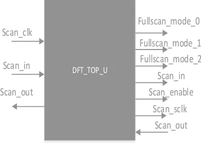
![Fig 6 Scan compression technique [8]](https://thumb-us.123doks.com/thumbv2/123dok_us/751936.1086478/4.595.123.245.482.566/fig-scan-compression-technique.webp)

Related documents