Implementation of Efficient Wallacetree
Multiplier
Sindhu M 1, Sandesh kumar B V 2
P.G. Student, Department of Electronics and communication engineering, SJBIT, Bangalore, Karnataka, India1
Assistant Professor, Department of Electronics and communication Engineering, SJBIT, Bangalore, Karnataka, India2
ABSTRACT: Low power consumption is an important concern for the VLSI circuit designers.Since 70% of
instructions in microprocessor and most of DSP algorithms perform addition and multiplication.As a result of expanding signal processing applications, the demand of high speed multipliers is increasing. Since the common multiplication method use shift and add algorithm.Optimization of adder is required to improve the performance of multiplier. In this work,we propose a modified full adder using multiplexer to achieve low power consumption of multiplier.Designs are developed using verilog HDL and functionalities are verified through simulation using xilinx14.6 and are synthesized in cadence RTL compiler using TSMC180nmtechnology.
KEYWORDS:Wallacetree multiplier,Fulladder,Multiplexer.
I. INTRODUCTION
Multipliers play an significant role in todays digital signal processing and other applications.High speed,low power consumption and hence delay are all the time be an essential design targets for any chip designer.As most of DSP structures include multipliers in their design.With the advances in technology,researchers are trying to decrease the delay of multiplier so that the delay of entire circuit can be reduced.Number of partial products to be added is the main parameter that determine the performance of multiplier.To reduce the number of partial products and achieve speed improvement ,Wallace tree multiplier is the most popular technique.It involve ANDing of multiplier and multiplicand bits for the generation of partial products in the first stage. In second stage full adders and half adders has been use for the reduction of partial products in two rows.Followed by addition of two rows using fast carry adders in the third stage.
This work mainly deal with the replacement of full adders with modified full adder in the reduction phase of the Wallace tree multiplier.In the preferred method, a modified full adder using multiplexer is useful to attain power reduction compare to the existing techniques with a small area and delay improvement
II.RELATEDWORK
A Typical Wallace Tree Multiplier
The Wallace tree multiplier is faster than array multipliers, since the delay in an array multiplier varies linearly, whereas in Wallace it varies logarithmically.Consider a N bits multiplication, N2 AND gates are required in order to produce the partial product terms and the number of reduction stages is given by S which is shown in (1)
Fig1Typical Wallacetree Multiplier
Fig1 shows 8-bit typical Wallace multiplier .It multiplies multiplicand and multiplier bits to generate the partial product in first stage.In second stage,when there are three bits,fulladders are used and for two bits ,halfadders are used.If there is any bit left in the column is passed to the next stage without processing.The final two rows are added using fast adder.
B. Using Regular Full adder
Fig 2.Regular Fulladder
Regular Wallace tree multiplier uses full adder in its reduction phase. Due to XOR gates;fulladder consumes more power. As shown in fig.2 regular full adder consists of two XOR gates in critical path of sum and one XOR gate, one AND gate and one OR gate in the critical path of the carry.Hence the critical path delay is given.
C. Fulladder using two 4:1multiplexers
Fig.3 Fulladder using two 4:1multiplexers
In sequence to reduce the power and area, the fulladder in reduction phase of Wallace tree multiplier is replaced by a modified full adder. In MUX based full adder, the fulladder is implemented using 4:1 multiplexers as shown in fig. 3.By implementing MUX based full adder in reduction phase of Wallace tree multiplier power reduction has been achieved. It is clear that, one 4:1 MUX can be made using three 2:1 MUX. The critical path delay can be written as shown.
Delay=Not+2*Mux
D. Fulladder using six 2:1Multiplexers
Fig.4 Fulladder using six 2:1 Multiplexers
Here, fulladder is designed using six 2:1multiplexers.Since each multiplexer is made using six transistors, totally twelve transistors are essential for the operation of full adder circuit. Most of the power consumption in any circuit is short circuit current, leakage current and logic transition. In this circuit, there is no direct connection between vdd and vss. So, the possibility of direct path occurrence between source and ground will be avoided which results in reduction in short circuit power. In addition to that, all the internal nodes are excited by fresh inputs, switching activity will also be reduced. This causes reduction in power but at thecost of area increment. Therefore critical path delay is given by
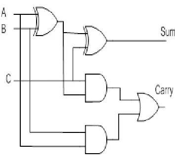
D Preferred Fulladder
Fig.4 Preferred Fulladder
This preferred fulladder consists of two 2:1multiplexers and xor gate.In this preferred technique,xor gate in fulladder is replaced by multiplexer block.As most of the power consumption is due to xor gates, by reducing number of xor gates ,power reduction can be achieved.This modified fulladder will be applied to Wallace multiplier
This modified expression for sum can be implemented by using first multiplexer and xor gate.
In Wallace multiplier structure,partial products are divided into definite stages. In each stage, whenever there are three bits, full adder has to be used. Out of the three inputs, one input and its complement are given as inputs to the first multiplexer.The other two will be given as input to xor gate,output of which will as select line for both the multiplexers.The bits other than carry bit are used inputs to the second multiplexer.This results in reduction in switching activity and also critical path delay compared to existing techniques.
Function of this modified fulladder as follows: a)If both B and C are zero or one,sum=A. b)If either of B or C is one and another is zero,sum=
A̅
. c)If either of B or C is one and another is zero,carry=A d)If both B and C are zero or one, carry= B.III. EXPERIMENTAL RESULTS
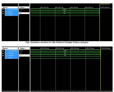
Here,Wallace multiplier designs are developed using verilog HDL for 8 and 16bits and are verified through simulations using Xilinx ISE.The simulation waveforms of Wallace multiplier using modified fulladder for both 8 and 16bit are shown in Figures 5,6.And these multiplier designs are synthesized in cadence RTL compiler using TSMC 180nm technology
.
Simulation waveforms
Fig5 :Simulation waveform for8bit Preferred Fulladder Wallace multiplier
Table 1:Comparsion based on area,power and delay
IV.CONCLUSION
By including modified fulladder in reduction stage of Wallace multiplier,an average area,power and delay reduction will be obtained.The synthesis results show that the preferred wallace multiplier is suitable for low power and small area applications.
REFERENCES
[1] C. Wallace, “A suggestion for a fast multiplier,” IEEE Transaction on Electronic Computers, Vol. EC-13, pp.14-17.
[2] R. S. Waters, E. E. Swartzlander, “A reduced complexity Wallacemultiplier reduction,” IEEE Transactions on Computers, vol. 59, no. 8, pp.1134-1137, 2010.
[3] Shahzad Asif and Yinan Kong, “Low Area Wallace Multiplier,” VLSI Design, vol. 2014.
[4] M. J. Rao, S. Dubey, “A high speed and area efficient Booth recoded Wallace tree multiplier for Fast Arithmetic Circuits,” in Asia Pacific Conferenceon Postgraduate Research in Microelectronics and Electronics(PrimeAsia), Hyderabad, India, 5-7 Dec. 2012, pp.220-223.
[5] Karthick, S. Karthika and S. Valannathy, “Design and Analysis of LowPower Compressors,” International Journal of Advanced Research in Electrical, Electronics and instrumentation Engineering, YoU, Issue 6,Dec. 2012.
[6] S. T. Oskuii, P. G. Kjeldsberg, “Power optimized partial product reduction interconnect ordering in parallelmultipliers,” NORCHIP, Aalborg, 19-20Nov. 2007, pp.1-6.
[7] M. V. P. Kumar, S. Sivanantham, S. Balamurugan, P. S. Mallick, “Low power reconfigurable multiplier with reordering of partial products,” inInternational Conference on Signal Processing, Communication, Computing and Networking Technologies (ICSCCN), Thuckafay, 21-22 July 2011, pp.532-536.