RANGING SENSOR
Thesis submitted for
the Degree of Master of Science
by
W e n Xin Huang, B. Sc.
Department of Applied Physics
Faculty of Science
I wish to express my thanks to Professor David Booth for the opportunity to undertake postgraduate research in the Department of Applied Physics and his m u c h appreciated encouragement.
I must thank my supervisors, Dr. Stephen Collins and Dr. Michael Murphy, for their counsel and support throughout this project. M a n y thanks also to Alex Shelamoff for his assistance and guidance with the electronics.
I wish to acknowledge the technical staff (Umit Erturk, Tibor Kovacs, Hayrettin Arisoy and M a r k Kivinen) for their engineering/electronic support. Special thanks
to Dr. Jakub Szajman, Neil Caranto and Charles K a d d u for their help in the v a c u u m laboratory. .Also the help from the staff and post-graduate students in the Department of Applied Physics was appreciated.
Contents
Contents Chapter 1 1.1 1.2 1.3 IntroductionFibre optic sensors Project aim
S u m m a r y of thesis contents
page
1.1 1.1 1.2
Chapter 2 Fibre optic sensing systems
2.1 2.2 2.2 2.4 2.5 2.6
Chapter 3 Review of ranging techniques
3.1 Introduction 3.1 3.2 Distance measurements by visual means 3.1
3.3 Non-optical distance measurements 3.2 3.4 Range measurements based o n laser and optical fibre
techniques 3.4 3.4.1 Time of flight 3.5
3.4.2 Phase shift measurement 3.5
3.4.3 Coherent F M C W 3.7 3.4.4 Incoherent F M C W 3.12
3.5 S u m m a r y 3.16 2.1 2.2 2.2.1 2.2.2 2.2.3 2.3 Introduction System components Light sources Optical fibres Photodetectors
Chapter 4 Theoretical analysis
4.1 Introduction 4.1 4.2 Fourier analysis of F M C W ranging 4.1
4.2.1 T h e beat waveform expression 4.1 4.2.2 Production of the beat note 4.3 4.2.3 Frequency analysis of the beat signal 4.4
4.2.4 Examination of the spectrum 4.6 4.2.5 Determination of the beat frequency 4.11
4.3 Noise in electrical circuits 4.12
4.3.1 Thermal noise 4.12 4.3.2 Shot noise 4.12 4.3.3 Signal-to-noise ratio (SNR) 4.13
4.3.4 S u m m a r y 4.15
Chapter 5 Experimental details
5.1 Introduction 5.1 5.2 Laser diode source 5.2
5.2.1 Laser diode source and modulation circuit 5.2 5.2.2 Modulation optimisation for the laser diode circuit 5.4
5.3 Photodetector circuit 5.6 5.4 Frequency response of the combined source and detector
system 5.8 5.5 Voltage-controlled oscillators (VCOs) 5.9
5.5.1 Attenuators for the V C O output 5.11 5.6 Optical fibres and directional coupler 5.13
5.7.1 Collimators 5.15 5.7.2 Reflectors 5.15 5.8 Electrical processing of detector output 5.16
5.8.1 Bandpass filters 5.16 5.8.2 Pre-amplifier 5.18 5.8.3 Electrical signal processor 5.19
5.9 Tektronix oscilloscope 5.27
Chapter 6 Experimental results
6.1 Introduction 6.1 6.2 Electrical simulation 6.1
6.3 Optimisation of the optical coupling efficiency of the
experimental system 6.5 6.4 Range determination from the modulation envelope 6.9
6.5 Range determination from the beat frequency 6.15 6.5.1 Range measurements using a T y p e 9036 V C O 6.16 6.5.2 Range measurements using a VTO-9032 V C O 6.19 6.6 Range measurements w h e n an anti-reflection ( A R ) coating
is present o n the fibre tip in the target path 6.24 6.6.1 Effect of the signal returned from the fibre tip of the target
path 6.24 6.6.2 Range measurements 6.28
6.7 Conclusion 6.31
Chapter 7 Final conclusion and future work
7.1 Final conclusion 7.1 7.2 Future w o r k 7.1
References Rl
Chapter 1 Introduction
1.1 Fibre optic sensors
Fibre optic sensors are relatively new devices that are finding applications in a n u m b e r of areas and, have b e c o m e possible due to the advances in fibre optic
technology (Dakin and Culshaw, 1988). In operation, the light guided within an optical fibre is modified in response to an external physical, chemical, or electromagnetic influence, which m a y change the intensity, phase, frequency, or polarisation of the light. C o m p a r e d to other sensing systems, fibre optic sensors have well-recognised advantages such as:
* Immunity from electromagnetic interference * Electrical isolation
* Chemical passivity
* Small size and low weight
* High sensitivity and the ability to interface with a wide range of measurands * M o r e information-carrying capacity (ie. greater bandwidth)
1.2 Project aim
The aim of this project was to construct and evaluate a fibre optic sensor for the non-contact measurement of range through the air. The sensor developed,
resolution of several cm was achieved. Possible applications of this sensor include the ullage of inflammable fluids in storage vessels, vehicle ranging for automatic braking schemes, robotics, machine vision a n d structure monitoring. For these applications, a straightforward and inexpensive device which is potentially mass-produced, would be desirable.
1.3 Summary of thesis contents
The basic components required in fibre optic sensors and the factors affecting optical coupling efficiency in such systems are discussed in Chapter 2. There
follows in Chapter 3 a review of existing ranging techniques, where different methods are described and their advantages and disadvantages are discussed.
The operating principles of the sensor under investigation, including a Fourier analysis of the sensor signal and its signal to noise ratio (SNR), are given in
detail in Chapter 4. Chapter 5 introduces all the optical and electrical components w h i c h were designed and used, including their performance characteristics.
Chapter 2 Fibre optic sensing systems
2.1 Introduction
Fibre optic sensors were introduced earlier (section 1.1) and may be classified simply in terms of where optical modulation occurs in the sensing loop. That is, if light propagates along a fibre to a n external modulator before being recaptured b y a second (or the s a m e ) fibre, it is called a n extrinsic sensor. Alternatively if the light responds to the measurand whilst still being guided, it is k n o w n as an intrinsic sensor (Fig 2.1).
* \
measurand
J
/
Intrinsic Extrinsic
Fig 2.1 Intrinsic and extrinsic fibre optic sensing system
In general, optical fibre based ranging schemes are extrinsic unless properties of optical fibres are to be investigated (Dakin and Culshaw, 1988). In the w o r k
presented in this thesis, an air path is involved and so the sensor developed w a s extrinsic (section 5.1).
Fibre optic components, of relevance to the ranging sensor developed, are briefly discussed in this chapter.
optical
fibre
A
measurand j2.2 System components
2.2.1 Light sources
Semiconductor light sources (laser diodes (LD) and light-emitting diodes (LED)) are the most important sources for fibre optic communication and sensing
systems (Palais, 1984). Their small size and adequate radiance are compatible with the diameter of fibres, and their compact solid structure and low-power requirements are suitable for modern solid-state electronics. Furthermore, their amplitude or frequency m a y be modulated easily by an appropriate change in bias current. T h e choice of light sources depends u p o n the intended
(Dakin and Culshaw, 1988). Single frequency laser diodes such as a distributed feedback (DFB) laser diode have longer coherence lengths (typically ~1 m ) but are very expensive. Bragg gratings are used to select the operational wavelength which is determined by the grating spacing. The spectra for single-mode and multimode laser diodes are compared in Fig 2.2
A Single mode
V)
c
CO
y
a
O
laser diode -0.1 nm
Multimode iaser diode
Wavelength Wavelength
Fig 2.2 Spectra of typical single-mode and multimode laser diodes
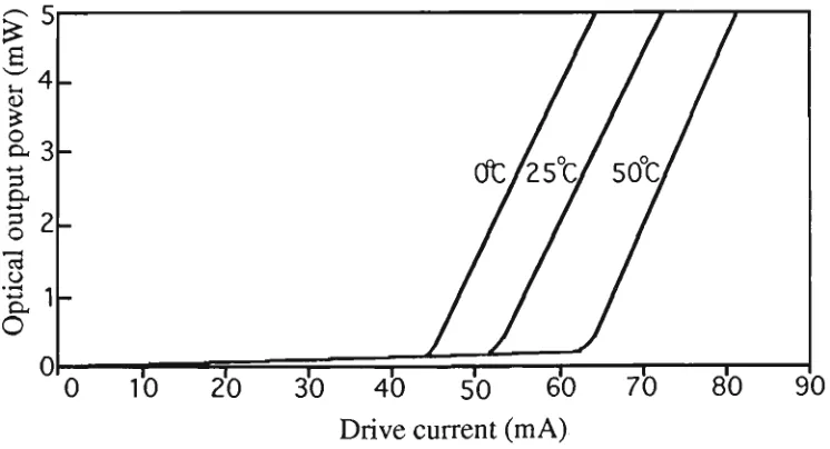
The relationship between the optical output power and drive current of the laser diode used in this project (section 5.2.1) is given in Fig 2.3. H o w e v e r , laser diodes are very sensitive to temperature, which affects the threshold current (Fig 2.3) and shifts the operational wavelength (Fig 3.3). Since u n w a n t e d temperature changes m a y distort modulated signals, a feedback element such as a thermoelectrical cooler m a y be necessary.
30 40 50 60 Drive current ( m A )
90
L D s are edge emitting, and a typical radiation pattern is s h o w n in Fig 2.4. C o m p a r e d to an L E D , the light from an L D is confined within a m u c h smaller angular spread, and so can be coupled more efficiently into an optical fibre. In this work, an inexpensive (less than A$10), single m o d e C D player L D w a s used (section 5.2.1).
0i = 10° (plane parallel to the junction) 82 = 35° (plane perpendicular to the junction)
Fig 2.4 Typical radiation pattern of a laser diode
222 Optical fibres
There are essentially three types of optical fibres; single-mode, multimode step index and multimode graded index (Palais, 1984). Single-mode fibres d o not
suffer from m o d a l dispersion but their power transmittance is limited. In multimode fibres the modulation bandwidth for a specific length is limited by modal dispersion, but greater power transfer is possible than in the single-m o d e case.
coupling efficiencies of single-mode fibres are m u c h lower than for multimode fibres since their core diameter is reduced (8 u m compared to 50 u m ) . In this work, 50/125 u m graded-index multimode silica fibre (~ $1/metre) w a s selected
(section 5.6.1), because the optical power transmission had to be maximised.
2.2.3 Photodetectors
Important photodetector characteristics are their responsivity, spectral response and rise time (Palais, 1984). There are five types in c o m m o n use, namely
v a c u u m photodiodes, photomultipliers and semiconductor pn, P I N and avalanche photodiodes (APD). V a c u u m photodiodes are not suitable for fibre sensing, and although photomultipliers ( P M T ) are fast and have high gain, their cost, size, weight and high bias voltage m a k e them inappropriate for fibre sensing systems.
this w o r k the carrier wavelength being detected w a s 780 n m , and so a P I N silicon photodiode w a s selected (section 5.3).
2.3 System coupling efficiency
Often, in a fibre sensing system, light must be coupled from a light source to a fibre, or from a fibre to a detector and so losses are inevitable. The losses in
coupling light into a fibre are due to the Fresnel end-reflection, and core and numerical aperture ( N A ) mismatches. Coupling efficiency depends o n the radiation pattern (Fig 2.4) of the source and the N A of the fibre (section 2.2.2) (Palais, 1984). Lenses or fibre pigtailed sources can be used to improve the coupling.
Losses also occur in mechanical fibre to fibre connections and are caused by lateral, longitudinal and angular misalignment and poorly cleaved ends. Fusion splicing overcomes these inadequacies since less than 0.1 d B loss is possible, whilst less than 0.5 d B loss is reasonable with a mechanical splice. In this work, two G T E Fastomeric mechanical splices (Fibre Optic Products) and some fusion splices were used (section 5.6.1).
When light is coupled from a fibre to a photodetector, the selection of a large area device ensures efficient coupling, although this generally implies a large
Chapter 3 Review of ranging techniques
3.1 Introduction
The remote measurement of distance (ie. ranging) is a requirement in various scientific and industrial applications. Ranging involves the launching of a w a v e into air and its subsequent detection after reflection by a distant object (commonly referred to as the target). A wide variety of techniques are currently available, each of which is particularly suited to s o m e combination of measurement range and resolution.
The best known technique is radar, invented in the 1930's, in which distant objects are located by reflected radio waves (Lynn, 1987). In more recent times the development of devices such as the laser and laser diode have resulted in a variety of ranging sensors which employ visible or infrared light.
This chapter will review the ranging techniques currently in use, and discuss the fibre optic based ranging sensors which have been developed in recent years.
3.2 Distance measurements by visual means
All visual methods for determining distance are geometric in nature and are based o n the formation of an acute-angled triangle which can be solved by various combinations of base and angle measurements (Hodges and Greenwood, 1971).
An example of a fixed base rangefinder is shown in Fig 3.1. A person views the object through the rangefinder with both eyes. For a fixed base A B (of length b
varied until the images of Y as seen through A and B with both eyes are coincident in the field of view of the instrument. Distance A Y is a direct function of the variable a and the constant b. If the object m o v e s to Y', the angle a changes to a . Normally, angle A is arranged as a right angle.
Left eye ^ -r- —r
Right eye ^
Range Y
5t
Y' /
/ /
Plan
B
Fig 3.1 Principle of fixed base rangefinders
Visual methods for remote distance measurement are straightforward in principle and easy to operate. However, their resolution and dynamic range are limited by the optical components used and their reliance o n the h u m a n eye.
3.3 Non-optical distance measurements
Radar is the best-known example of non-optical distance measurement. The invention of radio ranging techniques earlier this century w a s possible because of developments in electrical engineering. Simply, a transmitter launches a radio w a v e at a target which reflects the w a v e so that it is received s o m e time later by a radio receiver, where the signals are processed to yield distance information (Rueger, 1990).
measuring the pulse travel time. The resolution depends o n the temporal response of the signal processor.
The second approach is the frequency-modulated continuous-wave (FMCW) method. T h e output frequency from the transmitter is modulated by a sawtooth w a v e f o r m (period = Ts) , ie. the output carrier frequency varies
linearly in time (chirping). The frequency of an echo will be different to the instantaneous transmitter frequency because of the time delay (Fig 3.2). The transmitter emits a frequency modulated signal into the air, whilst simultaneously directing this signal to the receiver. T h e signal travelling through the air will be reflected by a target back to the receiver. The frequency difference between the two signals at the receiver depends u p o n the target distance, so by measuring the difference frequency (beat frequency), its range m a y be found (Lynn, 1987 and Gnanalingam, 1954). Details of F M C W ranging are discussed in section 4.2.
received frequency from transmitter
t Ts Ts+t time
Fig 3.2 Instantaneous frequencies at the receiver
This technique has also been applied to an ultrasonic carrier in order to assist the poorly sighted (Kay, 1985). In this case, the beat frequency is within the
to the reflecting object and its reflection characteristics. The ability to discriminate between small objects (100 m m ) of different shape within a distance of 1 m has been demonstrated.
3.4 Range measurements based on laser and optical fibre techniques
3.4.1 T i m e of flight
Conceptually the simplest method is the measurement of the transit time for a short pulse of light reflected back from a remote target. This is the same
principle as the pulse radar (section 3.3) and is suitable for the measurement of long distances (-20 m ) . In terms of resolution, however, this method is limited by the need to measure the time taken between sending and receiving a pulse, and the pulse width. Light (in air) travels at a speed of 3x10^ m / s and so a temporal resolution of 1 ns yields a spatial resolution of 30 cm. Thus to obtain good resolution, high bandwidth and sophisticated signal processing are needed.
Maata et al (1988) investigated a time of flight rangefinder system, which was intended for measuring the thickness profile of the fire-brick sheathing of a
converter (ie. a harsh industrial environment). A high power (15 W ) laser diode w a s used to send out a very short pulse (pulse width = 10 ns). The accuracy of the system w a s reported to be better than 1 c m for a measurement range of 6 - 17 metres with a signal processing time of less than 1 second per measurement. A similar microprocessor based laser range finder w a s also reported by Rao and Tarn (1990). A G a A l A s laser diode with 22 W peak radiant flux and 20 us pulse time w a s used, and a range resolution of 1.5 m w a s achieved.
3.4.2 Phase shift measurement
different to that of the source oscillator (Grattan et al, 1990). This measured phase difference is related to the range by
phase difference = 27cf (2 x ranSe ) = 27c(2xranSe>
V K c J
c/f
= 2TC (2 x range)
modulation wavelength
where f = modulation frequency ;
and c = speed of light in air.
Thus, by measuring the phase difference with a fixed modulation wavelength, target range m a y be determined.
A disadvantage with this technique is a possible range ambiguity. That is, since phase can only be determined to within 2% (ie. it can not distinguish 0 and 2n +
The Hewlett Packard 3850A Industrial Distance Meter (Smith, 1980 and Smith and Brown, 1980) measures the range of either a stationary or moving target using this method. A n intensity modulated infrared b e a m is modulated at three frequencies (15 M H z , 375 k H z and 3.75 k H z ) , corresponding to wavelengths of 20 m , 800 m and 80 k m respectively. To obtain an absolute distance measurement, the 3850A measures the phase at each modulation frequency and merges the three readings into one which guarantees a wide measurement range (40 k m ) and good resolution (3 m m ) . The output of the phase detector is fed into a microprocessor which performs all necessary computation, control and input/output functions.
A high precision non-contact optical level gauge employing this method for the measurement of the liquid height in a remote storage tank w a s described by Taylor et al (1986). The signals from the target and the reference paths were detected separately by two photodiodes, and the relative phase between these two electronic signals were measured by a lock-in phase detector. A measurement range greater than 5 m with a resolution of 1 m m was reported.
A similar method has been demonstrated by Rogowski et al (1986) for distance and displacement measurements. A 10-6 fractional resolution for displacement
was reported.
3.4.3 Coherent FMCW
(section 3.3), and more recently it has been used with laser diodes, since they are easily frequency chirped over a wide range. The coherent F M C W method requires the optical carrier frequency to be varied in a sawtooth manner. This signal is split into t w o components which travel unequal paths before recombination. T h u s the signal at the photodetector consists of two components, which have the same form but differ in instantaneous frequency by a constant a m o u n t over most of the r a m p (Fig 3.2). The delay time is assumed to be small compared with the chirp period, and so a beat waveform results. If the delay time is x, the chirp period is Ts and the frequency sweep
range is Af, then the beat frequency (fBEAT) will be:
fBEAT = 4^" (3-2)
Let R be the optical path length difference (in air) between the target path and a reference path. N o w T = ^ , where c is the speed of light, and so
fB E A T = tf*2R (3.3)
Tsc
Thus for a k n o w n Af and Ts, a measurement of the beat frequency enables the
range R to be calculated.
The major factors that affect the optical frequency of a laser diode are its drive current and environmental temperature (Fig 3.3) (section 2.2.1). Frequency
Furthermore, to prevent discontinuities in the frequency caused by mode hopping, the laser diode should be confined to one m o d e b y restricting the temperature variation (Fig 3.3).
i
786-c 7S-U
g 782
_tt)
0)
ra 780H 778
157
3'0 4'0 & Temperature (*£)
Fig 3.3 Typical relationship between the output wavelength and the temperature of a laser diode (Sharp L T 0 2 2 P S )
T h e resolution of a F M C W ranging device is an important parameter, and from Equation (3.3), it can be seen that a small change in the beat frequency (^BEAT) implies a resolution in range of:
T c
8R = - j — x SfeEAT
JJWZ-XJ.
(3.4)
Thus for fixed resolution of fBEAT/ the wider the sweep frequency Af, the better the resolution in R. T h e resolution in fBEAT is proportional to the r a m p frequency (framp = — ) (eg. o n an oscilloscope or a spectrum analyser), and therefore 8 R is not affected by a change in
source. For a dynamic range of metres an expensive laser diode is required (section 2.2.1).
An optical-fibre ranging sensor based on FMCW was demonstrated by Giles et al (1983) where the signal from a frequency modulated laser diode w a s coupled into a Mach-Zehnder interferometer, and the beat frequency w a s monitored with a spectrum analyser. Direct current modulation of a laser diode gives the possibility of nearly 100 G H z of sweep range, allowing resolutions of 0.1 to 1 |im.
Kubota et al (1987) also demonstrated an interferometer for measuring displacement and distance using F M C W . A frequency modulated laser diode was used and the light w a s collimated by a lens and separated by a b e a m splitter. Distance w a s determined by a fringe counter placed after the photodiode. The direction of the fringe change told the sense of a displacement. For a typical detectable fringe fraction of 1/20, a displacement resolution of 0.02 fim and a distance resolution of 100 [im were achieved, whilst the dynamic range w a s a few metres.
the ratio of the n u m b e r of fringe changes. For this method, neither the precise value of the frequency sweep range nor very strict frequency stability w a s required for the light source. The m i n i m u m range w a s 1.5 m m , with a resolution of 3.2 u m .
Kobayashi and Jiang (1988) reported a similar technique using a frequency modulated heterodyne interferometer to measure the range and displacement of specular and diffuse targets. A n additional Michelson interferometer with a k n o w n optical path difference w a s introduced as the reference. For range measurement, a resolution of better than 7 u m w a s achieved for a diffuse target, whilst for a specular target the resolution w a s about 1 n m , with the range limited to about 2 m .
Coherent FMCW has also been demonstrated using a temperature-tuned long coherence length N d : Y A G ring laser (Sorin et al, 1990), in an all optical fibre arrangement. Laser sources have better collimation and longer coherence lengths than laser diodes, but unfortunately are bulky and expensive. A 50 k m dynamic range and better than 10 c m spatial resolution w a s reported.
Furthermore, as already noted, coherent F M C W sensors require long coherence length sources for an appreciable dynamic range.
3.4.4 Incoherent FMCW
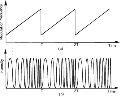
For coherent FMCW the maximum range which can be measured is limited by the coherence length, and to compensate for environmental fluctuations additional components are required (Jackson et al, 1982). Alternatively, an incoherent approach based o n intensity modulated F M C W w o u l d be an attractive possibility since coherent light is not required. In this approach a subcarrier is modulated instead of the optical carrier. Incoherent F M C W m a y alleviate s o m e of the noise sources encountered in the coherent F M C W system while significantly reducing the overall system complexity. By modulating a laser diode's drive current, the intensity of the emitted light is varied (section 5.2). Hence, to achieve an J F M C W output, the modulation frequency of the drive current is chirped (Collins, 1991). The required modulation behaviour is s h o w n in Fig 3.4.
Since only intensity variations are of interest, a multimode laser diode can be used, giving the added advantage of greater power, which is desirable for long
Time
Time
Fig 3.4 Modulation behaviour: (a) modulation frequency and (b) intensity
The modulation frequencies used in incoherent FMCW are normally within the JRF range to ensure that the resolution is reasonable. If these are extended into the microwave region, specialised electronics are required. In either case the sweep frequency is at least 2 orders of magnitude smaller than those obtained in coherent F M C W . According to Eqn. 3.4, the wider the sweep frequency range, the better the range resolution. Thus the possible resolution for incoherent F M C W will be less than for the coherent case. However, since incoherent F M C W can measure a wider range, the fractional resolution should be similar in both instances.
constant-amplitude R F signal with a periodic linear sweep frequency. T h e detected optical reflections were delayed by propagation through the fibre to produce a difference in the modulation frequency. This w a s mixed with the local source drive signal to produce a beat waveform, which w a s observed o n a spectrum analyser. The frequency axis of the spectrum w a s proportional to distance along the fibre, and very w e a k reflections in optical fibres were measured. With this experimental system it w a s possible to detect end reflections from a 2.2 k m length of fibre w h o s e far end w a s immersed in index-matching fluid to eliminate the Fresnel reflection.
Recently the Boeing Aircraft Corporation (Abbas et al, 1990, de la Chapelle et al, 1991 and Vertatschitsch et al, 1991) investigated a high-precision laser radar based o n this incoherent F M C W technique for possible use in aircraft monitoring and control systems. The basic arrangement of this chirped intensity modulated laser radar is depicted in Fig 3.5.
Laser
diode 15 m 15 m Fixed Target
,«—v reference R2 R3
At/
\<0-Fibre tip Connectors R4 Photodiode
Signal processor
Corner cube
R5
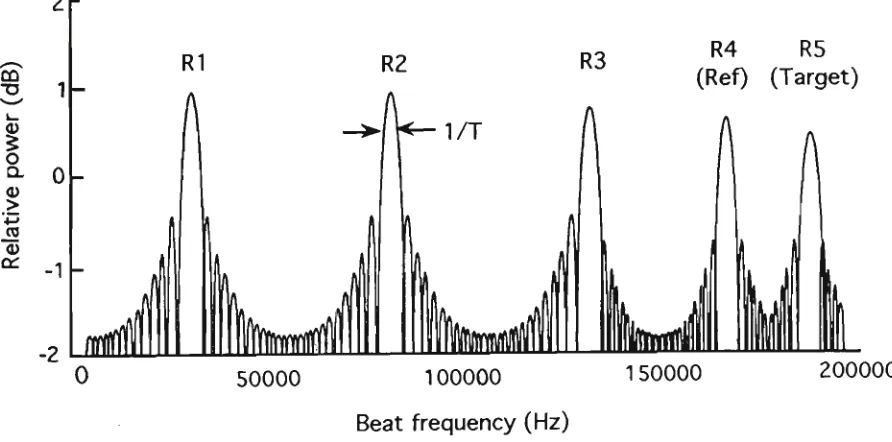
Fig 3.5 Basic principle of the chirped-intensity modulated laser radar (after Abbas et al, 1990)
The reflections from the target and the fibre tip were both 4%. The output from the photodiode w a s mixed with the signal from the R F chirped source to
produce several beat frequencies. Fourier processing w a s used to estimate the beat frequencies of the target and the reference end whilst minimising the effects of the extraneous signals produced by the unwanted connector reflections. By use of the reference reflection, environmentally induced variations in the fibre propagation length were subtracted from the target range. A typical beat spectrum is s h o w n in Figure 3.6.
The cliirp frequency used was in the microwave region (2 GHz to 8 GHz), with a target range of u p to 120 m m and 0.1 m m resolution. H o w e v e r , the electronics required were complex and therefore expensive.
R4 R5 (Ref) (Target)
50000 100000 150000 200000 Beat frequency (Hz)
Fig 3.6 Beat frequency spectrum (after de la Chapelle et al, 1991)
3.5 Summary
As discussed in this chapter, range measurements based on laser diodes (or lasers) and optical fibres have several advantages over other measurement methods (sections 3.2, 3.3), including high collimation, high resolution and low weight. A m o n g s t the methods using laser diodes, the time of flight method is straightforward in principle but needs complex electronic processing for high resolution (section 3.4.1). The phase shift measurement needs m o r e than one intensity modulation frequency to overcome possible ambiguous range problems (section 3.4.2). The coherent F M C W method has excellent resolution but the measurement range is limited by the coherence length of the source (section 3.4.3). Expensive single-mode laser diodes are required w h e n large ranges are to be determined (section 2.2.1), and additional stabilising components are necessary.
Chapter 4 Theoretical analysis
4.1 Introduction
Applications of FMCW techniques were discussed in Chapter 3 and its principle w a s described briefly. A detailed examination of F M C W is presented in this chapter including Fourier analysis, from which the beat frequency m a y be inferred (section 4.2). This is based o n the treatment given b y H y m a n s and Lait (1960). The signal to noise ratio (SNR) of the whole system is also calculated and compared with that measured (section 4.3).
4.2 Fourier analysis of FMCW ranging
4.2.1 The beat waveform expression
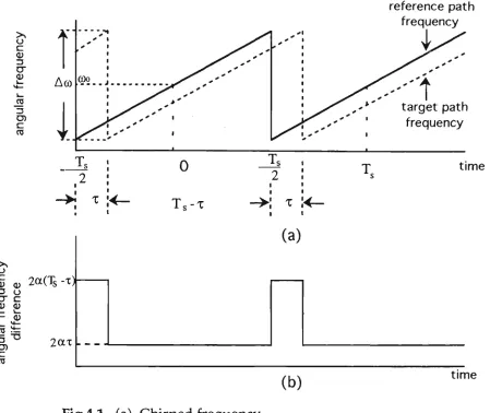
In an FMCW system, the modulated source produces a signal whose frequency
is varied in a sawtooth fashion (Fig 4.1(a)). The solid line is the instantaneous frequency from the reference path, while the dotted line is the instantaneous frequency due to the reflection from the target (Fig 4.1(a)). The returned signal from the target has a time delay T compared with the reference path. The r a m p period is Ts and the angular frequency sweep is AGO. For convenience, the sweep
rate is taken as 2 a (2a = — , Aco = 2nAf where Af is the frequency sweep as
T
s
>>
o c
3
tT
CD
.ro
O)
c
ro
g <„ 2a(T
s-T)-2. °
cr c
2. 2
c
ro
(b)
reference path frequency
time
time
Fig 4.1 (a) Chirped frequency
(b) Instantaneous frequency difference of the two paths
The instantaneous angular frequency coj is given by the following expressions: 0)i = a>o + 2at
= coo + 2a(t-T
s)
where - ^ T
s< t < ^Ts
where -\T
S<t< JT
S(4.1) = coo + 2a(t - n Ts)
where Ts is the sweep period.
where ,k2n-l)Ts < t < ±(2n+l)Ts
M a k i n g the substitution:
tn = t - n Ts (4.2)
o)i = coo+2atn where - ^ Ts< tn< ± Ts (4.3)
N o w the phase <l>i at time t is obtained by integration of coi, n a m e l y
§i = I (Oidt + constant (4.4)
B y substituting Eqn. 4.3 into Eqn. 4.4, the general expression for the phase (fa) is found to be
<l>i = «otn + atn 2
+ no)oTs (4.5)
4.2.2 Production of the beat note
At the receiver, the reference path produces a signal Vgsin <j>g whilst the target path signal is Vesin())e, where (J>e is delayed in time by % compared to <J)g and
from section 3.4.3, _ measured range _ 2R
velocity of propagation c
and Vg, Ve are the amplitudes of the reference signal and the detected signal.
In a non-linear device (section 5.8.3), these two signals will beat together, and the resulting signal will contain a product term GVeVg sin<J>e sin<|)g, where G is a constant determined by the non-linear device used (section 5.8.3). Using
trigonometrical identities, then
VgVe sin tye sin <])g = J-VgVe[cos((|)g - <|>e) - cos((|)g + $e)]
im*
The phase-sum term, i-VeVgCOs((|)g+(j)e), is an oscillation at carrier frequencies
JJW
^VeVgcos(<|)g-(|)e) contains all the range information of interest. This term shall n o w be investigated.
From Fig 4.1(b), it can be seen that two separate cases of the receiver signal arise. These are as follows :
During the time interval - —Ts <tn< -J-Ts + i
<l>e = coo(tn-i -x) + a(tn.! - T) 2
+ (n-l)cooTs
<t>g = G>otn + atn 2
+ ncooTs
So <t>g-<t>e = o)ox - a(Ts-x)2 + 2a(x -Ts)tn (4.6)
Also during the time interval _ Ljs + T < tn < —Ts
2 * 2
<t>e = ©o(tn - x) + a(tn - T) 2
+ ncooTs <))g = cootn + atn
2
+ nco0Ts
So (|)g - (l>e = cooi - ax2 + 2axtn (4.7)
4.2.3 Frequency analysis of the beat signal
Using Fourier transform techniques (Champeney, 1985), the beat signal can be resolved into its separate harmonic c o m p o n e n t s . In general, the Fourier transform of the signal f(t) m a y be evaluated b y
F(oo) = f(t)e-j«tdt
Thus, for the difference term yVeVgCOs((|)g-(|)e), its Fourier transform is
•0
F(o)) = ^V
eVgcos((t)g-(t)e)e1
G)t
cit
By substituting t = t
n+ n T
s(Eqn. 4.2) and using Eqn. 4.6, Eqn. 4.7, then
j..LTs+x
F(co) = l v
eV g [ X e-JncoT
s][ cos[Q)oX-a(T
s-x)
2+2a(x-T
s)t
n]e-Jo)t
ndt
nn=-oo J-iTc 2l S
cos (o)ox-ax
2+2axt
n)e-j®t
ndt
n]
i-i-T
s+x
2
Note that the two integrals in the second bracket are independent of n and so
have been put outside the summation.
oo
The term £ e-JncoT
s= G)
S8(G>-kcos), where k = 0, ±1, ±2 ... and co
s=
2TC/TS.n=-oo
After integration, the Fourier transform of the beat signal (taking the allowed
values of k into account) can be usefully expressed as:
F(co) = l v
eV
gco
sX [8(<»-k(Ds)]
xt
Fl(
k(0s) +
F2(ko>s) + F
3(kco
s) + F4(kcos)] (4.8)
2
k=-~
Here
sin[(o>2ax)(^)] ,
F K © ) = (T
s-x) - r
2
— { d ^ - ^ 1 (4-9)
2[(co-2ax)(^)]
sin[(co+2ax)(^)]
v x^
F
2(co) = (T
s-x) - 2 — [ e ^
+sin{[©-2a(Ts-T)]J}
F3(co) = x 2_{e-j[cw-i<rs-T)]} (4 n )
2{[co-2a(Ts-x)]|}
sin{[co+2a(Ts-x)] x
-}
F4(co) = x ^ j j K w+i < rs- x ) ] j (4 1 2 )
2{[co+2a(Ts-x)]J}
4.2.4 Examination of the spectrum
The delta function in Eqn. 4.8 (S(co-kcos)) implies that the spectrum has the
form of discrete lines lying at integer multiplies of the ramp frequency cos.
From Eqn. 4.9 - 4.12, it can be seen that:
Fi(co) = F2*(-co) F2(co) = Fi*(-co) F3(co) = F4*(-co) F4(co) = F3*(-co)
where the "*" represents the complex conjugate. Since only co > 0 is of interest, Eqn. 4.8 can be rewritten as
oo
F(co) = lveVg cosX [S(co-kcos)] x [Fi(kcos) + F2(kcos) + F3(kcos) + F4(kcos) 1
k=0
+ Fi(-kcos) + F2(-kcos) + F3(-kcos) + F4(-kcos)]
or
oo
F(co) = ^VeVg cos X [5(®-kcos)] x [Fi(kcos) + F2(kcos) + F3(kcos) + F4(kcos)
+ Fi*(kcos) + F2*(kcos) + F3*(kcos) + F4*(kcos)]
2
F ( c o ) = l veVg c o s X [5(co-kcos)]x{2Re[Fi(kcos)l + 2Re[F2(kcos)]
k=0
2Re[F3(kcOs)l +2Re[F4(kcos)]}
T h u s the full analytical f o r m of the Fourier transform is as follows,
00
f F(co)= l v e V g X [o(co-kcos)] x { (Ts-x)
z
*=0
sin[(kcos-2ax)(%^)]
[(kC0s-2ax)(^l)]
2 COS(«>crr - iko^x)
sin[(kcos+2ax)(5^)]
+ (Ts-x) —-^—cos(o)oT+Lkcost)
[(kcos+2ax)(3|l)]
2
sin{rkcos-2a(Ts-x)] x
-}
+ x — cost^o* - ikcOsCrt-x)] {[kcos-2a(Ts-x)]|}
2
sin{[kC0s+2a(Ts-x)]^}
+ X — COS[o)oX {[kcos+2a(Ts-x)]|}
+ i-kC0s(T.-x)]} (4.13)
T h e details of this expression will n o w b e discussed. There are terms of the form —x_x (i
e
- sinc(x-Xo)) in Eqn. 4.13 which are shown generally in Fig 4.2. The maximum for this function occurs when x = XQ.
sinc(x-xo)
(x-xo)
Equations 4.9 to 4.12 indicate that only the sine envelopes for Equations 4.9 and 4.11 have m a x i m a occurring for co > 0. These occur when:
for Eqn. 4.9 coBi = 2ax
for Eqn. 4.11 coB2 = 2a(Ts-x)
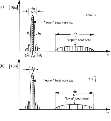
Normally x is very small compared to Ts since the measured range is not
particularly large. Thus it is appropriate to call C0Bi=2ax the "lower" beat note and coB2=2a(Ts-x) is referred to as the "upper" beat note. The time delay x = ^ ,
where R is the range to be measured, so the "lower" beat note (coBi=2ax) is proportional to R (in agreement with the simplified analysis given in section 3.4.3). Therefore b y measuring COBI, R can be determined. In typical F M C W applications where x « Ts, the "upper" beat note coB2 = 2a(Ts-x) « 2 a Ts = 27tAf
lies in the R F range and can be readily eliminated by a low pass filter.
Now it remains for the width of the sine envelope to be considered. From Eqn. 4.9, it has zeros w h e n
(co - 2ax)(^) = ± mix m = l,2,...oo
so the "lower" beat spectral width (ACOBI) is given by
AC0B1 =;F— (4.14)
1S-X
For Eqn. 4.11, zeros occur w h e n
[co-2a(Ts-x)] ^ = ± iron m = l,2,...°o
so in this case, the "upper" beat spectral width (ACOB2) is given by
An
A s already stated, the spectrum is composed of a series of discrete lines which are spaced in cos (the chirp frequency). These discrete lines are modulated by the
^ ) ] andsinc{[co-2a(Ts-x)] T
-functions sinc[(co-2ax)(^)j andsinc{[co-2a(Ts-x)]
T
-}. The actual beat frequency
(COBI) lies at the centre of the sine envelop (sinc[(co-2ax)(T^)J) and so is not necessarily equal to a harmonic of cos- That is, the beat frequency is not
normally expected to be one of the discrete lines of the spectrum.
The spectrum of F(co) is given in Fig 4.3, and it should be noted from Eqn. 4.9 and Eqn. 4.11 that
Amplitude of lower beat-note T -X
Amplitude of upper beat-note x
From this Fourier analysis, it can be seen that the spectrum of the beat waveform consists of two regions which are composed of discrete lines spaced by cos- If x is small the spectrum is expected to have the form s h o w n in Fig
T
4.3(a). O n the other hand, if x > -*•, the "upper" beat frequency will be smaller than the "lower" beat frequency and the spectrum will appear as s h o w n in Fig 4.3(b). Thus the unambiguous range of the F M C W method is *& - _x which
T c
means that the m a x i m u m measurement range is Rm ax = -T~- In this work, Ts =
( a ) | F(co)j
lower" beat note co*
small x
4*
upper" beat note
(b) | F(co)|
Zn$ 2nf Znf*
upper" beat note coB
4K
Ts-x
"lower" beat note
I
UfTrri 11111 rm>J
CO
CO
A series of discrete lines spaced in cos The beat frequency
Fig 4.3 Spectrum of beat note of
4,TC 47C\
(a) small x (Spectrum width of "lower" beat = - — < — )
J.s-X X
(b) x > !§- (Spectrum width of "lower" beat = -_^- > —)
4.2.5 Determination of the beat frequency
As described previously (section 4.2.4), the Fourier spectrum of the beat
waveform consists of discrete lines spaced by 22L and the beat frequency is not
ts
normally one of the discrete lines. In order to determine the beat frequency, it is necessary to fit these discrete lines into a sine envelope to locate the position of the central maximum. However, because of noise and VCO non-linearities
(section 5.5), this method is impractical. .Alternatively, for a short range, x « Ts,
then for the lower beat note envelope sine [(co-2ax)&-^)] = sine [(co-2ax)(^-)]. Also from Eqn. 4.14, ACOBI = ^— »•=- = 2cos, which means only two discrete lines
t s"X 1 s
lie in the central region of the sine envelope. If they have the values 27ifi and 2vrf2 respectively (F(27rf1)=hi, F(27uf2)=h2), and the beat angular frequency is 27cf
(2rcf = 2ax) (Fig 4.3(a)), then as described in section 4.2.4, sin[(2icf1-2irf)(^)]
^ — = bh! (4.15) (27tfr27lf)(^)
sin[(27if2-27cf)(^)]
and - ^ — = b h2 (4.16)
(2nf2-2nf)(f)
where b is a constant arising from other terms in F(co) (Eqn. 4.13).
Note that 27tf2 = 2n(\ + 22L (section 4.2.4), and by dividing Eqn. 4.15 by Eqn. 4.16,
Is
the beat frequency (f) can be obtained as
f _ hjfi +h2f2 (4.17)
h i + h2
Thus by measuring the amplitudes (hi and h2) of the two observed discrete
frequencies (fi and f2) in the central region, the beat frequency can be
4.3 N o i s e in electrical circuits
For any detection system, signal-to-noise ratio is an important parameter to consider in terms of signal quality. The major sources of noise are thermal noise (or Johnson noise) and shot noise (Palais, 1984).
4.3.1 Thermal noise
Thermal noise originates in a photodetector's load resistor. Thermal noise power ( W ) is calculated from
PTN = 4kTAfRL
Where PTN = thermal noise power k = Boltzmann's constant T = temperature (K)
Ai = receiver's electrical bandwidth (Hz)
R L = resistance of load resistor (Q)
Note that the thermal noise spectrum has essentially a uniform frequency distribution (Palais, 1984).
4.3.2 Shot noise
In semiconductor photodetectors, shot noise arises from the random
generation and recombination of free electrons and holes. T h e shot noise power ( W ) is
PS N = 2e(is + lD)AfRL
is = the average detector current (A)
I D = photodetector's dark current (A)
The shot noise spectrum is also generally uniform over all frequencies (Palais, 1984).
From these expressions, it can be seen that both thermal and shot noise power are proportional to the detector's bandwidth. Thus a bandpass filter (which reduces the bandwidth to the range of interest) (section 5.8.1) will usefully1 decrease the noise level.
4.3.3 Signal-to-noise ratio (SNR)
For a photodetector, having an incident optical power P(W) and responsivity p (A/W), its photocurrent is given by
Is = pP
Thus the average electrical signal power is
PES = IS 2
RL=(PP)2RL
Therefore the SNR of the detector is
SNR = P
ES = (PP)2RL (4.18)
P T N + P S N 4kTAlRL + 2e(pP+ID)AfRL
For the PIN photodiode selected (section 5.3), using typical values of P = 0-4 A / W , R L = 50 Q , T = 293 K, I D = 0.02 n A (which can be omitted in the calculation
since ID « is), Af (before bandpass filter) = 400 M H z (which is the selected
SNR =
(0.4xl2.6xl0"6)2x50
(4xl.381xl0-23x293+2xl.602xl019x0.4xl2.6xl0-6)x400xl06x50
=>SNR= 3.92
If expressed in dB, then the SNR becomes 10 logioSNR = 5.9 dB
The measured signal and noise power is given in Fig 4.4 which was obtained from an Advantest TR4131 Spectrum jAmalyser. The resolution bandwidth of
this spectrum analyser was 10 IcHz, and the average signal power was -26.2 dBm. From 0 to 280 M H z , the average noise power was -77 d B m (20 p W ) and from 280 M H z to 400 M H z (the selected bandwidth of the oscilloscope), the noise power was -73 d B m (50 pW). Thus the total noise power was
irti r ™ ^ Q 280xl0 6
eft ~ (400 - 280)xl0 6
1
lOlogio! 20xl0"9x +50xl0"9x- ]
10xl03 10xl03
= -29.4 d B m
Therefore the measured S N R was -26.2 d B m - (-29.4 dBm) = 3.2 dB
This SNR is too low to obtain a good quality signal, but since the chirp frequency for the Type 9036 V C O (section 5.5) was from 226 M H z to 271 M H z , a
A n Avantek VTO-9032 V C O (section 5.5) w a s also used to chirp the laser diode's modulation frequency over the range 300 M H z to 680 M H z . A 1 G H z bandwidth w a s chosen w h e n using the oscilloscope. A second bandpass filter corresponding to this frequency range was required (section 5.8.1) whose 3 dB bandwidth w a s from 200 M H z to 700 M H z . According to Eqn. 4.18, the S N R should n o w be 4.96 d B and the measured S N R is given in Fig 4.6 which shows an average signal power of -26.2 d B m . The noise power, from 200 M H z to 700 M H z w a s -74 d B m (40 p W ) , whilst elsewhere it w a s -87.5 d B m (1.8 p W ) . Thus the total noise power was -27 d B m , and so the measured S N R was only 0.8 dB.
4.3.4 Summary
From the calculations and the measurements above, it can be seen that the S N R is insufficient to obtain a good quality signal even w h e n a bandpass filter is used. The signals on the oscilloscope from the photodetector and the bandpass filter are given in Fig 5.22(a) and Fig 5.22(b) respectively and can be seen to have poor S N R . To overcome this an electrical signal processor w a s developed, and this is described in section 5.8.3. W h e n processed in this way, a beat frequency was produced, and by appropriate filtering, the S N R was greatly improved (section 5.8).
(a)
495MHz
T
1GHz
ota/
10ms/
3
3
i
• i
<
X
1
I
1
J
1 1
-1 1 ~i
'
I
ATT iOdS
(b)
-20dBjTi
AV
500MHz
1GH2
j i0<p8/
•faOWHzW
^ k * ¥ * M W «:^ ^
_1 !..._ i_. ._.J J L
ST 2 s /
ATT iOoS
1 i 1 1 _i j_ _
ST IOJTJS/ ATT 10d3
(b)
-20dBm 505MHz 1GHz
ST 2s/ ATT 10d3
(a)
OdBm
502MHz
.GHz
10^18/
dook^zw
ST iOms/
ATT iOdB
(b)
-20dBm
1
1502MHz
J
1 i.„
.
1 -* '
i *>
-; ; i
< * i
j ! ;
!
• • i — • j
• * i : j ] 3 1 : i i • * -* • i i 1
~T .,_..
1GH:
! IOdB/
< ivMi/W^ST 2s/
i^V<Wf«J*HM J.ATT IOdB
_.»._Chapter 5 Experimental details
5.1 Introduction
VCO
JMV
Laser diode
Function generator
Oscilloscope
I
Signal processor
Bandpass filter
Reference fibre (50/125 \im)
fUST)
:rlector Electrical cable Optical fibre
Collimator
Reflector
A R coated Variable air path fibre end
Fig 5.1 Experimental arrangement
5.2 Laser diode source
5.2.1 Laser diode source and modulation circuit
HHi'
HH'
.3
V L ^ H I - S
HH
HH
1
-j owsi
"|-m cn SO r-J O
5
o8 8
HH' H H
-*-| nzz "| t | uosi |
r-L3!lZr—i
uot.a "8
of"
4
-4-H"
«.§
CUI Cs| o
! S3
W ' mf^. ^
¥
Cfl-| ozz [•
H ooot
1-N
O 89
-Hi'
.J-3 fl]
° &
a
3.3G & S o
m W , which implies a modulation depth of 100%. The m a x i m u m modulation power allowed for the laser diode w a s 0 d B m . However, since this circuit lacks a temperature control system, the D C output power, modulation depth and output m o d e might vary. Since only the beat frequency formed by the chirped intensity modulation is of interest, any temperature change is not expected to have a significant effect o n the final result. This circuit is effective for modulation frequencies from ~10 M H z to 1 G H z and has an input impedance of 50 Q. A lens w a s bonded at the focal point of the laser diode radiation area in order to enhance the coupling of light from the laser diode to the butted optical fibre. The continuous working output power coupled into a 50/125 p.m graded index multimode fibre w a s -2.4 d B m .
5.2.2 Modulation optimisation for the laser diode circuit
The depth of optical modulation (section 5.2.1) is an important factor affecting signal quality (Oppenheim et al, 1983), and for an analogue drive current for an
L D , the m a x i m u m modulation is s h o w n in Fig 5.3 (note for analogue modulation, the D C current is set to Ibias)- The best S N R should occur w h e n the modulation depth is as high as possible, and this happens w h e n the peak-to-peak modulation current is double Ibias (Fig 5.3), which is difficult to achieve in practice.
Time
Drive cuirent(A)
Time
Fig 5.3 M a x i m u m analogue modulation for a laser diode
Modulation
circuit LDA
4 2JMHZ
Signal generator
9V
B P W 3 4
photodiode 0.1 nF
lkQ 10 kQ
II
OscilloscopeFig 5.4 Arrangement used to measure the depth of modulation of the L D
The depth of modulation can be optimised by changing the emitter impedance (Ze) of the A T 0 1 6 3 5 transistor (Fig 5.2) (Horowitz and Hill, 1989), although any
change will also affect the frequency response of the circuit. T o optimise the depth of modulation while maintaining a relatively flat frequency response (Fig 4.4(a)), several trials with different Ze were conducted before a suitable
Although the modulation depth was measured at 2 MHz, rather than at the modulation frequencies employed in this experiment, this should still be a
reliable estimate of the actual depth of modulation. The figure obtained, of 63% is a reasonable value to work with.
58raV
yaia
trlsfd
1
-3. ?25n V—: : : : : = = • =
>258ns leans/dlw E Q 742ns
Fig 5.5 Intensity modulation of the laser diode output
5.3 Photodetector circuit
A silicon PIN photodiode (008 UDT) was selected because of its good
responsivity, low dark current and large bandwidth (section 2.2.3). Its typical responsivity at 780 nm is 0.4 A/W, and its response time of 0.35 ns is fast enough to detect signals up to several hundred megahertz. The dark current is 0.02 nA. The photodetector's transconductance amplifier circuit is shown in Fig 5.6 (Shelamoff, 1992). Two wide bandwidth amplifiers were used, namely an
/?H"
PUa
MHr
^ ESI
5 <
5 co%mt tu Q. r-• * * «,
m 00
55 *^ « ,—* > < < H 4-1
3
o u •7-{ b O 4-" uand a bandwidth of 750 M H z , and an Avantek MSA-0685 integrated amplifier whose gain is 18.5 d B around 500 M H z with a bandwidth of 800 M H z . Thus the total gain of this amplifying circuit is 91 dB, but to ensure a linear response, the m a x i m u m optical power into the photodetector w a s limited to -9 d B m .
5.4 Frequency response of the combined source and detector system
The arrangement used to measure the system's frequency response is shown in Fig 5.7. Since the m a x i m u m optical input power allowed by the detector is -9 d B m (section 5.3), and the power from the laser diode is -2.4 d B m (section 5.2.1), a variable optical attenuator w a s required. A n Advantest TR4153A tracking generator with 0 d B m output w a s employed to modulate the laser diode, and the detector circuit output was displayed on an Advantest TR4131 R F spectrum analyser. This R F spectrum analyser has a wide adjustable bandwidth from 100 k H z to 4 G H z .
tracking generator
1
laser source
V
spectrum anal yser
dp.ter.tnr
| optical | I attenuator 1
r
— optical fibre — coaxial cableFig 5.7 Measurement of the system's frequency response
spectral response is illustrated in Fig 4.4(a), which shows that the system 3 d B bandwidth covered the band 75 to 975 M H z . This figure w a s compatible with
the modulation frequencies obtained from the V C O s (section 5.5), namely 226 to 271 M H z and 300 to 680 M H z .
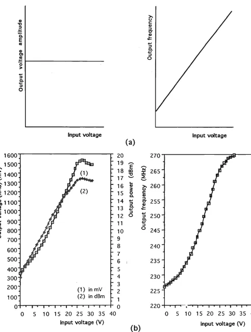
5.5 Voltage-controlled oscillators (VCOs)
« •o 3 O. E a o O) a mm. o > 3
a
£ 1000
^
900%
800°
700Input voltage
i • i « i • i
15 20 25 30 35
Input voltage (V)
(a)
E CQ 13 0)I
a
*-> 3 CL Input voltage N DC 2 270 265 260" v 3 IT 0) 255 3 o 250" 245" 240 235" 230 225" 220(b)
Input voltage (V)1000
i
<>> 2 oc **^ 0) cn n JjW o > tmi 3 O 4-< 3o
900 800 700 600 500 400 300 200 1000
-I
(1) inmV -2 (2) in dBm •
0
• i i i i i i i i i i i i
2 4 6 8
10 12 14 16 18 20Input voltage (V)
. • • • • i i i i i • .
8 10 12 14 16 18 20 Input voltage (V)
Fig 5.9 Output characteristics of the VTO-9032 V C O
5.5.1 Attenuators for the V C O output
The m a x i m u m input modulation power allowed for the laser source (section
5.2.1) w a s specified as 0 d B m , whilst the m a x i m u m output power from the
Type 9036 V C O was, in fact, 17 d B m (Fig 5.8(b)). Therefore a 17 d B attenuator
with 50 .Q input and output impedance, shown in Fig 5.10, was constructed.
W h e n the Type 9036 VCO's output w a s connected through this attenuator, the
suitable characteristics s h o w n in Fig 5.11 were obtained. The output voltage
amplitude is thus reduced to the required amount, whilst the frequency
C-
39 nI
I
Fig 5.10 17 d B attenuator
The characteristics for the Avantek VTO-9032 VCO (Fig 5.9) show that its m a x i m u m output p o w e r is 13 d B m , so a commercial 13 d B attenuator w a s acquired. W h e n using this attenuator in conjunction with this V C O , the output static characteristics s h o w n in Fig 5.12 were obtained, and indicate that the overall output voltage amplitude has been suitably reduced without affecting the frequency response.
2 4 0 .
12201
S200:
2 £180. 0) 2>160-co *->1\ 140.
3 120. CL
gioo.
80"_60 J
40; 20^ 0 jgpl J*L" 1 1 1 —
0 5 10 15
/ ( I )
/y (2)
(1) in d B m (2) i n m V
— 1 1 1 r
20 25 30 3
Input voltage (V)
0 " -1 " -2 " -3 " -4 " -5 ' -6 -7 ' "8 ~ -9 ; -10
' -n
I5 E CQ T3 Sw-L. 0 *-> 3 a.*-> 3 O 1 N X 2 0 V 3 cr <u ^ *-i 3 Q. 3 O 270 265 260 255 250 245 240 235 230 225 220
0 5 10 15 20 25 30 35 Input voltage (V)
240
>
2 2
°"
(RMS ) ( m 0 3 O
o
o
§,160" ca 15 140" 3 120"3-O 100" 80" 60" 40" 20" 0 -JEHiL
Air
// (2)
|U &
>
• 1 1 1 1 1 1 1 1 1
H
\ L "JVra
(1) inmV (2) in d B m
• i • i i i • i •
• 2
" 1 E
CO
:° r
m)
" " I l
a. c o r o Outpu t - -4 ~ -5
!" "6
" -7
" "8 !" "9
-10
0 2 4 6 8 10 12 14 16 18 20 Input voltage (V)
Fig 5.12 Output characteristics of VTO-9032 V C O plus 13 d B attenuator
5.6 Optical fibres and directional coupler
5.6.1 Optical fibres
50/125 um graded index multimode optical fibre (section 2.2.2) was used throughout these experiments. T w o pigtails were used to connect the laser diode to the coupler and the coupler to the photodetector. A length of around 25 metres of fibre w a s used for the reference path. T w o G T E Fastomeric mechanical splices (Fibre Optic Products) and a n u m b e r of fusion splices were used for necessary connections (section 2.3). T h e typical losses through the mechanical splice and fusion splice were about 0.5 d B and 0.1 dB, respectively.
700
300 i • i • i • i ' i • i • i • i • i •
2 4 6 8 10 12 14 16 18 20
5.6.2 Directional coupler
A 2x2 fused biconically-tapered directional coupler (Fig 5.13) w a s selected to split the light from the laser source into the two required paths (Palais, 1984). It w a s designed to provide low loss coupling with a range of splitting ratios. The splitting ratio of the coupler is 50:50 at a central operating wavelength of 850 n m . T h e characteristics of this coupler operating at 780 n m were obtained by using the arrangement given in Fig 5.14. It w a s found that the p o w e r distribution between the paths w a s equal, with s o m e loss in the coupler. A s s u m i n g the loss in the mechanical splice w a s 0.5 d B and the loss in the fusion splice w a s 0.1 dB, then the excess loss of the coupler w a s 0.5 dB.
Fig 5.13 Fused biconically-tapered directional coupler
Laser diode
. Mechanical
1
f
1
splice -2 4 d B m
output
_
50:50 coupler
Fusion "6 5 d B m splice
/ * bare fibre
adaptor N
\ \ Fusion
splice _6-5 dj
Power meter
Power meter
im
5.7 O t h e r optical c o m p o n e n t s
5.7.1 Collimators
Two lenses were selected for collimating the light launched into the air from the optical fibre end. A single microscope objective with magnification of x20 and a 4 m m focal length w a s used initially. H o w e v e r as a microscope objective is designed -for short distance collimation only, it did not perform well over long distances (~5 m ) . A 1 m focal length thin lens w a s used in addition to the microscope objective in order to improve the collimation, but even then the results were still far from ideal (section 6.3).
As a different approach, an 8 cm focal length concave mirror was used as a collimator, with the optical fibre end located at its focus. The collimated light spot w a s larger than that obtained with the lenses but, m o r e importantly, provided greatly improved collimation (section 6.3).
5.7.2 Reflectors
Three types of reflectors were used in this work. The first was a thin film (Tj02) reflector which w a s deposited onto one end of a fibre using v a c u u m coating
( E d m u n d Scientific Co., 1989). Since a mirror will only d o this at normal incidence, corner cubes are ideal w h e n precision alignment is difficult or time-consuming. There are three total internal reflections within the corner cube (Smith, 1970) as s h o w n in Fig 5.15.
Fig 5.15 Corner cube reflection
5.8 Electrical processing of detector output
The output of the basic experimental arrangement shown in Fig 5.1 was an RF carrier being modulated at the beat frequency (section 3.5 and Fig 6.9). A variety of circuits were built in an attempt to demodulate the output and obtain a more useful signal from the sensor. Whenever circuits involving high frequencies were required, special care w a s taken to ensure that unwanted capacitive or inductive effects o n circuit boards were minimised (Bowick, 1991).
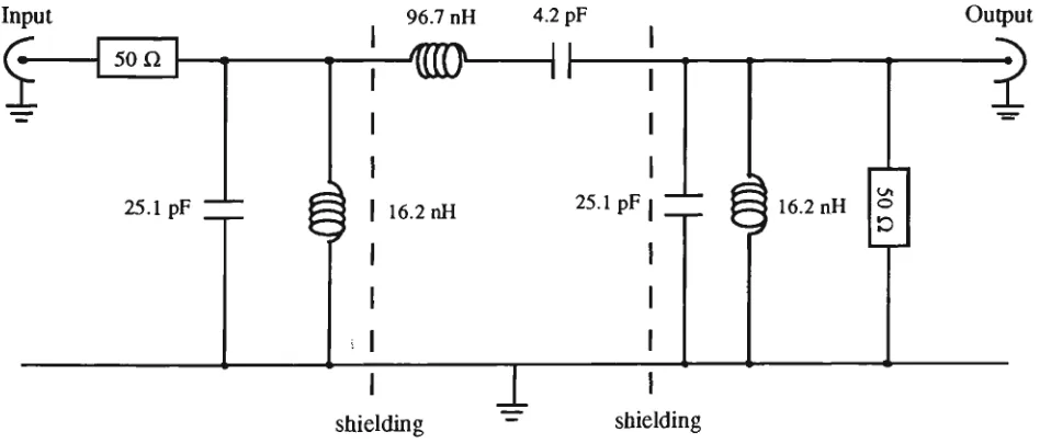
5.8.1 Bandpass filters
4.3.3), and is given in Fig 5.16. However, mutual inductance between components resulted in several unexpected resonances, and was reduced by placing two copper shielding plates between the components. With the filter included (Fig 5.17), the system's response spectrum was as shown in Fig 4.5(a). The resultant 3 d B bandwidth was from 170 M H z to 330 M H z , and the insertion loss w a s very small which can be seen by comparing the m a x i m u m response shown in Fig 4.4(a) and Fig 4.5(a).
For the Avantek VTO-9032 VCO, the sweep frequency range was 300 MHz to 680 M H z (section 5.5). Another bandpass filter was designed (Fig 5.18) (Bowick, 1991) for which the 3 d B bandwidth was from 200 M H z to 700 M H z , with a small insertion loss. The system's response spectrum, with the bandpass filter included, is s h o w n in Fig 4.6(a).
Input
f
501125.1 pF —""
96.7 nH
16.2 nH
4.2 pF
• W
II-25.1 pF
Output
16.2 nH
-2
T
shielding shielding
tracking generator
i
lasei source
C
v
spectrum
ana lyser
bandpass filter *
rjftfertnr
optical j attenuator J
r
— optical fibre
- coaxial cable
Fig 5.17 Measurement of the frequency response including the bandpass filter
Input 24.2 n H 4.2 pF
w—
16.2 n H 6.27 pF
T
: 16.2 nH
Output
2
shielding
Fig 5.18 Bandpass filter circuit (200 M H z - 700 M H z )
5.8.2 Pre-amplifier
photodetector w a s too small for a diode because of the usual cut-in voltage (Fortney, 1987). Therefore, a pre-amplifier circuit w a s designed (Fig 5.19), using a fast response Avantek M S A - 0 1 8 5 amplifier with 17.5 d B gain. T h u s a sufficiently large signal voltage (~ 200 m V peak-peak) w a s obtained for use by the non-linear circuit.
Input
22 pF Avantek MSA-0185
A +15 V
power supply
ON
1.
T
1000 pF
22 pF
Output
Fig 5.19 Pre-amplifier circuit
5.8.3 Electrical signal processor
CQ
>
< T C j
00 0=
01 BE
CD N PE
ro
s«
-K-o
s © — I I "
Oi Ol O N ? . . . pi <n ^- M ^ ..
31323233
oooo0*000000
.—• ,—i ,—i ,—, c n
•• O — «N
*L* L I ? S
H O J 2
j Z J o <n r-i u^ •* n
a ar ~ t^ 5 i n
D
.-•.-••^•g-oo<sc-i o o o o o o o o ©ooooooo
^-icsciTj-w-ivor-oo
u u u u a a u u
N
T h e role of the non-linear circuit can be understood as follows (Horowitz and Hill, 1989):
When the input voltage (from the pre-amplifier (section 5.8.2)) lies within the non-linear part of the diode's forward voltage-forward current curve, the
output current (I) will change with the input voltage (V) as below:
I = a + bV + cV2 + dV3 + ...
where a, b, c, d ...are constants determined by the curve shape. The input voltage V = Visincoit+ V 2 sino)2t (where Visincoit and V2Sino)2t are the voltages due to the reference and target paths, and coi and 0)2 are chirped and differ by a constant a m o u n t because of the path difference).
A simpler analysis than the Fourier analysis of the beat signal given in section 4.2 will be described here. Assuming cubic and higher order terms of I can be
neglected, the output current will be
I = a + b(Vi sincoit + V2 sinG)2t) + c(Vi sino)it + V2 sinco2t)2 = a + b(Vi sincoit + V 2 sin©2t) + c(Vi2 sin2coit +V22sin2o)2t
+ 2Vi sincoit x V2 sinci)2t)
Note that the terms V i2 sin2coit and V22sin2o)2t only have Fourier components at 2G)I and 2©2 respectively. The cross term m a y be rewritten as:
Vi sin coit x V2 sin a>2t
= Vi sin coit x V 2 sin (a>i + 2ax)t
= I V i V 2 [ COS (<D2 -fi>i)t - cos (002 +G>i)t ] 2